Designing of strongly confined short-wave Brillouin phonons in silicon waveguide periodic lattices
††journal: oe††articletype: Research ArticleWe propose a feasible waveguide design optimized for harnessing Stimulated Brillouin Scattering with long-lived phonons. The design consists of a fully suspended ridge waveguide surrounded by a 1D phononic crystal that mitigates losses to the substrate while providing the needed homogeneity for the build-up of the optomechanical interaction. The coupling factor of these structures was calculated to be for intramodal backward Brillouin scattering with its fundamental TE-like mode and for intramodal forward Brillouin scattering. The addition of the phononic crystal provides a attenuation of the mechanical displacement after only five unitary cells, possibly leading to a regime where the acoustic losses are only limited by fabrication. As a result, the total Brillouin gain, which is proportional to the product of the coupling and acoustic quality factors, is nominally equal to the idealized fully suspended waveguide.
1 Introduction
Stimulated Brillouin Scattering (SBS) is a non-linear phenomenon that arises from the coherent coupling between light and sound. Thermal noise driven acoustic waves scatters a strong pump wave to a red-shifted Stokes wave, mechanical vibrations in the medium are then further stimulated by the optical forces resulting from the beating between pump and scattered waves, creating thus a feedback-loop that can efficiently transfer energy from the pump to the Stokes wave [1]. Experimental studies of SBS began with optical fibers due to their long interaction length and relatively small optical mode areas [2, 3, 4]. With the advances in microfabrication, it was possible to bring SBS to the subwavelength-confinement scale, where enhanced effects of radiation pressure granted a higher power transfer between pump and probe, despite the small interaction lengths [5, 6, 7, 8]. Since its first experimental demonstration [9], not long after the first laser demonstration, SBS-based devices have been explored in many applications ranging from sensors [10, 11], notch filters [12, 13, 14], RF-signal processing [15, 16], enhanced gyroscope [17], lasers [18, 19, 20, 21, 22, 23], and as a platform for exquisite studies [24, 25, 26].
However, mechanical confinement still remain a challenge for achieving large Brillouin gain in CMOS compatible integrated waveguides. Due to the lower acoustic speed of silica when compared to material such as silicon or silicon nitride, the vibrations excited in the device layer is partially transmitted to the substrate at their interface [27, 28], as opposed to more exotic platforms like soft glasses in which acoustic waves are trapped by total internal reflection [29]. For monolithic platforms one popular solution to this problem is to partially [28] or completely undercut the substrate [30, 31] to suspend the waveguides and isolate them from the substrate . While suspension is very effective at suppressing mechanical losses, it either requires a critical control of the residual anchoring [28] – which might affect distinct mechanical modes in different proportions – or rely on periodic anchoring points that ease the fabrication process [31, 32, 30].In this latter approach, the structural integrity of the suspended section can easily come into conflict with the necessary optomechanical interaction build-up length. When the characteristic gain length is comparable to the acoustic decay length the optomechanical interaction needs to build-up several acoustic decay lengths before reaching its expected performance [33]. This, however, is particularly difficult for Backwards Brillouin Scattering where the larger group velocity leads to a larger acoustic decay length. Although this regime has not yet been reached in silicon devices, it could become a reality with the increase in both coupling factor () and mechanical quality factor (). Reported in silicon waveguides [28, 30, 31] are still bellow silicon’s material limit [34] and any scattering and two-level systems induced by microfabrication process as shown by low-temperature experiments [35, 36].
One effective approach to overcome these limitations imposed by anchoring points is to explore a phononic crystal cladding along the suspended membrane. The crystal cladding prevents the mechanical vibration from leaving the active region and leaking to the substrate. It also shields the mechanical mode from any perturbation from the necessary periodic anchoring, reconciling the structural integrity with homogeneity needed for long-range Brillouin interactions. Indeed, previous works effectively explored this principle in the particular case of forward Brillouin scattering, where the mechanical waves have a null acoustic wavevector, [37, 16, 38]. However, silicon-based waveguide structures favoring the regime of backward Brillouin scattering, which has been shown to enable important functionalities [11, 13, 15, 17, 24] and, ultra-low mechanical dissipation [34] remains largely unexplored.
In this work, we investigate backward Brillouin interaction in a CMOS compatible waveguide design comprised of a silicon rectangular waveguide on top of a suspended silicon membrane. We overcome the impact of using anchoring points by surrounding the Brillouin-active waveguide core with a 1-D phononic crystal cladding that supports a full phononic band-gap – both shear and longitudinal polarizations – for short-wavelength acoustic modes. We start by highlighting the differences between the mechanical modes behavior in Forward (FBS) and Backwards (BBS) Brillouin scattering. The design process is then deeply discussed showing the phononic crystal cladding optimization for FBS and BBS while discussing the advantages of such design strategy and its expected performance compared to other waveguide design.
2 Backward and Forward Scattering
Forward and Backwards Brillouin Scattering are defined by the relative propagation between the incident and scattered optical modes, and are the two possible configurations that satisfy the phase matching condition in a waveguide geometry. For simplicity we will consider in this work the case of intramodal scattering, where the interacting optical modes comes from the same dispersion branch. Considering the phase-matching condition, illustrated in Fig. 1 (a), we can safely assume that the mechanical modes interacting via FBS are at the cut-off frequency regardless of the incident optical wave-vector, while in the case of BBS their mechanical wave-vector is roughly twice the value of the optical mode, meaning that the dispersion relations of mechanical modes can be no longer ignored.
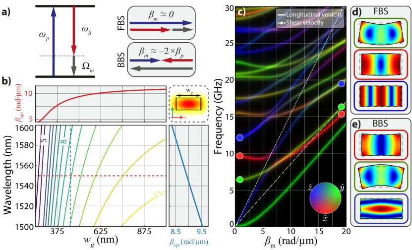
In order to gain some insight of the optical and mechanical modes involved in the BBS and FBS, we use finite element method (FEM) to simulate the optical and mechanical dispersion of a floating rectangular waveguide as shown in Fig. 1 (b)-(c). For a typical waveguide width and thickness used in CMOS compatible devices (waveguide width: ; silicon layer thickness: ), the optical wave-vector for the fundamental TE-like (inset Fig. 1 (b)) is in the telecom C-band. Two other important features arise from Fig. 1 (b). First, we notice that above the optical wave-vector is mildly affected by the waveguide width, since the rate in which the wave-vector changes with the waveguide width () has its maximum around (not show) and then monotonically decreases for larger waveguide width. This is an important feature when considering the geometrical dispersion in the BBS [39]. Second, by changing the pump frequency we can fine tune the optical wave-vector allowing for fine tuning of the BBS mechanical frequency.
Fig. 1 (c) shows the mechanical frequency dispersion for a waveguide width . Mechanical modes are colored according to the displacement ratio for each Cartesian direction, where red, green, and blue colors are related to , , and -dominant polarized modes; the polarization dependence is clearly seen for the mechanical modes shown in Fig. 1 (d).
Other than the phase matching condition, the Brillouin optomechanical gain over the scattered mode () – often called Stokes seed in pump-probe experiments – strongly depends on the transverse profile of both optical and mechanical modes by the expression:
| (1) |
where is the beating frequency between the pump signal and the stokes seed, is the mechanical quality factor, or Q-factor, is the effective linear mass density of the mechanical mode, is a Lorentzian function centered at and with full-width-half maximum (FWHM) given by the mechanical linewidth (), and () is the optomechanical overlap due to the photoelastic (moving boundaries) effect [6]. The coupling factor can be calculated by numerically computing the mode profile of both optical and mechanical modes using COMSOL Multiphysics ® FEM simulations. In the case of silicon waveguides however, we can already expect that -polarized (-polarized) mechanical modes should have larger gain for FBS [37] (BBS [40]); these modes can be readily identified using Fig. 1 (c).
As we depart from the cut-off region in the mechanical dispersion (), anti-crossing and hybridization become more common adding another layer of complexity to our problem. A relevant example would be the -polarized first order longitudinal mode (L(1)) [41, 42], highlighted in blue in Fig. 1 (e), which at hybridizes acquiring a Lamb-like character with significant displacement in the -direction.
3 Design
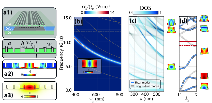
To mimic the previous floating waveguide, we propose a device that consists of a central rectangular waveguide on top of a suspended membrane that is mechanically isolated from the substrate by a 1-D phononic crystal cladding (PhnCC). Fig. 2 (a) shows a schematic of the design highlighting the main geometric parameters. We choose to fix both the central rib and the PhnCC at the same heights, so the whole mechanical structure can be fabricated in a single dry etching step. This is particularly important since multiple steps usually compromise the alignment between the nanostructures. We also opted to work around minimal support thickness since the Brillouin optomechanical gain would approach the one from the ideal floating silicon nanowire. So we considered for our simulations a Si thickness of and a etching depth of (), as well as other dimensions compatible with commercial foundries rules, which already proven to produce ultra-high optical and mechanical quality factor devices [43, 37].
3.1 FBS design
We separated the design process for this structure between the Brillouin Active Region (BAR), and the Phononic Crystal Cladding (PhnCC). We approximate the BAR to a fully suspended rectangular waveguide; this is a valid approximation since in a ridge waveguide most of the Brillouin optomechanical gain occurs in the central portion, which has a higher optical field density. This approximation makes the BAR design much simpler – as long as the waveguide support does not significantly affects the optical and mechanical modes, which is the case for .
In Fig. 2 we show the design process of a waveguide optimized to harness intramodal FBS using the fundamental TE-like mode. Similar discussion was thoroughly addressed for silicon bullseye-type cavity [37] and silicon nitride waveguides [38]. The Brillouin optomechanical interaction tends to increase for tighter confinement of both optical and mechanical modes, as shown by the coupling factor () map in Fig. 2 (b), however, excessive compactness has been reported to deteriorate the optical propagation losses [44]. In order to maintain a lower optical loss we kept in our design.
For the considered geometrical parameters mode that yields the highest intramodal FBS , is the L(2)-Mode (breathing-like) [41, 42] around . To confine this mode is necessary to tailor the phononic crystal’s parameters to create a bandgap that encompasses this frequency. Since this mode is planar at cut-off(, and ) [42], a partial bandgap considering only modes that are also planar is sufficient to confine it, this makes the waveguide design within our fabrication constrains relatively simple. In Fig. 2 (c) we show the evolution for the density of states (DOS) of the PhnC as a function of the lattice parameter (), where the filling factor () is kept constant. It is clear from this graph the relation between the mechanical bands frequency and , showing that we can easily find a bandgap of several GHz around the desired frequency just by tuning .
As the PhnCC is attached to the BAR, both the mechanical and optical modes of the BAR might hybridize with modes from the support slab. In the case of the optical mode the slot effect can be avoided by making the support width () larger than the mode penetration depth in the air region, which is roughly in our case. Due to the large -displacement at the edges, the -mode easily couples to the slab’s dilatational mode, like this mode can be understood as an acoustic Fabry-Perot mode and so the mechanical frequency decreases with the slab width ( in this case).For certain values of we expect to see crossing between the -polarized dilatational and the -polarized shear modes. Regions near these crossing points should be avoided in order to preserve the mechanical mode integrity.
Fig. 2 (d) shows the band-diagram for the final phononic crystal design together with the FBS frequency for the BAR structure (red solid lines) and the resulting FBS frequency for the waveguide structure depicted in Fig. 2 (a2) (red dashed lines). The frequency difference between the BAR and final structure is small when compared to the bandgap width, not affecting the final gain values significantly, thus supporting our design strategy for FBS.
3.2 BBS design
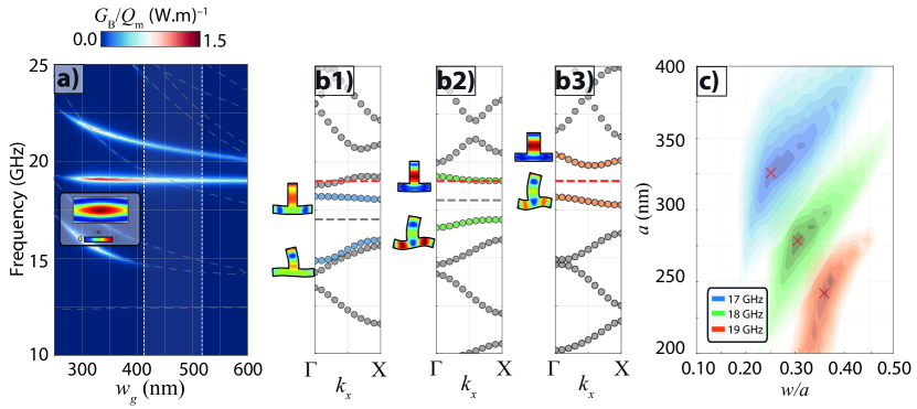
For BBS the design process has to be modified to carefully consider non zero . As discussed before the mechanical wave-vector is now coupled to the geometry via the optical dispersion Fig. 1 . To ease the bandgap search in this case, we fix the wave-vector for the mechanical simulations; this could be experimentally achieved by varying the optical frequency. In Fig. 3 (a) we evaluate the Brillouin optomechanical gain of a floating rectangular waveguide for intramodal BBS as a function of considering , the shaded region in the map is the width range where the optical frequency lies inside the photonic C-band and therefore can be easily adjusted.
BBS favors mechanical modes that have significant displacement in the -direction [40], and so the mode that yields the highest coupling factor is the -polarized L(1)-mode (Lamb-like), as seen in the inset of Fig. 4 (a). As discussed before, this is a hybrid mode with significant displacement in the and direction, and so a full bandgap is necessary to confine it to the BAR region. Full bandgaps are expected to be narrower, demanding for a finer design control over the bandgap central frequency and width, as seen in Fig. 3 (b). To obtain this level of control we consider one extra degree of freedom for the optimization: the filling factor (). Fig. 3 (c) shows the evolution of the bandgaps highlighted in Fig. 3 (b) considering both geometric parameters: and . Darker colors refers to larger bandgaps at the respective central frequency. By following the evolution of the bandgap position and size as a function of the central frequency we can easily choose the most appropriate parameters for the best confinement of the BAR mode.
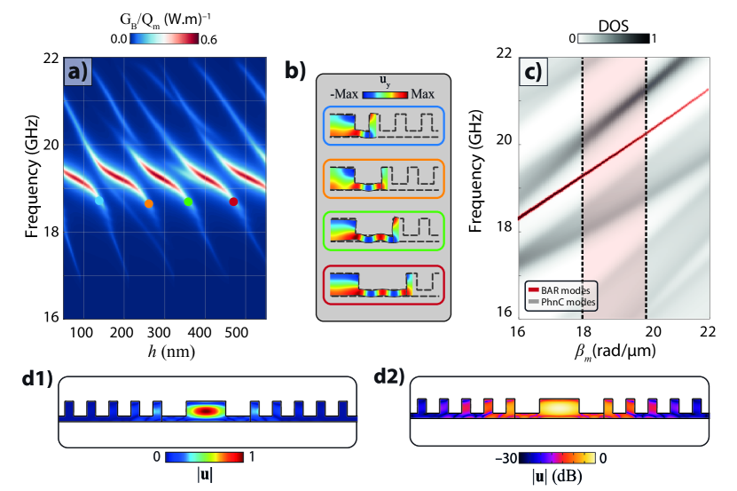
The Lamb-like mode is susceptible to crossings with the shear-vertical modes from the support due its small displacement in -direction. Considering the silicon bulk sound velocity we expect the support shear modes to have a wavelength of around . As a results, for every half wavelength increase in the support width () we expect to see a crossing of these two modes. This is precisely the origin for the anti-crossings seen in Fig. 4 (a), where we calculate the Brillouin optomechanical gain for the full waveguide structure at as a function of the width . The mechanical mode displacement profiles with low gain are shown in Fig. 4 (b) with size difference roughly equal to half the shear mode wavelength. The small discrepancy between the expected size difference and values recovered from the FEM simulations, occurs since the slab defined by does not have fixed boundary conditions at both ends, effectively increasing its width.
Now that the geometric parameters are set we can turn back our attention to the mechanical dispersion curves. In Fig. 4 (c) we have both the dispersion diagram of the PhnCC (shaded gray) and BAR modes (shaded red). The slope of the Lamb-like mode is close to shear modes, resulting in a small relative frequency shift between the defect and crystal modes. Therefore a mode well centered inside the bandgap for a given wave-vector, will then stay centered throughout a large range, this provides a tuning range for the mechanical frequency of for optical frequencies within the photonic C-band.
4 Discussion
Acoustic damping arises from three main sources: geometry dependent clamping losses, fabrication dependent resonance broadening [7, 39] and intrinsic mechanical losses [45, 46]. The latter is dominated by thermal effects such as Thermo-Elastic Damping (TED) and the Akhiezer Effect (AKE). Those are out of the scope of our design, but can be avoided in low-temperature experiments.
Mechanical clamping losses arises due to the lower acoustic velocity of the substrate material in comparison to the device material, in our design this effect is successfully suppressed by blinding the mechanical mode from the device-substrate interface. In both Breathing-like mode and Lamb-like mode, respectively shown in Fig. 2 and Fig. 4 , the mechanical displacement after only 5 PhnC cells was attenuated over 30 dB, this leads to radiation limited Q-factors of for the breathing-like and for the Lamb-like. Is important to note that those values are expected to increase exponentially with the addition of more cells [37].
The broadening of the Brillouin resonance due to fabrications defects have two length scales: the first being short-range variations, where broadening arises from surface roughness and composition, and the second being long-range where slow variations on the cross-section geometry lowers the mechanical coherence [39]. The first one should not limit the quality factor considering the ultra-high mechanical Q () already reported in silicon nanocavities at low temperatures [35]. In the second case its effect can be estimated by calculating the sensitivity of the mechanical frequency towards geometric variations. As expected the breathing-like mode is more sensitive to width variations () while the Lamb-like mode is more prone to height variations (). A table containing the sensitivity of the each mode towards different geometric parameters is presented in the Appendix A. Considering that the record width (height) variations on diameter wafer processing are on the order of () [47, 28] then the breathing(Lamb)-like the mechanical quality factor is limited at which would lead to a Brillouin Gain of . The calculation of the fabrication limited is discussed in appendix B.
An interesting comparison can be make between our design and the ideal fully suspended silicon nanowire with the same BAR dimensions. Tab. 1 presents both the coupling factor () and the dominant geometric sensitivity () for the two waveguides:
| Interaction | Waveguide | ||
|---|---|---|---|
| FBS | Fully Suspended | 10.91 | 21 |
| PhnC Assisted | 4.50 | 9 | |
| BBS | Fully Suspended | 0.83 | 48 |
| PhnC Assisted | 0.54 | 29 |
Even with the addition of the PhnCC the effective mechanical domain in our design is still larger than in the ideal case due to the connecting slab and the penetration depth of the mechanical mode inside the crystal. From the table above we can see that this increase manifest itself in two ways: a decrease in the Brillouin optomechanical coupling factor but also a decrease in the mechanical frequency sensitivity to changes in the geometry. If we consider that acoustic losses are limited by fabrication then we have (see Appendix B), meaning that the decrease in the coupling factor is balanced by the increase in the mechanical coherence, resulting in a Brillouin optomechanical Gain () that is effectively the same as the ideal case ( for FBS, for BBS). Our design then provides a feasible and robust structure, that can support itself over large lengths without halting the interaction, while still having the same gain performance of a fully suspended nanowires.
5 Conclusion
The presented waveguide design promotes an alternative approach for realizing SBS in silicon integrated waveguides. The addition of the mechanical shields (PhnCC) successfully mitigates mechanical clamping losses homogeneously throughout the propagation axis while still preserving the ease of fabrication. For both FBS and BBS optimized designs our waveguide possesses Brillouin Gain equivalent to fully suspended silicon nanowires with an additional advantage of long unperturbed interaction lengths making it ideal for interactions that possesses long acoustic decay lengths such as intramodal BBS. This approach could open the possibilities for the implementation of BBS based devices and high-frequency experiments in integrated silicon photonics. Our phonon shield design in principle could also enable the addition of electrical contacts without affecting too much on the mechanical mode. This could open novel applications such as thermal tuning, and p-i-n type structures that could lower the free-carrier lifetime and two-photon absorption in the waveguides [48]. Although we focus on silicon substrate, others material that suffer from mechanical clamping losses such as silicon nitride and gallium arsenide should also benefit from the presented design.
Data Availability
FEM and scripts files for generating each figure are available at the ZENODO repository (10.5281/zenodo.4148337) [49].
Funding
This work was supported by São Paulo Research Foundation (FAPESP) through grants 2019/13564-6, 2018/15580-6, 2018/15577-5, 2018/25339-4, Coordenação de Aperfeiçoamento de Pessoal de Nível Superior - Brasil (CAPES) (Finance Code 001), Conselho Nacional de Desenvolvimento Científico e Tecnológico through grants 425338/2018-5, 310224/2018-7, and Financiadora de Estudos e Projetos (Finep).
Appendix A: Sensitivity to dimensional variations
Inhomegenities over the waveguide cross section is one of the limiting factor for the Brillouin Resonance Quality factor, in order to calculate this limit is necessary to calculate each mode sensitivity to the dimensional variations. The sensitivities were calculated using COMSOL Multiphysics ® FEM simulations, we swept each parameter over a range and then linear fitting the mechanical frequency. In these simulations the optical wavelength was kept at . The table below show the sensitivities of the mechanical modes studied with respect to the dimensional parameters that should be more affected during the fabrication processes.
| Parameter | Mode | Sensitivty (MHz/nm) |
|---|---|---|
| Breathing-like | 8.70 | |
| Lamb-like | 5.74 | |
| Breathing-like | 3.86 | |
| Lamb-like | 5.94 | |
| Breathing-like | 0.81 | |
| Lamb-like | 28.92 |
Appendix B: Structural Broadening Calculations
The Brillouin gain over the stokes seed in a single-pass waveguide is given by the equation bellow:
| (2) |
As a result of the inhomogenities over the waveguide cross-section the frequency of the phase-matched mechanical mode is now a function of the longitudinal parameter . Considering that each parameter is perturbed over a mean value, the frequency can be written as:
| (3) |
where is the unperturbed frequency, is the perturbation over the dimensional parameter and is the frequency sensitivity related to the parameter. In a realistic approximation the dimensional variations are randomly distributed along the entire waveguide length with values within the tolerance of the fabrication procedure (). If the characteristic length of those variations is smaller than the effective length of the Brillouin interaction () and the pump power stays relatively constant throughout the length of the waveguide the above equation can be simplified, and the optical frequency offset () dependency then reads:
| (4) |
where is the probability of finding as that the frequency of the phase-matched mechanical mode at any given value of . The probability density function (PDF) of can be obtained by doing the convolution of the PDFs of every term in equation. Due to the nature of the convolution operation, Eq. 4 is dominated by the larger of the parameters . For a limit of vanishing intrinsic linewidth () the resulting linewidth tend to ().
References
- [1] R. W. Boyd, Nonlinear Optics (Elsevier, 2003).
- [2] E. P. Ippen and R. H. Stolen, “Stimulated Brillouin scattering in optical fibers,” \JournalTitleApplied Physics Letters (1972).
- [3] K. O. Hill, B. S. Kawasaki, and D. C. Johnson, “Cw Brillouin laser,” \JournalTitleApplied Physics Letters (1976).
- [4] N. L. Rowell, P. J. Thomas, H. M. Van Driel, and G. I. Stegeman, “Brillouin spectrum of single-mode optical fibers,” \JournalTitleApplied Physics Letters 34, 139–141 (1979).
- [5] P. T. Rakich, C. Reinke, R. Camacho, P. Davids, and Z. Wang, “Giant Enhancement of Stimulated Brillouin Scattering in the Subwavelength Limit,” \JournalTitlePhysical Review X 2, 011008 (2012).
- [6] G. S. Wiederhecker, P. Dainese, and T. P. M. Alegre, “Brillouin optomechanics in nanophotonic structures,” \JournalTitleAPL Photonics 4 (2019).
- [7] A. H. Safavi-Naeini, D. Van Thourhout, R. Baets, and R. Van Laer, “Controlling phonons and photons at the wavelength scale: integrated photonics meets integrated phononics: publisher’s note,” \JournalTitleOptica 6, 410 (2019).
- [8] B. J. Eggleton, C. G. Poulton, P. T. Rakich, M. J. Steel, and G. Bahl, “Brillouin integrated photonics,” \JournalTitleNature Photonics 13, 664–677 (2019).
- [9] R. Y. Chiao, C. H. Townes, and B. P. Stoicheff, “Stimulated Brillouin Scattering and Coherent Generation of Intense Hypersonic Waves,” \JournalTitlePhysical Review Letters 12, 592–595 (1964).
- [10] J. Xu, Y. Dong, Z. Zhang, S. Li, S. He, and H. Li, “Full scale strain monitoring of a suspension bridge using high performance distributed fiber optic sensors,” \JournalTitleMeasurement Science and Technology 27 (2016).
- [11] A. Zarifi, B. Stiller, M. Merklein, N. Li, K. Vu, D. Y. Choi, P. Ma, S. J. Madden, and B. J. Eggleton, “Highly localized distributed Brillouin scattering response in a photonic integrated circuit,” \JournalTitleAPL Photonics 3 (2018).
- [12] A. Byrnes, R. Pant, E. Li, D.-Y. Choi, C. G. Poulton, S. Fan, S. Madden, B. Luther-Davies, and B. J. Eggleton, “Photonic chip based tunable and reconfigurable narrowband microwave photonic filter using stimulated Brillouin scattering,” \JournalTitleOptics Express 20, 18836 (2012).
- [13] C. Feng, S. Preussler, and T. Schneider, “Sharp tunable and additional noise-free optical filter based on Brillouin losses,” \JournalTitlePhotonics Research 6, 132 (2018).
- [14] E. A. Kittlaus, S. Member, P. Kharel, N. T. Otterstrom, P. T. Rakich, and Z. Wang, “RF-Photonic Filters via On-Chip Photonic – Phononic Emit – Receive Operations,” \JournalTitleJournal of Lightwave Technology 36, 2803–2809 (2018).
- [15] A. Choudhary, Y. Liu, B. Morrison, K. Vu, D.-Y. Choi, P. Ma, S. Madden, D. Marpaung, and B. J. Eggleton, “High-resolution, on-chip RF photonic signal processor using Brillouin gain shaping and RF interference,” \JournalTitleScientific Reports 7, 5932 (2017).
- [16] H. Shin, J. A. Cox, R. Jarecki, A. Starbuck, Z. Wang, and P. T. Rakich, “Control of coherent information via on-chip photonic–phononic emitter–receivers,” \JournalTitleNature communications 6, 6427 (2015).
- [17] J. Li, M.-G. Suh, and K. Vahala, “Microresonator Brillouin gyroscope,” \JournalTitleOptica 4, 346 (2017).
- [18] I. S. Grudinin, A. B. Matsko, and L. Maleki, “Brillouin Lasing with a CaF\textsubscript{2} Whispering Gallery Mode Resonator,” \JournalTitlePhysical Review Letters 102, 043902 (2009).
- [19] M. Tomes and T. Carmon, “Photonic Micro-Electromechanical Systems Vibrating at X-band (11-GHz) Rates,” \JournalTitlePhysical Review Letters 102, 113601 (2009).
- [20] J. Li, H. Lee, T. Chen, and K. J. Vahala, “Characterization of a high coherence, Brillouin microcavity laser on silicon,” \JournalTitleOptics Express 20, 20170 (2012).
- [21] B. Morrison, A. Casas-Bedoya, G. Ren, K. Vu, Y. Liu, A. Zarifi, T. G. Nguyen, D.-Y. Choi, D. Marpaung, S. J. Madden, A. Mitchell, and B. J. Eggleton, “Compact Brillouin devices through hybrid integration on silicon,” \JournalTitleOptica 4, 847 (2017).
- [22] N. T. Otterstrom, R. O. Behunin, E. A. Kittlaus, Z. Wang, and P. T. Rakich, “A silicon Brillouin laser,” \JournalTitleScience 360, 1113–1116 (2018).
- [23] S. Gundavarapu, G. M. Brodnik, M. Puckett, T. Huffman, D. Bose, R. Behunin, J. Wu, T. Qiu, C. Pinho, N. Chauhan, J. Nohava, P. T. Rakich, K. D. Nelson, M. Salit, and D. J. Blumenthal, “Sub-hertz fundamental linewidth photonic integrated Brillouin laser,” \JournalTitleNature Photonics 13, 60–67 (2019).
- [24] R. Pant, A. Byrnes, C. G. Poulton, E. Li, D.-Y. Choi, S. Madden, B. Luther-Davies, and B. J. Eggleton, “Photonic-chip-based tunable slow and fast light via stimulated Brillouin scattering,” \JournalTitleOptics Letters 37, 969 (2012).
- [25] Y.-H. Lai, Y.-K. Lu, M.-G. Suh, Z. Yuan, and K. Vahala, “Observation of the exceptional-point-enhanced Sagnac effect,” \JournalTitleNature 576, 65–69 (2019).
- [26] H. Wang, Y.-H. Lai, Z. Yuan, M.-G. Suh, and K. Vahala, “Petermann-factor sensitivity limit near an exceptional point in a Brillouin ring laser gyroscope,” \JournalTitleNature Communications 11, 1610 (2020).
- [27] F. Gyger, J. Liu, F. Yang, J. He, A. S. Raja, R. N. Wang, S. A. Bhave, T. J. Kippenberg, and L. Thévenaz, “Observation of Stimulated Brillouin Scattering in Silicon Nitride Integrated Waveguides,” \JournalTitlePhys. Rev. Lett. 124, 13902 (2020).
- [28] R. Van Laer, B. Kuyken, D. Van Thourhout, and R. Baets, “Interaction between light and highly confined hypersound in a silicon photonic nanowire,” \JournalTitleNature Photonics 9, 199–203 (2015).
- [29] I. V. Kabakova, R. Pant, D.-Y. Choi, S. Debbarma, B. Luther-Davies, S. J. Madden, and B. J. Eggleton, “Narrow linewidth Brillouin laser based on chalcogenide photonic chip,” \JournalTitleOptics letters 38, 3208–3211 (2013).
- [30] R. Van Laer, A. Bazin, B. Kuyken, R. Baets, and D. Van Thourhout, “Net on-chip Brillouin gain based on suspended silicon nanowires,” \JournalTitleNew Journal of Physics 17, 115005 (2015).
- [31] E. A. Kittlaus, H. Shin, and P. T. Rakich, “Large Brillouin amplification in silicon,” \JournalTitleNature Photonics 10, 463–467 (2016).
- [32] E. A. Kittlaus, N. T. Otterstrom, and P. T. Rakich, “On-chip inter-modal Brillouin scattering,” \JournalTitleNature communications 8, 15819 (2017).
- [33] C. Wolff, M. J. Steel, B. J. Eggleton, and C. G. Poulton, “Acoustic build-up in on-chip stimulated Brillouin scattering,” \JournalTitleScientific Reports 5, 13656 (2015).
- [34] W. H. Renninger, P. Kharel, R. O. Behunin, and P. T. Rakich, “Bulk crystalline optomechanics,” \JournalTitleNature Physics 14, 601–607 (2018).
- [35] G. S. MacCabe, H. Ren, J. Luo, J. D. Cohen, H. Zhou, A. Sipahigil, M. Mirhosseini, and O. Painter, “Phononic bandgap nano-acoustic cavity with ultralong phonon lifetime,” \JournalTitlearXiv pp. 1–43 (2019).
- [36] H. Ren, M. H. Matheny, G. S. MacCabe, J. Luo, H. Pfeifer, M. Mirhosseini, and O. Painter, “Two-dimensional optomechanical crystal cavity with high quantum cooperativity,” \JournalTitleNature Communications 11, 3373 (2020).
- [37] F. G. S. Santos, Y. A. V. Espinel, G. O. Luiz, R. S. Benevides, G. S. Wiederhecker, and T. P. M. Alegre, “Hybrid confinement of optical and mechanical modes in a bullseye optomechanical resonator,” \JournalTitleOptics express 25, 508–529 (2017).
- [38] R. Dehghannasiri, A. A. Eftekhar, and A. Adibi, “Raman-like stimulated Brillouin scattering in phononic-crystal-assisted silicon-nitride waveguides,” \JournalTitlePhysical Review A (2017).
- [39] C. Wolff, R. Van Laer, M. J. Steel, B. J. Eggleton, and C. G. Poulton, “Brillouin resonance broadening due to structural variations in nanoscale waveguides,” \JournalTitleNew Journal of Physics 18 (2016).
- [40] Y. A. V. Espinel, F. G. S. Santos, G. O. Luiz, T. P. M. Alegre, and G. S. Wiederhecker, “Brillouin Optomechanics in Coupled Silicon Microcavities,” \JournalTitleScientific Reports 7, 43423 (2017).
- [41] W. B. Fraser, “Stress wave propagation in rectangular bars,” \JournalTitleInternational Journal of Solids and Structures 5, 379–397 (1969).
- [42] A. A. Krushynska and V. V. Meleshko, “Normal waves in elastic bars of rectangular cross section,” \JournalTitleThe Journal of the Acoustical Society of America 129, 1324–1335 (2011).
- [43] R. Benevides, F. G. S. Santos, G. O. Luiz, G. S. Wiederhecker, and T. P. M. Alegre, “Ultrahigh-Q optomechanical crystal cavities fabricated in a CMOS foundry,” \JournalTitleScientific Reports 7, 2491 (2017).
- [44] M. A. Tran, D. Huang, T. Komljenovic, J. Peters, A. Malik, and J. E. Bowers, “Ultra-low-loss silicon waveguides for heterogeneously integrated silicon/III-V photonics,” \JournalTitleApplied Sciences (Switzerland) 8 (2018).
- [45] C. Zener, “Internal Friction in Solids II. General Theory of Thermoelastic Internal Friction,” \JournalTitlePhysical Review 53, 90–99 (1938).
- [46] E. Chávez-Ángel, R. A. Zarate, J. Gomis-Bresco, F. Alzina, and C. M. Sotomayor Torres, “Modification of Akhieser mechanism in Si nanomembranes and thermal conductivity dependence of the Q -factor of high frequency nanoresonators,” \JournalTitleSemiconductor Science and Technology 29, 124010 (2014).
- [47] S. K. Selvaraja, P. De Heyn, G. Winroth, P. Ong, G. Lepage, C. Cailler, A. Rigny, K. K. Bourdelle, W. Bogaerts, D. Van Thourhout, J. Van Campenhout, and P. Absil, “Highly uniform and low-loss passive silicon photonics devices using a 300mm CMOS platform,” in Optical Fiber Communication Conference, (OSA, Washington, D.C., 2014), 1, p. Th2A.33.
- [48] A. Gajda, L. Zimmermann, J. Bruns, B. Tillack, and K. Petermann, “Design rules for p-i-n diode carriers sweeping in nano-rib waveguides on SOI,” \JournalTitleOptics Express (2011).
- [49] R. O. Zurita, G. S. Wiederhecker, and T. P. M. Alegre, “Dataset and simulation files for article: "Designing of strongly confined short-wave Brillouin phonons in silicon waveguide periodic lattices"".” .