Tunable interdot coupling in few-electron bilayer graphene double quantum dots
Abstract
We present a highly controllable double quantum dot device based on bilayer graphene. Using a device architecture of interdigitated gate fingers, we can control the interdot tunnel coupling between 1 to 4 GHz and the mutual capacitive coupling between 0.2 and 0.6 meV, independently of the charge occupation of the quantum dots. The charging energy and hence the dot size remains nearly unchanged. The tuning range of the tunnel coupling covers the operating regime of typical silicon and GaAs spin qubit devices.
Spin qubits implemented in semiconductor quantum dots (QDs) are attractive candidates for enabling solid state quantum computing Loss and DiVincenzo (1998); Yoneda et al. (2017); Watson et al. (2018). In particular, singlet-triplet spin qubits, where the logical qubits are encoded in a two-electron spin system in double quantum dots (DQDs) turned out to be very interesting as they allow fast quantum gate operations avoiding fast microwave pulses Petta et al. (2005); Foletti et al. (2009); Barthel et al. (2012); Wu et al. (2014); Takeda et al. (2020). For such qubit systems control over the interdot tunnel coupling and hence the exchange interaction between the electrons in the two coupled QDs is essential Levy (2002); Martins et al. (2016); Reed et al. (2016); Takeda et al. (2020). Typical tunnel coupling energies are on the order of 1 GHz for silicon- Wu et al. (2014) and up to 3 GHz for GaAs-based Barthel et al. (2012) spin qubits allowing fast quantum gate operations.
Bilayer graphene (BLG) is an attractive host material for spin qubits due to its small spin-orbit and hyperfine interaction, as well as the possibility to open a gate voltage controllable band gap Trauzettel et al. (2007); Oostinga et al. (2007); Zhang et al. (2009). The development of ultra-clean van der Waals heterostructures where a BLG sheet is encapsulated in hexagonal boron nitride (hBN) Wang et al. (2013) and a graphite crystal is used as a back gate Overweg et al. (2018) has lead to a boost in device quality and has enabled the implementation of well-defined QDs Eich et al. (2018a); Kurzmann et al. (2019); Banszerus et al. (2020a); Tong et al. (2020); Banszerus et al. (2020b) and DQDs Eich et al. (2018b); Banszerus et al. (2018, 2020c). The device architecture used so far to study the single- to few-electron regime in BLG DQDs is based on one gate per QD, where the interdot tunnel barrier is tuned by stray fields of the dot-defining gates Banszerus et al. (2020c). This inhibits the independent control of the interdot tunneling barriers and the charge occupation of the QDs. The implementation of separate gates, one controlling the dot occupation and one controlling the tunnel coupling, is also possible for BLG QD devices Eich et al. (2018b); Tong et al. (2020) and is a well-established technique in different types of GaAs-based QD devices Medford et al. (2013); Takakura et al. (2014); Volk et al. (2019); Hsiao et al. (2020). In electron and hole QD systems based on SiMOS, Si/SiGe and Ge/SiGe heterostructures, an additional gate layer implementing interdigitated finger gates has been used for that purpose Yang et al. (2014); Zajac et al. (2015); Liles et al. (2018); Eenink et al. (2019); Lawrie et al. (2020).
Here, we show independent gate control of the tunnel coupling and the mutual capacitive coupling in a few-electron bilayer graphene double quantum dot device while keeping the dot occupations and the dot size, i.e. the charging energy, constant. In short, we demonstrate the operation of an advanced device architecture with interdigitated gate fingers that allows for a precise modulation of the band edge profile defining the confinement potential and tunneling rates.
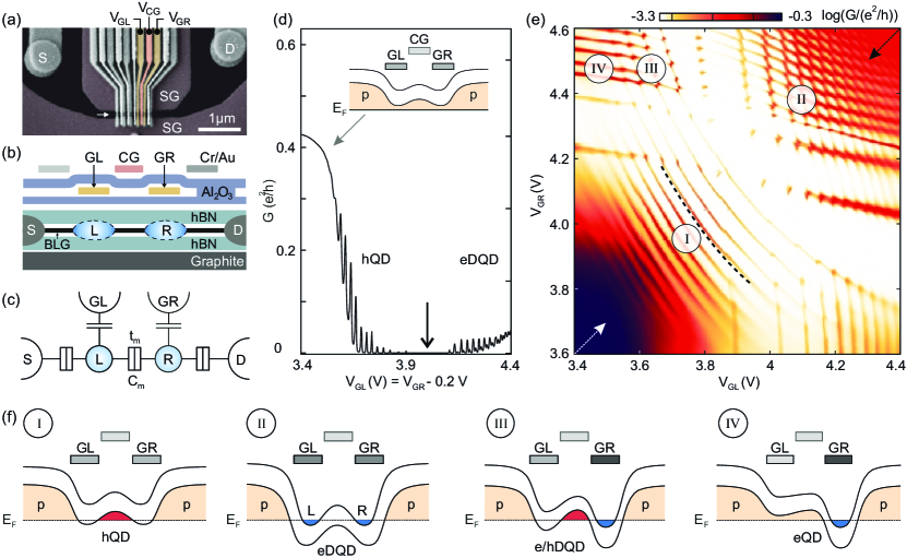
Fig. 1(a) shows a scanning electron micrograph of a fabricated device. It consists of a BLG flake, which has been encapsulated between two crystals of hexagonal boron nitride of approximately 25 nm thickness using conventional dry van-der-Waals stacking techniques Engels et al. (2014); Wang et al. (2013). The heterostructure is placed on a graphite flake, acting as a back gate Banszerus et al. (2018). One-dimensional Cr/Au side contacts are used as ohmic contacts to the BLG Wang et al. (2013). On top of this stack, we deposit metallic split gates (lateral separation of 130 nm) by electron beam lithography, metal evaporation of (5 nm Cr/30 nm Au), and lift-off. Separated from the split gates by a thick layer of atomic layer deposited (ALD) , we fabricate wide finger gates (FGs) with a pitch of . We use the precursors Trimethylaluminium and H2O in the ALD process and avoid plasma assisted ALD as an O2 plasma can attack the hBN. To avoid ungated regions along the channel, we fabricate a second layer of FGs, with same width and pitch, separated from the first one by an additional layer of . A schematic cross section through the heterostructure and the gate stack is shown in Fig. 1(b) where the positions of the left (L) and right (R) QD are highlighted. Fig. 1(c) shows a simplified circuit diagram of a DQD. All measurements are performed in a dilution refrigerator at a base temperature of and an electron temperature of around , using standard DC measurement techniques. We use a home-built IV-converter with a gain of and a bandwidth of 600 Hz to measure currents in the sub-pA regime. To characterize the BLG, we perform quantum Hall measurements (not shown). We extract a residual doping of cm-2, a charge carrier density inhomogeneiety of cm-2 and a quantum mobility exceeding cm2/(Vs).
In order to form QDs in the extended BLG sheet, we first define a narrow conductive channel by opening a displacement field induced band gap underneath the split gates. For this, we apply a constant back gate voltage of and a split gate voltage of resulting in a band gap of around 30 meV in the regions below the SGs and an overall p-doped channel. Second, we make use of the individual FGs to locally tune the band edges of the gapped BLG with respect to the Fermi level. For example, when applying a positive voltage on both finger gates GL and GR – while keeping all other FGs at 0 V – we tune the band edges such that tunneling barriers form below GL and GR allowing to fully suppress transport through the channel. This is verified by the conductance trace shown in Fig. 1(d) (see black arrow). For smaller finger gate voltages, we observe regular Coulomb resonances, which we attribute to a hole QD (hQD) below CG, as for large gate voltages we enter the regime of an electron DQD (eDQD).
The different transport regimes become more apparent when investigating the conductance as a function of and (see Fig. 1(e)); the dashed arrows mark the cross-section shown in Fig. 1(d). In this charge stability diagram, we highlight the different transport regimes (see labels I, II, III and IV; corresponding schematics of the band edge diagrams are shown in Fig. 1(f)).
At low voltages around and (regime I), we observe hyperbolically shaped charge addition lines indicating the presence of a single hole QD (see dashed line in Fig. 1(e)). Increasing both gate voltages, the hole QD is depleted more and more due to the capacitive cross-talk of these gates to the QD and we observe the transition to an electron DQD (regime II). The DQD regime shows the characteristic hexagonal pattern of the charge addition lines and extends over a wide voltage range before the increasing tunnel coupling leads to the transition to a single QD. Interestingly, in an intermediate region, an ambipolar triple QD is formed, where the outer two QDs are occupied by one electron and the inner QD by a single hole.
Furthermore, we can manipulate the band edges to form different ambipolar DQD configurations. In regime III ( and ), a hole-electron ambipolar DQD is formed where the horizontal lines indicate charge transitions of the electron QD while the curved lines show transitions of the hole QD. A further reduction of at constant lifts the tunnel barrier separating the hole QD from the left reservoir leaving only a single electron QD below the right gate (regime IV). The opposite charge configuration can be observed in the bottom right of the shown charge stability diagram. This measurement proves the versatility of the device which allows smooth transitions between unipolar and ambipolar QD configurations. Consistent results were also obtained from QD configurations formed by a different pair of finger gates. The pinch off voltages of the gates in the first finger gate layer (5 out of 6 gates worked) show a spread of V.
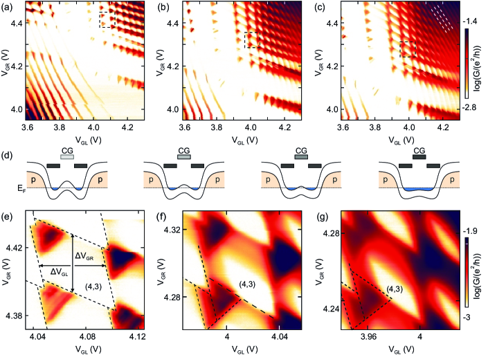
In the following, we focus on the interdot coupling of the electron DQD (regime II). In order to study the influence of the central gate (CG) located in the second finger gate layer between the gates GL and GR, we measure charge stability diagrams for different (see Fig. 2(a)-(c)). Two significant effects can be observed: First, all DQD and hole dot transitions in the charge stability diagram are shifted towards lower and values with increasing due to cross capacitances of the CG and the two QDs. Second, the interdot tunnel coupling in the DQD regime increases as the conduction band edge is pushed more and more towards the Fermi level. This effect is illustrated in the schematics shown in Fig. 2(d). At high (and high and ), the tunneling barrier is lifted fully, eventually leading to the formation of a large single QD which manifests in the appearance of diagonal charge addition lines (see e.g. dashed lines in Fig. 2(c)). Fig. 2(e)-(g) show close-ups of the few electron DQD regime (around the occupation of (4,3) electrons; see dashed rectangles in Fig. 2(a)-(c)). Qualitatively, the effect of increasing interdot tunnel coupling becomes apparent by the broadening of features within the triple points, as well as by the significantly enhanced conductivity along the co-tunneling lines.
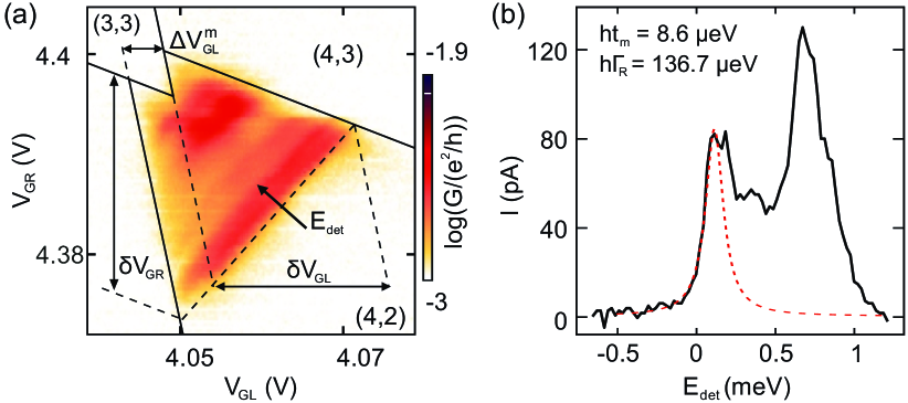
For a quantitative analysis of the impact of the central gate on the interdot coupling and the QD size, we determine the mutual capacitive coupling energy , the interdot tunnel coupling , and the charging energies as a function of . Fig. 3(a) shows the charge stability diagram of an individual pair of triple points highlighting the relevant quantities to extract and . We determine the charging energy of each of the QDs from the charge stability diagrams as shown in Figs. 2(e)-(g) according to with the lever arms . The mutual capacitive coupling energy is given by Volk et al. (2011). The interdot tunnel coupling can be extracted from current traces recorded along the detuning energy () axis (see e.g. black arrow in Fig. 3(a)). A representative measurement is shown in Fig. 3(b), where the detuning axis corresponds to a cut through the triple point shown in Fig. 3(a). Resonances inside the triple point are clearly visible, which correspond to transport involving excited states. We fit the current through the ground state according to a model assuming a Lorentzian line shape Fringes et al. (2012); Liu et al. (2010); van der Wiel et al. (2002); Stoof and Nazarov (1996) resulting in the limit of to
| (1) |
where are the tunnel rates to the left and right lead, respectively.
The results of the detailed analysis are summarized in Fig. 4. Fig. 4(a) shows that the mutual capacitive coupling increases monotonically with , which can be explained by the fact that the two electron QDs (L and R) are pushed closer to each other for increasing (see sequence shown in Fig. 2(d)). This results in an increase of and thus to an increase of . Consistently, for lower dot occupations this effect is slightly less pronounced resulting in a lower increase. The observed monotonic behaviour is in contrast to earlier work on a physically etched single-layer graphene DQD Molitor et al. (2009) and on a gate-defined DQD in an etched graphene nanoribbon Liu et al. (2010), which showed a non-monotonous dependency of on the gate voltage. Furthermore, in etched BLG DQDs, increased or decreased with the gate voltage depending an the charge occupation of the DQD Volk et al. (2011); Fringes et al. (2012).
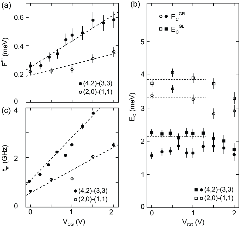
Fig. 4(b) shows that has rather little effect on the charging energy and hence the size of the QDs. From a simplified plate capacitor model approximating the QDs as discs separated from the back gate by 25 nm of hBN, we determine upper limits for the effective QD diameters nm and nm in the few electron regime and nm and nm in the low electron regime. These estimates are in reasonable agreement with the lithographic dimensions. The pitch of the plunger gates measures 150 nm and the split gates are separated by around 130 nm.
Finally, in Fig. 4(c), we show the tunnel coupling for a fixed charge carrier occupation for different gate voltages . We show that can be tuned monotonously in the range from 1 to 4 GHz at the (4,2)-(3,3) transition and from 0.7 to 2.5 GHz at the (2,0)-(1,1) transition covering the operating regime for silicon and GaAs spin qubit devices Wu et al. (2014); Barthel et al. (2012).For larger the double dot merges into one large single QD, c.f. higher charge occupation in Fig. 1e).
In conclusion, we studied a BLG QD system where we introduced a second layer of finger gates forming a dense pattern of gates.
We focus on an electron DQD where two dedicated finger gates act as plunger gates controlling the number of charge carriers on each of the QDs from the few-electron regime down to the very last electron. An additional gate, positioned in between those, controls the interdot coupling. Tuning the interdot tunnel coupling in the range of 1 to 4 GHz at a constant charge occupation meets a basic requirement making BLG QD arrays suitable building block for spin qubit devices, which brings BLG closer as a serious quantum technology platform.
Acknowledgements The authors thank S. Trellenkamp, F. Lentz and D. Neumaier for their support in device fabrication.
This project has received funding from the European Union’s Horizon 2020 research and innovation programme under grant agreement No. 881603 (Graphene Flagship) and from the European Research Council (ERC) under grant agreement No. 820254, the Deutsche Forschungsgemeinschaft (DFG, German Research Foundation) under Germany’s Excellence Strategy - Cluster of Excellence Matter and Light for Quantum Computing (ML4Q) EXC 2004/1 - 390534769, through DFG (STA 1146/11-1), and by the Helmholtz Nano Facility Albrecht et al. (2017). Growth of hexagonal boron nitride crystals was supported by the Elemental Strategy Initiative conducted by the MEXT, Japan, Grant Number JPMXP0112101001, JSPS KAKENHI Grant Numbers JP20H00354 and the CREST(JPMJCR15F3), JST.
Data availability The data that support the findings of this study are available from the corresponding author upon reasonable request.
References
- Loss and DiVincenzo (1998) D. Loss and D. P. DiVincenzo, Phys. Rev. A 57, 120 (1998).
- Yoneda et al. (2017) J. Yoneda, K. Takeda, T. Otsuka, T. Nakajima, M. R. Delbecq, G. Allison, T. Honda, T. Kodera, S. Oda, Y. Hoshi, N. Usami, K. M. Itoh, and S. Tarucha, Nat. Nanotechnol. 13, 102 (2017).
- Watson et al. (2018) T. F. Watson, S. G. J. Philips, E. Kawakami, D. R. Ward, P. Scarlino, M. Veldhorst, D. E. Savage, M. G. Lagally, M. Friesen, S. N. Coppersmith, M. A. Eriksson, and L. M. K. Vandersypen, Nature 555, 633 (2018).
- Petta et al. (2005) J. R. Petta, A. C. Johnson, J. M. Taylor, E. A. Laird, A. Yacoby, M. D. Lukin, C. M. Marcus, M. P. Hanson, and A. C. Gossard, Science 309, 2180 (2005).
- Foletti et al. (2009) S. Foletti, H. Bluhm, D. Mahalu, V. Umansky, and A. Yacoby, Nat. Phys. 5, 903 (2009).
- Barthel et al. (2012) C. Barthel, J. Medford, H. Bluhm, A. Yacoby, C. M. Marcus, M. P. Hanson, and A. C. Gossard, Phys. Rev. B 85, 035306 (2012).
- Wu et al. (2014) X. Wu, D. R. Ward, J. R. Prance, D. Kim, J. K. Gamble, R. T. Mohr, Z. Shi, D. E. Savage, M. G. Lagally, M. Friesen, S. N. Coppersmith, and M. A. Eriksson, Proc. Natl. Acad. Sci. U.S.A. 111, 11938 (2014).
- Takeda et al. (2020) K. Takeda, A. Noiri, J. Yoneda, T. Nakajima, and S. Tarucha, Phys. Rev. Lett. 124, 117701 (2020).
- Levy (2002) J. Levy, Phys. Rev. Lett. 89, 147902 (2002).
- Martins et al. (2016) F. Martins, F. K. Malinowski, P. D. Nissen, E. Barnes, S. Fallahi, G. C. Gardner, M. J. Manfra, C. M. Marcus, and F. Kuemmeth, Phys. Rev. Lett. 116, 116801 (2016).
- Reed et al. (2016) M. D. Reed, B. M. Maune, R. W. Andrews, M. G. Borselli, K. Eng, M. P. Jura, A. A. Kiselev, T. D. Ladd, S. T. Merkel, I. Milosavljevic, E. J. Pritchett, M. T. Rakher, R. S. Ross, A. E. Schmitz, A. Smith, J. A. Wright, M. F. Gyure, and A. T. Hunter, Phys. Rev. Lett. 116, 110402 (2016).
- Trauzettel et al. (2007) B. Trauzettel, D. V. Bulaev, D. Loss, and G. Burkard, Nat. Phys. 3, 192 (2007).
- Oostinga et al. (2007) J. B. Oostinga, H. B. Heersche, X. Liu, A. F. Morpurgo, and L. M. K. Vandersypen, Nat. Mater. 7, 151 (2007).
- Zhang et al. (2009) Y. Zhang, T.-T. Tang, C. Girit, Z. Hao, M. C. Martin, A. Zettl, M. F. Crommie, Y. R. Shen, and F. Wang, Nature 459, 820 (2009).
- Wang et al. (2013) L. Wang, I. Meric, P. Y. Huang, Q. Gao, Y. Gao, H. Tran, T. Taniguchi, K. Watanabe, L. M. Campos, D. A. Muller, J. Guo, P. Kim, J. Hone, K. L. Shepard, and C. R. Dean, Science 342, 614 (2013).
- Overweg et al. (2018) H. Overweg, H. Eggimann, X. Chen, S. Slizovskiy, M. Eich, R. Pisoni, Y. Lee, P. Rickhaus, K. Watanabe, T. Taniguchi, V. Fal’ko, T. Ihn, and K. Ensslin, Nano Lett. 18, 553 (2018).
- Eich et al. (2018a) M. Eich, R. Pisoni, H. Overweg, A. Kurzmann, Y. Lee, P. Rickhaus, T. Ihn, K. Ensslin, F. Herman, M. Sigrist, K. Watanabe, and T. Taniguchi, Phys. Rev. X 8, 031023 (2018a).
- Kurzmann et al. (2019) A. Kurzmann, M. Eich, H. Overweg, M. Mangold, F. Herman, P. Rickhaus, R. Pisoni, Y. Lee, R. Garreis, C. Tong, K. Watanabe, T. Taniguchi, K. Ensslin, and T. Ihn, Phys. Rev. Lett. 123, 026803 (2019).
- Banszerus et al. (2020a) L. Banszerus, T. Fabian, S. Möller, E. Icking, H. Heiming, S. Trellenkamp, F. Lentz, D. Neumaier, M. Otto, K. Watanabe, T. Taniguchi, F. Libisch, C. Volk, and C. Stampfer, Phys. Status Solidi B 257, 2000333 (2020a).
- Tong et al. (2020) C. Tong, R. Garreis, A. Knothe, M. Eich, A. Sacchi, K. Watanabe, T. Taniguchi, V. Fal’ko, T. Ihn, K. Ensslin, and A. Kurzmann, arXiv (2020), 2009.04337 .
- Banszerus et al. (2020b) L. Banszerus, A. Rothstein, T. Fabian, S. Möller, E. Icking, S. Trellenkamp, F. Lentz, D. Neumaier, K. Watanabe, T. Taniguchi, F. Libisch, C. Volk, and C. Stampfer, Nano Lett. 20, 7709 (2020b).
- Eich et al. (2018b) M. Eich, R. Pisoni, A. Pally, H. Overweg, A. Kurzmann, Y. Lee, P. Rickhaus, K. Watanabe, T. Taniguchi, K. Ensslin, and T. Ihn, Nano Lett. 18, 5042 (2018b).
- Banszerus et al. (2018) L. Banszerus, B. Frohn, A. Epping, D. Neumaier, K. Watanabe, T. Taniguchi, and C. Stampfer, Nano Lett. 18, 4785 (2018).
- Banszerus et al. (2020c) L. Banszerus, S. Möller, E. Icking, K. Watanabe, T. Taniguchi, C. Volk, and C. Stampfer, Nano Lett. 20, 2005 (2020c).
- Medford et al. (2013) J. Medford, J. Beil, J. M. Taylor, E. I. Rashba, H. Lu, A. C. Gossard, and C. M. Marcus, Phys. Rev. Lett. 111, 050501 (2013).
- Takakura et al. (2014) T. Takakura, A. Noiri, T. Obata, T. Otsuka, J. Yoneda, K. Yoshida, and S. Tarucha, Appl. Phys. Lett. 104, 113109 (2014).
- Volk et al. (2019) C. Volk, A. M. J. Zwerver, U. Mukhopadhyay, P. T. Eendebak, C. J. van Diepen, J. P. Dehollain, T. Hensgens, T. Fujita, C. Reichl, W. Wegscheider, and L. M. K. Vandersypen, npj Quantum Inf. 5, 1 (2019).
- Hsiao et al. (2020) T.-K. Hsiao, C. J. van Diepen, U. Mukhopadhyay, C. Reichl, W. Wegscheider, and L. M. K. Vandersypen, Phys. Rev. Appl. 13, 054018 (2020).
- Yang et al. (2014) C. H. Yang, A. Rossi, N. S. Lai, R. Leon, W. H. Lim, and A. S. Dzurak, Appl. Phys. Lett. 105, 183505 (2014).
- Zajac et al. (2015) D. M. Zajac, T. M. Hazard, X. Mi, K. Wang, and J. R. Petta, Appl. Phys. Lett. 106, 223507 (2015).
- Liles et al. (2018) S. D. Liles, R. Li, C. H. Yang, F. E. Hudson, M. Veldhorst, A. S. Dzurak, and A. R. Hamilton, Nat. Commun. 9, 1 (2018).
- Eenink et al. (2019) H. G. J. Eenink, L. Petit, W. I. L. Lawrie, J. S. Clarke, L. M. K. Vandersypen, and M. Veldhorst, Nano Lett. 19, 8653 (2019).
- Lawrie et al. (2020) W. I. L. Lawrie, H. G. J. Eenink, N. W. Hendrickx, J. M. Boter, L. Petit, S. V. Amitonov, M. Lodari, B. Paquelet Wuetz, C. Volk, S. G. J. Philips, G. Droulers, N. Kalhor, F. van Riggelen, D. Brousse, A. Sammak, L. M. K. Vandersypen, G. Scappucci, and M. Veldhorst, Appl. Phys. Lett. 116, 080501 (2020).
- Engels et al. (2014) S. Engels, B. Terrés, A. Epping, T. Khodkov, K. Watanabe, T. Taniguchi, B. Beschoten, and C. Stampfer, Phys. Rev. Lett. 113, 126801 (2014).
- Volk et al. (2011) C. Volk, S. Fringes, B. Terrés, J. Dauber, S. Engels, S. Trellenkamp, and C. Stampfer, Nano Lett. 11, 3581 (2011).
- Fringes et al. (2012) S. Fringes, C. Volk, B. Terrés, J. Dauber, S. Engels, S. Trellenkamp, and C. Stampfer, Phys. Status solidi C 9, 169 (2012).
- Liu et al. (2010) X. L. Liu, D. Hug, and L. M. K. Vandersypen, Nano Lett. 10, 1623 (2010).
- van der Wiel et al. (2002) W. G. van der Wiel, S. De Franceschi, J. M. Elzerman, T. Fujisawa, S. Tarucha, and L. P. Kouwenhoven, Rev. Mod. Phys. 75, 1 (2002).
- Stoof and Nazarov (1996) T. H. Stoof and Yu. V. Nazarov, Phys. Rev. B 53, 1050 (1996).
- Molitor et al. (2009) F. Molitor, S. Dröscher, J. Güttinger, A. Jacobsen, C. Stampfer, T. Ihn, and K. Ensslin, Appl. Phys. Lett. 94, 222107 (2009).
- Albrecht et al. (2017) W. Albrecht, J. Moers, and B. Hermanns, Journal of Large-Scale Research Facilities 3, 112 (2017).