A flux tunable superconducting quantum circuit based on Weyl semimetal MoTe2
Abstract
Weyl semimetals for their exotic topological properties have drawn considerable attention in many research fields. When in combination with s-wave superconductors, the supercurrent can be carried by their topological surface channels, forming junctions mimic the behavior of Majorana bound states. Here, we present a transmon-like superconducting quantum intereference device (SQUID) consists of lateral junctions made of Weyl semimetal Td-MoTe2 and superconducting leads niobium nitride (NbN). The SQUID is coupled to a readout cavity made of molybdenum rhenium (MoRe), whose response at high power reveal the existence of the constituting Josephson junctions (JJs). The loop geometry of the circuit allows the resonant frequency of the readout cavity to be tuned by the magnetic flux. We demonstrate a JJ made of MoTe2 and a flux-tunable transmon-like circuit based on Weyl materials. Our study provides a platform to utilize topological materials in SQUID-based quantum circuits for potential applications in quantum information processing.
I I. Introduction
Weyl semimetals are three-dimensional phases of matter with gapless band structures that are protected by topology and symmetry Armitage et al. (2018). The low-energy bands in Weyl semimetals can be viewed as a three-dimensional version of graphene, i.e., dispersing linearly along all the three momentum directions across the Weyl points (WPs). The WPs always appear in pairs with opposite chirality, and are connected by open curve-like Fermi surfaces with nondegenerate spin texture, as known as surface Fermi arcs Armitage et al. (2018). Recently, orthorhombic Td-phase transition metal dichalcogenides (such as WTe2 and MoTe2) have been predicted to be type-II Weyl semimetals Soluyanov et al. (2015); Chang et al. (2016), which is later supported by several experimental studies Jiang et al. (2017); Li et al. (2017). In addition, the topologically protected surface states of Weyl semimetals are expected to transmit electrical currents without backscattering, and therefore could provide a robust weak link to carry supercurrent in Josephson junctions (JJ). A recent study on a lateral junction made of Td-WTe2 has shown a nontrivial temperature dependence of critical current (), in which a short junction behavior was observed in a long junction device Shvetsov et al. (2018). The long-lived temperature dependence of () has been attributed to the topologically protected surface Fermi arc states in Weyl semimetal Shvetsov et al. (2018). In another study, a missing =1 step, indicating the existence of the nontrivial 4-periodic supercurrent, was observed in a nanowire JJ made of Dirac semimetal Cd3As2 and is also attributed to its surface Fermi arc states Wang et al. (2018). On the other hand, integrating 2D materials (such as graphene) with superconducting circuits is an emerging topic in searching of new types of quantum computing devices owing to its superb conductivity and 2D gateable nature Casparis et al. (2018); Chiu (2018); Kroll et al. (2018); Wang et al. (2019). Several key observations, such as gate-tunable qubit energy Kroll et al. (2018); Wang et al. (2019), Rabi oscillation and qubit relaxation time (dephasing time ) at the scale of 36 ns (51 ns), have been reported Wang et al. (2019).
Topological materials, for their topologically protected surface and edge states which can serve as a robust channel to carry supercurrent, are also promising candidates for use in 2D materials-based quantum computing devices Chiu and Xu (2017); Chien et al. (2020). Recently, a topological insulator nanoribbon has been reported for use in superconducting quantum circuits Schmitt (2020). In addition, the S-T-S junction (S is superconductor and T is topological material) naturally provides a platform to explore the physics associated with Majorana bound states (MBS) Fu and Kane (2009, 2008); Badiane et al. (2013). In this letter, we explore a flux-tunable superconducting quantum intereference device (SQUID) consists of Weyl semimetal Td-MoTe2 and superconducting leads niobium nitride (NbN). The S-T-S junction is capacitively coupled to a superconducting readout cavity made of molybdenum rhenium (MoRe), with an intended design similar to a transmon. The power dependence of the readout cavity frequency demonstrates the successfully fabricated JJs while the flux-tunability of that reveal a symmetric DC SQUID. We compare our results with a theoretical framework where 4-periodic supercurrent plays a role in a topological junction. Our results demonstrate a flux-tunable DC SQUID based on Weyl semimetal and the integration with readout cavity provides a platform for potential applications in quantum information processing.
II II. Device fabrication and measurement setup
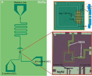
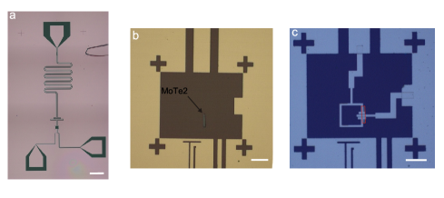
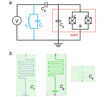
Fig. 1 shows the geometry of the SQUID along with the surrounding superconducting quantum circuits in our device. The SQUID is made of two NbN-MoTe2-NbN junctions, with a enclosed loop defined by a square (18 18 ) of NbN. The SQUID is shunted by a capacitor formed between a T-shape island and the surrounding ground, which are made by MoRe. The SQUID and shunting capacitor is equipped with three other components: a reflective microwave readout cavity, a DC line for current-induced flux control and a AC line for applying additional drive tones, forming a transmon-like device as shown in Fig. 1(a). The device fabrication consists of three steps. Firstly, 80 nm MoRe is deposited on an undoped SiO2/Si substrate, followed by a photolithography (laser writer) and Inductively Coupled Plasma Etching (ICP dry etching) to define the quantum circuit as shown in Fig. 1(a). Secondly, the fabrication of van der Waals layered materials is based on the polymer-free dry transfer method R. et al. (2010); Mayorov et al. (2011); Haigh et al. (2012); Wang et al. (2013), in which a poly-carbonate (PC) is used as a stamp to pick up the exfoliated MoTe2 (bulk purchased from HQgraphene), followed by a transfer onto the desired area (the red dashed square in Fig. 1(a)) for further processing. Thirdly, a Electron-beam lithography and sputtering of 100 nm NbN are used to fabricate the SQUID and the leads connecting the T-shape island and ground, as shown in Fig. 1(b). Fig. 1(c) shows the zoom-in image of the JJs before the sputtering of NbN, in which the gap of 500 nm is the designed junction length. More details of the fabrication process can be found in section I in the supplementary material.
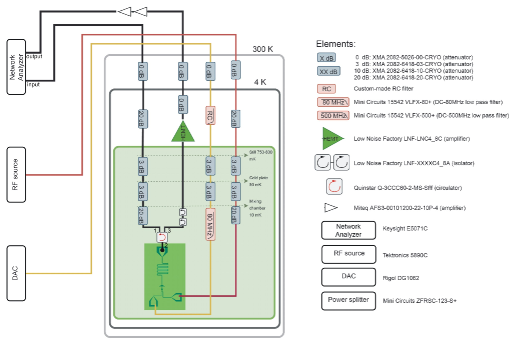
The measurement scheme exploited in this work is illustrated in Fig. S2. The sample is mounted in a aluminum box and thermally anchored to a dilution refrigerator with a base temperature of 10 mK. The readout cavity of device is connected to the input and output of a network analyzer for scattering parameters (S21) measurement. A Digital-to-Analog Converter (DAC) used for applying DC voltage is connected to the Z-control line for magnetic flux tuning, while a RF source used for applying additional tone for two-tone measurements is connected to the XY-control line [Fig. S2]. More details of the measurement scheme and the associated components can be found in section II in the supplementary material.
III III. Device characterization and results
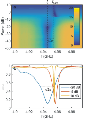
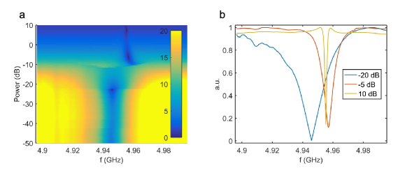
The SQUID along with the shunting capacitor is coupled to a /2 superconducting reflective cavity with a bare resonant frequency 4.955 GHz and a loaded quality factor Q 3964 obtained / from the trace of P = 10 dB in Fig. 2(b). We first performed a standard qubit power-dependent experiment, in which the S21 is measured as a function of the input power applied to the readout line, as shown in Fig. 2(a). This is a conventional way to confirm the existence of JJ in transmonReed et al. (2010), where the resonant frequency of the cavity shifts toward the transmon frequency at large enough power (here at around -5 dB). Here, we note that we have not demonstrated temporal coherence or energy-level spectroscopy in our device, which does not justify the device as a transmon. However, for simplicity we still use terms, such as transmon frequency or transmon-cavity coupling, in the following content. The power-dependent frequency shift is generally attributed to the nonlinearity that cavity inherits from JJs, in which cavity can not be approximated to a perfect harmonic oscillator as the photon occupation number increases Reed et al. (2010). Fig. 2(b) shows the linecuts at different powers. At lower power (-20 dB), the cavity frequency centers at 4.945 GHz with an asymmetric line shape, indicating a canonical behavior of a Kerr-Duffing oscillator Reed (2014). The peak exists until P -10 dB, beyond which the cavity response undergoes a broad regime (see section III in the supplementary material). Beyond a critical power (P -5 dB), the cavity response re-appears, with a narrower line shape of Lorentzian and a frequency shifted to 4.957 GHz, as shown in Fig. 2(b). As the power further increases, the cavity linewidth continue to decrease, which is expected for a MoRe cavity in an elevated power Singh et al. (2020). However, while the power is increased, surprisingly the peak position still moves slightly with power, eventually reaching a stable value of around 4.955 GHz at P = 10 dB. This is known as the bare cavity frequency at which the cavity would resonate in the absence of transmon’s JJs. This effect is more pronounced in Fig. S3, where we have reduced the attenuation on the readout-in line to apply larger powers. The reason for the post-bright-regime frequency shift is not fully decisive. We suspect it could be due to the residual nonlinearity (in the range of -5 dB P 10 dB) that cavity still inherited from one junction, while the other one was saturated earlier at a relatively lower power.
The magnitude of the shift between cavity’s frequency at low power () and at high-power (), as shown in Fig. 2(a), allows us to estimate the transmon frequency via , where is the transmon-cavity coupling strength and is the difference between and the transmon frequency . In our system, is estimated to be 116 MHz (see section IV in the supplementary material), from which we can infer 6.29 GHz. The fact that 1 indicates our transmon is working in the dispersive regime. However, is close to the cavity decay rate [see Fig. 2(b)], which does not satisfy the strong dispersive condition of and may in fact place a limitation for us to perform the state-dependent readout of cavity. The relaxation time T1 set by Purcell effect can be expressed as , where is the rate at which the transmon decays due to the Purcell effect Koch et al. (2007); Houck et al. (2008). Substituting 20 MHz, 116 MHz and = = 6.29 4.945 = 1.345 GHz, we estimate an upper bound of 1 s. In an attempt to measure the relaxation time, we have performed the two-tone measurement, in which an additional drive tone searching for transmon frequency is applied to the XY-control line (see section V in the supplementary materials). However, no state-dependent cavity response was observed, indicating a very short coherence time. In future endeavor, we anticipate an improved Q-factor in readout cavity could suppress the Purcell decay and thus enhance . In addition, by replacing SiO2 dielectric layer, careful transfer of 2D materials to form cleaner JJ interfaces, and increased magnetic and infrared radiation shielding, and are expected to be further improved Oliver and Welander (2013); O’Connell et al. (2008); Córcoles et al. (2011); Barends et al. (2011); Place (2020). Transmon frequency is the transition frequency from the ground state to the first excited state of the transmon and can be expressed as = , where = is the charging energy and = is the Josephson energy ( = is the flux quantum). From electrostatic simulations we estimate a charging energy of 222 MHz ( 87 fF, see section IV in the supplementary material). Combined with = 6.29 GHz, we can infer the Josephson energy 22 GHz and the critical current of the SQUID 44.2 nA. By changing the magnetic flux threading the loop of SQUID, we are able to change the critical current, hence and , which leads to different to be measured. The flux-tunability of cavity frequency allows us to distinguish the SQUID operation regime from the cavity bright state. Fig. 3 shows the resonant frequency of cavity as a function of flux bias at different readout-in powers. At lower power (P = -22 dB), cavity peak shows a periodic modulation with magnetic flux, while at higher powers (P = -3 dB and 10 dB), cavity frequency presents no flux modulation as JJs acting as absent due to entering the bright regime.
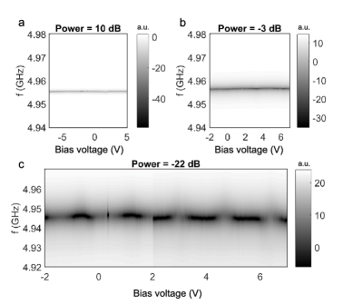
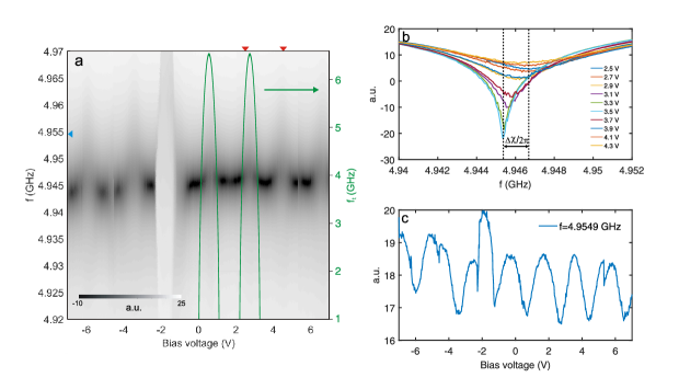
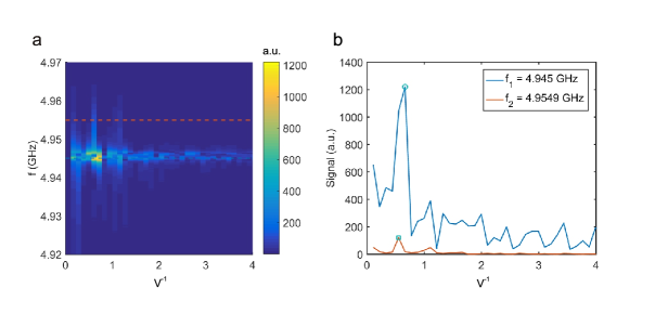
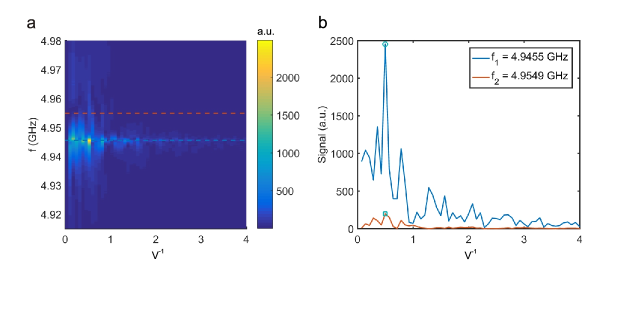
We further investigate the flux-tunability of the SQUID in more details as shown in Fig. 4(a), where cavity’s resonant frequency is measured as a function of bias voltage applied to the Z-control line at P = -20 dB. The cavity frequency shows a periodic oscillation with bias voltage, resembling the behavior of conventional transmon made of Al/Al2O3-based SQUID Chow (2010). Note that there is a vertical stripe mode at Vb -1.8 V, which is of unknown origin and not periodic in flux thus not related to the SQUID. It could be due to an accidentally formed magnetic impurity or field-tunable two-level system with energy coincides with cavity frequency at that bias voltage. Fig. 4(b) show the linecuts along the frequency axis in Fig. 4(a), with Vb varied between Vb = 2.5 V and 4.3 V in an equal step of 0.2 V [range marked by red triangles in Fig. 4(a)]. In this bias range, the peak position moves away and restores, which corresponds one period of flux tuning and allows us to obtain the maximal tunability 1.5 MHz. Using , with the lowest 8.5 MHz and the highest 4.9465 GHz, we can extract the maximum transmon frequency 6.53 GHz. The transmon frequency based on a symmetric SQUID oscillates against flux and can be approximated as , where = is the flux quantum and is the magnetic flux threading the loop of SQUID Krantz et al. (2020). Thus, the transmon frequency can be inferred as shown in green solid lines in Fig. 4(a). In Fig. 4(c), we show the linecut along the bias direction at a frequency of 4.9549 GHz [see the blue triangle in Fig. 4(a)], in order to obtain more insights on the flux tuning. In a topological material with helical electronic states, the supercurrent flowing in its Josephson junction can be a combination of both 4- and 2-periodic phase term Li et al. (2018); Wang et al. (2018); Badiane et al. (2013), namely = [+], where the index 1(2) denotes junction 1 (2) in the SQUID, and represent the 4 and 2 components of the supercurrent, and and are the weight of each component in a junction. Note that is the phase across junction 1(2) in the SQUID and has the relation of = + 2. Since the supercurrent through SQUID is a sum of and , it has the form of = + + + . Here, denote the the weight of 4 (2) supercurrent component in junction 1, while denote the the weight of 4 (2) supercurrent component in junction 2, respectively. Because the weight of 4 and 2 component in each junction is unknown, , , and are undetermined parameters. Considering the terms associated with , the overall supercurrent is single-period in flux tuning if one of the components (i.e., either or ) dominates the supercurrent. However, if the weight of 2 and 4 component is similar (i.e., ), the supercurrent can exist a flux oscillation with unequal spacing between neighboring peaks. This single-period and non-single-period behavior in supercurrent should also reflect on the flux modulation of cavity frequency. In order to gain more insight on the periodicity, we have performed Fourier transform (FT) on the 2D diagram of Fig. 4(a) and the trace shown in Fig. 4(c), and the results are shown in Fig. 5(a) and Fig. 5(b), respectively. Note we also performed FT on the data shown in Fig. 3(c) for comparison, as presented in section VI in the supplementary material. The 2D map of FT in Fig. 5(a) and the linecuts at both f = 4.9455 GHz and f = 4.9549 GHz in Fig. 5(b) indeed show a dominant spectral component at around 0.5 V-1, which corresponds to the oscillation period V 2V in Fig. 4(c). The FT signals in Fig. 5(a) show some level of broadness around 0.5 V-1, possibly due to the glitch noises in Fig. 4(a) [i.e., around bias voltage -4.5 V and 5.5 V]. In a topological junction, the 2-periodic supercurrent (bulk transport) is expected to inevitably contribute to the overall supercurrent, while the 4 supercurrent often requires careful tuning to appear Wang et al. (2018); Li et al. (2018). It is also worth noting that the 4-periodic supercurrent tends to restore 2 periodicity, as a result of various relaxation processes Kwon et al. (2004); San-Jose et al. (2012); Rainis and Loss (2012). These relaxation mechanisms should play a role in DC measurements, and are in fact the reason that RF SQUIDs were adopted to probe the existence of 4-periodic supercurrent in topological junctions Bocquillon et al. (2017); Li et al. (2018). Although our measurement is based on microwave techniques operating at GHz, the integrated measurement time is around seconds, which may still suffer from the relaxation processes happening at a time scale around microseconds Badiane et al. (2013); Rainis and Loss (2012). Thus, we attribute the component at around 0.5 V-1 to the 2-periodic supercurrent. On the other hand, we do not see an evident FT signal at around 0.25 V-1 which corresponds to 4-periodic supercurrent (see also section VI for similar analysis on the FT of Fig. 3(c)). In future endeavor, a device with gates to tune between trivial bulk state and topological surface state Wang et al. (2018), which allows one to switch supercurrent between 2- and 4-period, would help to understand whether these relaxation processes play a role in this type of measurement.
IV IV. Summary
In summary, we have fabricated and characterized a transmon-like superconducting quantum circuit made of Weyl semimetal MoTe2 and superconducting cavity of MoRe. The successfully made MoTe2 Josephson junction revealed itself in the qubit power-dependent measurement. The power-dependent cavity frequency shift allows us to extract the transmon frequency, Josephson energy and the critical current flowing through the SQUID. The cavity frequency is tunable with magnetic flux applied to the loop of SQUID area, indicating the flux modulation of transmon frequency. The flux-tuning shows a single-period oscillation, suggesting the 2-phase term is the dominating contribution in the supercurrent or the measurement is mediated by the relaxation processes which tend to restore the 4 to 2 periodicity in a topological junction. Our study demonstrates a flux-tunable SQUID quantum circuit based on topological material. The transmon-like geometry provide a platform for use in quantum information processing in the future.
V V. Acknowledgments
K. L. Chiu would like to acknowledge Karl Petersson, Tongxing Yan, Peng Duan, Fei Yan and Siyuan Han for the useful discussions on data analysis. The authors would like to thank the funding support from Guangdong Provincial Key Laboratory (Grant No. 2019B121203002), National Natural Science Foundation of China (Grant No. 11934010) and Ministry of Science and Technology of Taiwan (Grant No. MOST 109-2112-M-110-005-MY3).
VI VI. Author contributions
K.L.C conceived the project. D.G.Q fabricated the devices with contributions from K.L.C, Z.T.Z, S.L, Y.Z and D.P.Y. K.L.C performed the measurements with contributions from J.W.C and W.Y.L. K.L.C, V.M and D.T analyzed the data. K.L.C wrote the manuscript with input from all the co-authors.
VII VII. Declaration
The order of affiliation does not represent the contributing order, Shenzhen Institute for Quantum Science and Engineering and National Sun Yat-Sen University are the co-first institute in this work. Device fabrications and measurements were performed in Shenzhen Institute for Quantum Science and Engineering, while data process and analysis were carried out in National Sun Yat-Sen University.
References
- Armitage et al. (2018) N. P. Armitage, E. J. Mele, and A. Vishwanath, Weyl and Dirac semimetals in three-dimensional solids, Rev. Mod. Phys. 90, 015001 (2018), URL https://link.aps.org/doi/10.1103/RevModPhys.90.015001.
- Soluyanov et al. (2015) A. A. Soluyanov, D. Gresch, Z. Wang, Q. Wu, M. Troyer, X. Dai, and B. A. Bernevig, Type-II Weyl semimetals, Nature 527, 495 (2015), URL http://dx.doi.org/10.1038/nature15768.
- Chang et al. (2016) T.-R. Chang, S.-Y. Xu, G. Chang, C.-C. Lee, S.-M. Huang, B. Wang, G. Bian, H. Zheng, D. S. Sanchez, I. Belopolski, et al., Prediction of an arc-tunable Weyl Fermion metallic state in MoxW1-xTe2, Nature Communications 7, 10639 (2016), URL http://dx.doi.org/10.1038/ncomms10639.
- Jiang et al. (2017) J. Jiang, Z. Liu, Y. Sun, H. Yang, C. Rajamathi, Y. Qi, L. Yang, C. Chen, H. Peng, C.-C. Hwang, et al., Signature of type-II Weyl semimetal phase in MoTe2, Nature Communications 8, 13973 (2017), URL http://dx.doi.org/10.1038/ncomms13973.
- Li et al. (2017) P. Li, Y. Wen, X. He, Q. Zhang, C. Xia, Z.-M. Yu, S. A. Yang, Z. Zhu, H. N. Alshareef, and X.-X. Zhang, Evidence for topological type-II Weyl semimetal WTe2, Nature Communications 8, 2150 (2017), URL https://doi.org/10.1038/s41467-017-02237-1.
- Shvetsov et al. (2018) O. O. Shvetsov, A. Kononov, A. V. Timonina, N. N. Kolesnikov, and E. V. Deviatov, Realization of a double-slit SQUID geometry by Fermi arc surface states in a WTe2 Weyl semimetal, JETP Letters 107, 774 (2018), URL https://doi.org/10.7868/S0370274X18120081.
- Wang et al. (2018) A.-Q. Wang, C.-Z. Li, C. Li, Z.-M. Liao, A. Brinkman, and D.-P. Yu, 4-Periodic Supercurrent from Surface States in Cd3As2 Nanowire-Based Josephson Junctions, PRL 121, 237701 (2018), URL https://link.aps.org/doi/10.1103/PhysRevLett.121.237701.
- Casparis et al. (2018) L. Casparis, M. R. Connolly, M. Kjaergaard, N. J. Pearson, A. Kringhøj, T. W. Larsen, F. Kuemmeth, T. Wang, C. Thomas, S. Gronin, et al., Superconducting gatemon qubit based on a proximitized two-dimensional electron gas, Nature Nanotechnology 13, 915 (2018), ISSN 1748-3395, URL https://doi.org/10.1038/s41565-018-0207-y.
- Chiu (2018) K. L. Chiu, Single electron transport and possible quantum computing in 2D materials, arXiv e-prints arXiv:1804.02870 (2018).
- Kroll et al. (2018) J. G. Kroll, W. Uilhoorn, K. L. van der Enden, D. de Jong, K. Watanabe, T. Taniguchi, S. Goswami, M. C. Cassidy, and L. P. Kouwenhoven, Magnetic field compatible circuit quantum electrodynamics with graphene Josephson junctions, Nature Communications 9, 4615 (2018), ISSN 2041-1723, URL https://doi.org/10.1038/s41467-018-07124-x.
- Wang et al. (2019) J. I.-J. Wang, D. Rodan-Legrain, L. Bretheau, D. L. Campbell, B. Kannan, D. Kim, M. Kjaergaard, P. Krantz, G. O. Samach, F. Yan, et al., Coherent control of a hybrid superconducting circuit made with graphene-based van der Waals heterostructures, Nature Nanotechnology 14, 120 (2019), ISSN 1748-3395, URL https://doi.org/10.1038/s41565-018-0329-2.
- Chiu and Xu (2017) K.-L. Chiu and Y. Xu, Single-electron Transport in Graphene-like Nanostructures, Physics Reports 669, 1-42 (2017), URL https://doi.org/10.1016/j.physrep.2016.12.002.
- Chien et al. (2020) Wei-Chen Chien, Shun-Jhou Jhan, Kuei-Lin Chiu, Yu-xi Liu, Eric Kao, and Ching-Ray Chang, Cryogenic Materials and Circuit Integration for Quantum Computers, Journal of Electronic Materials 49, 6844–6858 (2020), URL https://doi.org/10.1007/s11664-020-08442-x.
- Schmitt (2020) Tobias W. Schmitt, Malcolm R. Connolly, Michael Schleenvoigt, Chenlu Liu, Oscar Kennedy, Abdur R. Jalil, Benjamin Bennemann, Stefan Trellenkamp, Florian Lentz, Elmar Neumann, Tobias Lindström, Sebastian E. de Graaf, Erwin Berenschot, Niels Tas, Gregor Mussler, Karl D. Petersson, Detlev Grützmacher and Peter Schüffelgen, Integration of selectively grown topological insulator nanoribbons in superconducting quantum circuits, arXiv e-prints arXiv:2007.04224 (2020).
- Fu and Kane (2009) L. Fu and C. L. Kane, Josephson current and noise at a superconductor/quantum-spin-Hall-insulator/superconductor junction, Phys. Rev. B 79, 161408 (2009), URL https://link.aps.org/doi/10.1103/PhysRevB.79.161408.
- Fu and Kane (2008) L. Fu and C. L. Kane, Superconducting Proximity Effect and Majorana Fermions at the Surface of a Topological Insulator, Phys. Rev. Lett. 100, 096407 (2008), URL http://link.aps.org/doi/10.1103/PhysRevLett.100.096407.
- Badiane et al. (2013) D. M. Badiane, L. I. Glazman, M. Houzet, and J. S. Meyer, Ac Josephson effect in topological Josephson junctions, Comptes Rendus Physique 14, 840 (2013), ISSN 1631-0705, URL http://www.sciencedirect.com/science/article/pii/S1631070513001692.
- R. et al. (2010) C. R. Dean, A. F. Young, I. Meric, C. Lee, L. Wang, S. Sorgenfrei, K. Watanabe, T. Taniguchi, P. Kim, K. L. Shepard, et al., Boron nitride substrates for high-quality graphene electronics, Nature Nanotechnology 5, 722 (2010), ISSN 1748-3387, URL http://dx.doi.org/10.1038/nnano.2010.172.
- Mayorov et al. (2011) A. S. Mayorov, R. V. Gorbachev, S. V. Morozov, L. Britnell, R. Jalil, L. A. Ponomarenko, P. Blake, K. S. Novoselov, K. Watanabe, T. Taniguchi, Micrometer-Scale Ballistic Transport in Encapsulated Graphene at Room Temperature, et al., Nano Lett. 11, 2396 (2011), ISSN 1530-6984, URL http://dx.doi.org/10.1021/nl200758b.
- Haigh et al. (2012) S. J. Haigh, A. Gholinia, R. Jalil, S. Romani, L. Britnell, D. C. Elias, K. S. Novoselov, L. A. Ponomarenko, A. K. Geim, and R. Gorbachev, Cross-sectional imaging of individual layers and buried interfaces of graphene-based heterostructures and superlattices, Nature Materials 11, 764 (2012), ISSN 1476-1122, URL http://dx.doi.org/10.1038/nmat3386.
- Wang et al. (2013) L. Wang, I. Meric, P. Y. Huang, Q. Gao, Y. Gao, H. Tran, T. Taniguchi, K. Watanabe, L. M. Campos, D. A. Muller, et al., One-Dimensional Electrical Contact to a Two-Dimensional Material, Science 342, 614 (2013), URL http://www.sciencemag.org/content/342/6158/614.abstract.
- Reed et al. (2010) M. D. Reed, L. DiCarlo, B. R. Johnson, L. Sun, D. I. Schuster, L. Frunzio, and R. J. Schoelkopf, High-Fidelity Readout in Circuit Quantum Electrodynamics Using the Jaynes-Cummings Nonlinearity, PRL 105, 173601 (2010), URL https://link.aps.org/doi/10.1103/PhysRevLett.105.173601.
- Reed (2014) M. D. Reed, High-Fidelity Readout in Circuit Quantum Electrodynamics Using the Jaynes-Cummings Nonlinearity, Ph.D. thesis, Yale University (2014).
- Singh et al. (2020) V. Singh, B. H. Schneider, S. J. Bosman, E. P. J. Merkx, and G. A. Steele, Molybdenum-rhenium alloy based high-Q superconducting microwave resonators, Appl. Phys. Lett. 105, 222601 (2014), ISSN 0003-6951, URL https://doi.org/10.1063/1.4903042.
- Koch et al. (2007) J. Koch, T. M. Yu, J. Gambetta, A. A. Houck, D. I. Schuster, J. Majer, A. Blais, M. H. Devoret, S. M. Girvin, and R. J. Schoelkopf, Charge-insensitive qubit design derived from the Cooper pair box, Phys. Rev. A 76, 042319 (2007), URL https://link.aps.org/doi/10.1103/PhysRevA.76.042319.
- Houck et al. (2008) A. A. Houck, J. A. Schreier, B. R. Johnson, J. M. Chow, J. Koch, J. M. Gambetta, D. I. Schuster, L. Frunzio, M. H. Devoret, S. M. Girvin, et al., Controlling the Spontaneous Emission of a Superconducting Transmon Qubit, Phys. Rev. Lett. 101, 080502 (2008), URL https://link.aps.org/doi/10.1103/PhysRevLett.101.080502.
- Oliver and Welander (2013) W. D. Oliver and P. B. Welander, Materials in superconducting quantum bits, MRS Bulletin 38, 816 (2013), ISSN 0883-7694, URL https://www.cambridge.org/core/article/materials-in-superconducting-quantum-bits/B7A4DC8B7F54A0715CEFAFE6677F33D8.
- O’Connell et al. (2008) A. D. O’Connell, M. Ansmann, R. C. Bialczak, M. Hofheinz, N. Katz, E. Lucero, C. McKenney, M. Neeley, H. Wang, E. M. Weig, et al., Microwave dielectric loss at single photon energies and millikelvin temperatures, Appl. Phys. Lett. 92, 112903 (2008), ISSN 0003-6951, URL https://doi.org/10.1063/1.2898887.
- Córcoles et al. (2011) A. D. Córcoles, J. M. Chow, J. M. Gambetta, C. Rigetti, J. R. Rozen, G. A. Keefe, M. Beth Rothwell, M. B. Ketchen, and M. Steffen, Protecting superconducting qubits from radiation, Appl. Phys. Lett. 99, 181906 (2011), ISSN 0003-6951, URL https://doi.org/10.1063/1.3658630.
- Barends et al. (2011) R. Barends, J. Wenner, M. Lenander, Y. Chen, R. C. Bialczak, J. Kelly, E. Lucero, P. O’Malley, M. Mariantoni, D. Sank, et al., Minimizing quasiparticle generation from stray infrared light in superconducting quantum circuits, Appl. Phys. Lett. 99, 113507 (2011), ISSN 0003-6951, URL https://doi.org/10.1063/1.3638063.
- Place (2020) Alex P. M. Place, Lila V. H. Rodgers, Pranav Mundada, Basil M. Smitham, Mattias Fitzpatrick, Zhaoqi Leng, Anjali Premkumar, Jacob Bryon, Sara Sussman, Guangming Cheng, Trisha Madhavan, Harshvardhan K. Babla, Berthold Jaeck, Andras Gyenis, Nan Yao, Robert J. Cava, Nathalie P. de Leon, Andrew A. Houck, et al., New material platform for superconducting transmon qubits with coherence times exceeding 0.3 milliseconds, arXiv e-prints arXiv:2003.00024 (2020).
- Chow (2010) J. M. Chow, Quantum Information Processing with Superconducting Qubits, Ph.D. thesis, Yale University (2010).
- Krantz et al. (2020) P. Krantz, M. Kjaergaard, F. Yan, T. P. Orlando, S. Gustavsson, and W. D. Oliver, A quantum engineer’s guide to superconducting qubits, Applied Physics Reviews 6, 021318 (2020), URL https://doi.org/10.1063/1.5089550.
- Li et al. (2018) C. Li, J. C. de Boer, B. de Ronde, S. V. Ramankutty, E. van Heumen, Y. Huang, A. de Visser, A. A. Golubov, M. S. Golden, and A. Brinkman, 4-periodic Andreev bound states in a Dirac semimetal, Nature Materials 17, 875 (2018), ISSN 1476-4660, URL https://doi.org/10.1038/s41563-018-0158-6.
- Kwon et al. (2004) H.-J. Kwon, K. Sengupta, and V. M. Yakovenko, Fractional ac Josephson effect in p- and d-wave superconductors, The European Physical Journal B - Condensed Matter and Complex Systems 37, 349 (2004), ISSN 1434-6036, URL https://doi.org/10.1140/epjb/e2004-00066-4.
- San-Jose et al. (2012) P. San-Jose, E. Prada, and R. Aguado, Ac Josephson Effect in Finite-Length Nanowire Junctions with Majorana Modes, Phys. Rev. Lett. 108, 257001 (2012), URL https://link.aps.org/doi/10.1103/PhysRevLett.108.257001.
- Rainis and Loss (2012) D. Rainis and D. Loss, Majorana qubit decoherence by quasiparticle poisoning, Phys. Rev. B 85, 174533 (2012), URL https://link.aps.org/doi/10.1103/PhysRevB.85.174533.
- Bocquillon et al. (2017) E. Bocquillon, R. S. Deacon, J. Wiedenmann, P. Leubner, T. M. Klapwijk, C. Brüne, K. Ishibashi, H. Buhmann, and L. W. Molenkamp, Gapless Andreev bound states in the quantum spin Hall insulator HgTe, Nature Nanotechnology 12, 137 (2017), ISSN 1748-3395, URL https://doi.org/10.1038/nnano.2016.159.
- Bishop et al. (2010) L. S. Bishop, E. Ginossar, and S. M. Girvin, Response of the Strongly Driven Jaynes-Cummings Oscillator, Phys. Rev. Lett. 105, 100505 (2010), URL https://link.aps.org/doi/10.1103/PhysRevLett.105.100505.
- Larsen et al. (2015) T. W. Larsen, K. D. Petersson, F. Kuemmeth, T. S. Jespersen, P. Krogstrup, J. Nygård, and C. M. Marcus, Semiconductor-Nanowire-Based Superconducting Qubit, Phys. Rev. Lett. 115, 127001 (2015), URL https://link.aps.org/doi/10.1103/PhysRevLett.115.127001.
- Schuster et al. (2005) D. I. Schuster, A. Wallraff, A. Blais, L. Frunzio, R.-S. Huang, J. Majer, S. M. Girvin, and R. J. Schoelkopf, ac Stark Shift and Dephasing of a Superconducting Qubit Strongly Coupled to a Cavity Field, Phys. Rev. Lett. 94, 123602 (2005), URL https://doi.org/10.1103/PhysRevLett.94.123602.
Supplementary materials
I I. Device fabrication
The general steps for device fabrication has been specified in the main text. Here, we provide more details during different stages in fabrication. After the sputtering of 80 nm MoRe (Ar flow: 50 sccm, Pressure: 0.57 Pa, Rate: 3.3 A/s) onto the intrinsic Si wafers capped with 285 nm SiO2, the structures of cavity and feedlines are defined by a laser writer (Resist: S1813, Developer: MIF 319). After the ICP etching (SF6: 40 sccm, Ar: 10 sccm), the optical micrograph of the as-made cavity and control lines is shown in Fig. S1(a). Afterwords, a strip of multilayered MoTe2 was transferred onto the square area, as shown in Fig. S1(b), using a dry-polymer based process Wang et al. (2013). Note that all the exfoliation and transfers were performed in a N2 filled glove box to prevent the air-sensitive Td-MoTe2 from degradation. The device was immediately covered by PMMA after the completion of transfer. After a writing of electron-beam lithography and sputtering of superconducting leads (NbN), the SQUID is fabricated as shown in Fig. S1(c). Note that we do not do the ion mill between the superconducting leads and cavity, because the oxidation of MoRe is negligible during our fabrication processes.
II II. Measurement scheme
Fig. S2 shows the measurement scheme used in this work. All the experiments detailed in the main text were performed in a dilution refrigerator with a base temperature of 10 mK. The devices were bonded in a light tight Al box which is thermally anchored to the mixing chamber and enclosed in a Al cylinder shield to prevent flux noises. The scheme showns in Fig. S2 is adopted to perform the power-dependence and flux-tuning of cavity’s resonant frequency. In this setup, four coaxial lines were used to control the device: two are assigned for cavity readout, one for flux control and one for drive tone. The cavity readout line represented by black solid line in Fig. S2 consists of an input and an output line, as shorted by readout-in and readout-out in the following content. The readout-in line connected to the input of a network analyzer (Keysight E5071C) is heavily attenuated in low temperature to reduce noise and thermal excitation before connecting to a circulator (port 1). The second port of the circulator is connected to the reflective cavity of device. The reflected readout signal is out through the third port of circulator and goes into the readout-out line. The readout-out line was connected to two isolators in series to shield the device from thermal radiation from the HEMT amplifier on the 4K stage. The HEMT (LNF-LNC4 8C) has about 40 dB of gain and a noise temperature of 2 K. The readout signal is further amplified by two room-temperature amplifiers before going into the output of the network analyzer. The flux-tuning line represented by yellow solid line in Fig. S2 was connected to a DAC (Rigol DG 1062) to apply DC voltage. This line is heavily filtered by a home-made RC filter at 4 K and a 80 MHz low-passed filter at 10 mK to reduce the thermal noises of frequencies greater than 300 kHz. The applied DC voltage to the 1.5 k resistor in the RC filter allows us to generate a DC current in device’s Z-control line for flux tuning. The drive-tone line was connected to a RF source (Tektronic 5890c) in room temperature and heavily attenuated in low temperature, again to reduce the unwanted noises, as shown in the red solid line in Fig. S2.
III III. Power dependence
For a conventional transmon qubit, Bishop developed a semiclassical model under the bad cavity and strong-dispersive approximations Bishop et al. (2010):
| (S1) |
where is the cavity dispersive shift, is cavity amplitude (drive amplitude), is the cavity-qubit detuning, is the coupling strength between the cavity and qubit, and is Pauli matrix. This equation satisfies the relations and = 0, meaning the anharmonicity of the cavity (e.g. the difference in for and excitations) is maximal at low power and continuously diminish as the drive strength is increased. In a conventional transmon qubit Reed et al. (2010), the cavity response is linear at the zero-power limit, but as the drive strength increases, the turn-on of anharmonicity would distort the line shape and result in dips, which Bishop attributes to the ensemble-averaging of the bistalbe solutions of amplitude in Eq. S1 Bishop et al. (2010). In our case, we attribute the broad regime, i.e. -15 dB P -10 dB in Fig. S3 (a), to the destructive interference of the two semiclassical solutions of with almost opposite phases. Finally, with the drive strength further increases, the frequency extent of the bistable region shrinks and eventually cavity shift into resonance with the drive. At this point, the cavity population rapidly grow while its anharmonicity shrinks – thus reaching the bright state.
IV IV. coupling strength estimation
Fig. S4 shows the effective circuit diagram of our transmon-like SQUID device. The two Josephson junctions are shunted by the capacitance between the T-shape island and ground. is the capacitance between the readout cavity and T-shape island while () is the effective capacitance (inductance) of the readout cavity, where is the cavity resonant frequency. Substituting = 50, = 1 and = 2 4.955 GHz, we get = 1 pF, which is close to the simulated value 1.4 pF [leftmost panel in Fig. S4 (b)]. For other parameters, we use Sonnet Software to simulate the capacitance to get = 5 fF and = 82 fF, as shown in Fig. S4 (b). The qubit-cavity coupling strength can be expressed as = , where = Koch et al. (2007). Substituting all the parameters we have = 116 MHz, which is in agreement with the value in a similar design in Ref. Larsen et al. (2015).
V V. Two-tone measurements
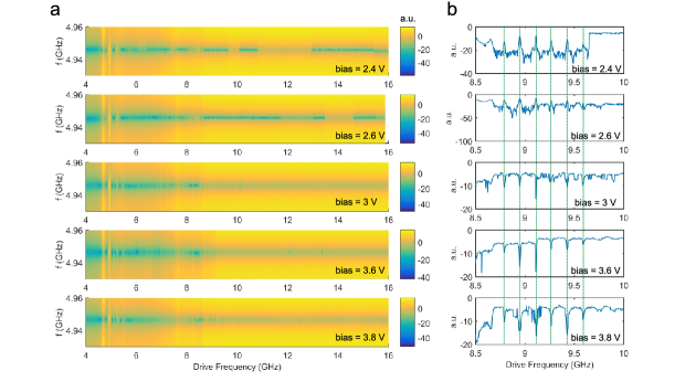
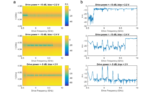
Two-tone spectroscopy was performed by measuring S21 as a function of frequency of a tone applied to the readout cavity and another tone applied to the XY-control line. Our result is shown in Fig. S5(a), in which the y-axis is the readout frequency measured by network analyzer while the x-axis is the drive frequency generated by a RF source. We have performed this measurement at different applied biases ranging from 2.4 V to 3.8 V. However, no shift in cavity frequency was observed in the whole probed range of drive frequency, indicating a very short coherence time. As seen in Fig. 4(a), the fact that the transmon frequency crosses the cavity periodically but does not form avoided crossings, indicates the device is not in the strong coupling regime (i.e., , , where is the transmon-cavity energy exchange rate and () is transmon (cavity) decay rate). In this case, our transmon should have a decay rate = = 232 MHz, hence a coherence time 1/ 4.3 ns. In the experiment of energy level spectroscopy, the linewidth of the spectroscopic peak is = Schmitt (2020); Schuster et al. (2005). Thus, for a device with coherence less than 4 ns, the linewidth would be at least greater than 80 MHz. One would expect to see only a very hazy spectroscopy line, since the integrated area of the resonance line is a fixed quantity, and if it is spread over more than 80 MHz, it’s value at the center frequency would be largely indistinguishable from the majority of the linewidth. In our measurements, we observed a periodic feature in the lincuts at cavity resonant frequency and in the range between 8.5 GHz and 10 GHz in drive frequency [Fig. S5(b)]. These oscillating peaks appear at all bias voltages and their position is independent of the applied biases (i.e., transmon frequencies), as indicated by the green dashed lines in Fig. S5(b). In addition, the resonances were only observable at very high power, as shown in Fig. S6. These oscillations may be associated with a standing wave (f 159 MHz, 1.25 m) in the coaxial cables, as also being reported in Ref. Kroll et al. (2018).
VI VI. Flux periodicity analysis
The Fourier transform (FT) of Fig. 3(c) is shown in Fig. S7. The dominant spectral component at around 0.5 V-1 is also observed, which is consistent with the observations in Fig. 5. However, there appears to be a non-ignorable component around 1.1 V-1, which survives even at higher frequencies. In our topological junctions, we anticipate the 2-periodic supercurrent is an inevitable contribution and should correspond to the 0.5 V-1 in both Fig. 5 and Fig. S7. As depicted in the main text, the 2-periodic supercurrent has the flux relation of , while the 4-periodic supercurrent has that of . If the FT component at 0.5 V-1 corresponds to the 2 supercurrent, the 4 supercurrent should appear at around 0.25 V-1, not 1.1 V-1. Therefore, we conclude that the signal at 1.1 V-1 in Fig. S7 does not represent the 4-periodic supercurrent. On the contrary, if the FT signal at 0.5 V-1 in both Fig. 5 and Fig. S7 corresponds to the 4 supercurrent, there should be a signal at around 1 V-1 corresponding to 2 supercurrent, but it is not observed in Fig. 5.