MoS2 and Janus (MoSSe) Based 2D van der Waals Heterostructures: Emerging Direct Z-scheme Photocatalysts†
Abstract
Two-dimensional (2D) materials viz. transition metal dichalcogenides (TMD) and transition metal oxides (TMO) offer a platform that allows creation of heterostructures with a variety of properties. The optoelectronic industry has observed an upheaval in the research arena of MoS2 based van der Waals (vdW) heterostructures (HTSs) and Janus structures. Therefore, interest towards these structures are backed by the selectivity in terms of electronic and optical properties. The present study investigates the photocatalytic ability of bilayer, MoS2 and Janus (MoSSe) based vdW HTSs viz. MoS2/TMO, MoS2/TMD, MoSSe/TMO and MoSSe/TMD, by first-principles based approach under the framework of (hybrid) density functional theory (DFT) and many body perturbation theory (GW approximation). We have considered HfS2, ZrS2, TiS2, WS2 and HfO2, T-SnO2, T-PtO2 from the family of TMD and TMO, respectively. The photocatalytic properties of these vdW HTSs are thoroughly investigated and compared with the respective individual monolayers by visualizing their band edge alignment, electron-hole recombination and optical properties. Strikingly we observe that, despite most of the individual monolayers do not perform optimally as a photocatalyst, type II band edge alignment is noticed to vdW HTSs and they appear to be efficient for photocatalysis via Z-scheme. Moreover, these HTSs have also shown promising optical response in the visible region. Finally electron-hole recombination, H2O adsorption and hydrogen Evolution Reaction (HER) results establish that MoSSe/HfS2, MoSSe/TiS2, MoS2/T-SnO2, MoS2/ZrS2 and MoSSe/ZrS2 are probable, most efficient Z-scheme photocatalysts.
keywords:
DFT, Janus, Heterostrutcures, van der Waals, Z-scheme, Photocatalysis[subfigure]labelformat=parens,labelsep=space,font=small \phone+91-2659 1359 \fax+91-2658 2037
1 Introduction
In present context, solar energy is the supreme resource to combat energy and environment related issues. With an aim to enhance the utilization of solar energy, the field of photocatalysis for water splitting and pollutant degradation have gained interest 1, 2, 3, 4. Further, the demand for exciting materials that serve selectivity, have directed the focus towards the 2D materials. Amongst these, MoS2 is one of the widely studied 2D materials that belongs to the transition metal dichalcogenides (TMD) family. The other classification constitutes graphene family, transition metal oxides (TMOs) and MXenes 5. These materials have been vastly studied in the regimes of defect study 6, 7, photovoltaics 8, 9 and optoelectronics 10, 11. These widely studied (both theoretically and experimentally) TMDs are MoS2, MoSe2, WS2 and WSe2. However, other TMDs such as HfS2, ZrS2 and TiS2 have also been a matter of research for their salient electronic, vibrational and optical properties 12, 13, 14. Conversely, TMOs have not been established with similar level of experimental database as of TMDs. Lebègue et al. 15 indicate synthesis of TMOs as challenging due to the rare occurrence of their stable bulk phases. Only few of these materials have been synthesized experimentally 16. In this scenario, theoretical studies of the TMOs have showcased a huge potential, which helps in opening the scope of further research 17, 18. Another class of 2D materials that have recently drawn a lot of interest is Janus 19, 20. These materials, having the form of MXY (M = Mo and X,Y = O, S, Se and Te; XY), lack mirror symmetry and have vertical dipole 21, 22. It exhibits superior photocatalytic activities amongst its counterparts 23, 24. Engineering them for constructing van der Waals (vdW) heterostructures (HTSs) have established novel physics such as interlayer screening effects 25, 26, 27 and valley physics 28, 29, 30, etc. Therefore, the existing literatures indicate the aforementioned materials as promising in present research context 31, 32, 33, 34, 35, 36.
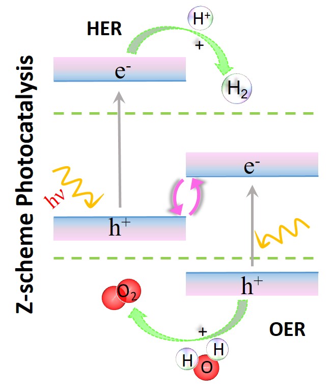
Here we intend to select the vdW HTSs for the study of photocatalytic water splitting. Now, the MoS2 monolayer with direct band gap and apt redox potentials is a good photocatalyst 37, 38. However, its performance is affected by the electron (e-) and hole (h+) recombination as the carriers are generated in the same spatial region 39. Therefore, an attempt in mitigating this issue is made by considering vdW HTSs, where due to the separation of e- - h+ carriers in different layer (i.e. different spatial region), they are considered to be a successful alternative for photocatalytic water splitting 40, 41. Here we have considered the class of vdW HTSs with type II band alignment for this application. Note that there are two types of photocatalysts in case of vdW HTSs (a) simple heterojunction photocatalysts and (b) Z-scheme systems. In former, Conduction Band Minimum (CBm) and Valence Band Maximum (VBM) of the vdW HTSs, straddle the redox potential 42, 43. Here CBm and VBM are on two different monolayers thereby facilitating spatial charge separation with reduction and oxidation reactions on different monolayer, respectively. But, to achieve sufficient redox ability for a specific reaction occurring on a single photocatalyst, a larger bandgap, that simultaneously inhibit e- - h+ recombination and correlates to higher oxidation/reduction ability, is required. However, to enhance the efficiency, a smaller bandgap is desirable to increase the efficiency of light harvesting. Therefore, it is of a paramount importance for improving the photocatalytic performance, where Z-scheme 44, 45, 46 brings the solution by manipulating the photogenerated e- - h+ pairs as shown in the Z-scheme mode (see Fig. 1). Like before, here as well having type II alignment is mandatory but the CBm and VBM of the vdW HTSs do not straddle the redox potentials in the same manner as before. The layer with CBm straddling the reduction level and the another layer with VBM straddling the oxidation level are involved in hydrogen evolution reaction (HER) and oxygen evolution reaction (OER), respectively (see Fig. 1). The higher interlayer recombination of e- - h+ as compared to that of intralayer is a necessary step in the process. Thus, photoabsorption is improved due to two different band gaps leading to HER and OER on different systems 47, 48, 49. The weak vdW interlayer interaction in vdW HTSs facilitates lubricancy or interlayer movement that further assists the Z-scheme photocatalysis 41. Although, some vdW HTSs have been studied under this regime 50, 41, 44, 51, no extensive study on MoS2 based vdW HTSs consisting of TMDs (viz. HfS2, ZrS2, TiS2) and TMOs (viz. HfO2, T-PtO2, T-SnO2) as second layer are observed so far. On a similar note, the database of Janus (MoSSe) based vdW HTSs for the photocatalytic application is at an initial stage 24, 20. Hence, there is a justified interest to explore their applicability as photocatalysts. The MoSSe based vdW HTSs have further given rise to two possible stacking arrangements. Contrary to the structure of MoS2, the MoSSe lacks mirror symmetry. Hence, it is crucial to compare the possible stacking configurations of MoSSe based vdW HTSs with the MoS2 based vdW HTSs, for the photocatalytic application.
In this article, we have presented an exhaustive comparative study of MoS2 and MoSSe based vdW HTSs, where the second layer is from the family of (i) TMDs viz. WS2, HfS2, ZrS2, TiS2 and (ii) TMOs viz. HfO2, T-PtO2, T-SnO2. The existing literatures so far, have not discussed the above listed vdW HTS configurations for the Z-scheme photocatalysis. Until date earlier reports exist only on monolayers of type II vdW HTSs of TMDs and TMOs for photocatalytic applications 52. Here, using state-of-the-art theoretical methodologies within the framework of hybrid density functional theory (DFT) and manybody perturbation theory (MBPT) (viz. G0W0) we have systematically studied the important parameters for photocatalytic applications. First, we introduce the different possible stable configurations of vdW HTSs. Next we discuss the band edge alignment of 2D monolayers and their corresponding vdW HTSs. Subsequently, their recombination path is well analyzed to check capability as a Z-scheme photocatalyst. Finally, their accurate optical response is computed and understood with MBPT technique for consideration in photocatalytic devices. Strikingly we observe that, despite most of the individual monolayers do not perform optimally as a photocatalyst, type II band edge alignment is noticed to vdW HTSs and they appear to be efficient for photocatalysis via Z-scheme.
2 Methodology
We have employed first-principles based methodology under the framework of DFT 53, 54, 55, 56, 57, 58. The PAW pseudopotentials are used in our calculations using plane wave basis set as employed in Vienna Ab initio Simulation Package (VASP) 59, 60, 61. The exchange-correlation (xc) interaction amongst electrons are accounted by Generalized Gradient Approximation (GGA) with the functional form as proposed by Perdew-Burke-Ernzerhof (PBE) 62, 63. The hybrid density functional has also been employed to account for the same with the functional proposed by Heyd-Scuseria-Ernzerhof (HSE06) 64. The hybrid functional (HSE06) considers 25% mixing of the short range Hartree-Fock (HF) exchange. Its long range part is described by GGA-PBE functional.
The vdW HTSs are optimized using PBE functional and HSE06 is used to determine single point energy. The conjugate gradient minimization is performed with the Brillouin Zone (BZ) sampling of K-grid and the energetics are obtained by the BZ sampling of K-grid. The energy tolerance of 0.001 meV and force tolerance of 0.001 eV/Å have been used for optimization. In the ground state calculations, the plane wave cut-off energy is set to 600 eV. The vdW HTSs are modelled with 20 Å vacuum in order to avoid electrostatic interactions between the periodic images. The two-body vdW interaction as devised by Tkatchenko-Scheffler has been employed 65, 66. The correction parameter is based on Hirshfeld partitioning of the electron density. Note that, we have not included spin-orbit coupling (SOC) in our calculations, since the previous literatures have reported only slight change in band gap due to the same 44, 67, 68. The optical properties are calculated using the GW approach 69, 70. We have performed hybrid calculations
(HSE06), as an initial step for single shot GW calculations [i.e. G0W0@HSE06].
3 Results and Discussions
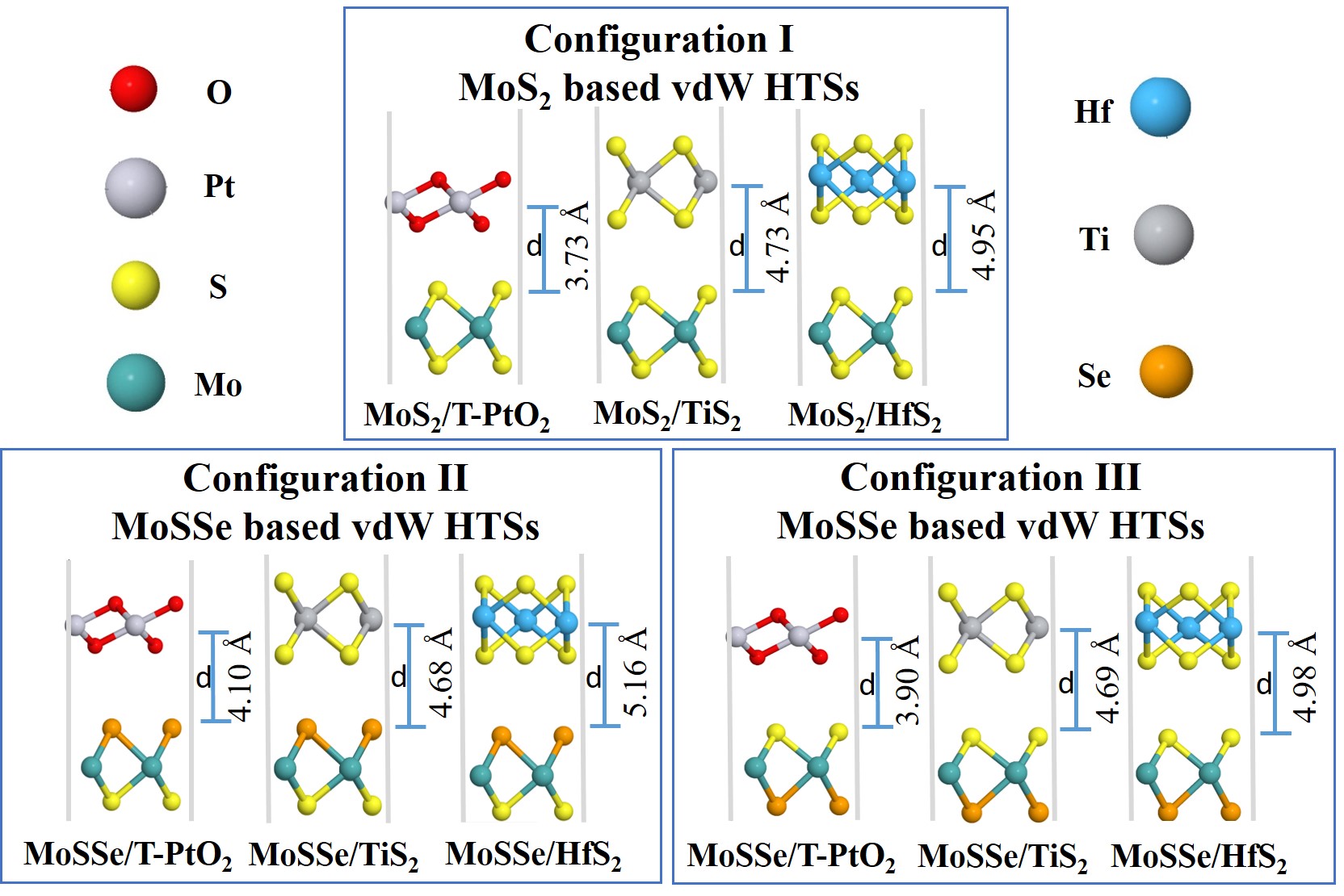
3.1 Heterostructure stacking
We have constructed commensurate bilayer vdW HTSs 71 with minimum lattice mismatch between the layers. The vdW HTSs have been formed with monolayer of MoS2 (or MoSSe) along with that of WS2, ZrS2, HfS2, TiS2, HfO2, T-PtO2 and T-SnO2, in vertical alignment. The specifications of the monolayers (see lattice parameters in SI) corroborate with the existing literature 72, 52, 73. All the monolayers are constituted as supercell (24 atoms) except ZrS2 and HfS2, where supercell consists of 21 atoms. Here, the stacking styles between two monolayers have not been varied in each vdW HTS. This is due to the fact that, the binding energy change of merely few meV is observed with the change in stacking styles of two monolayers in a particular vdW HTS 74, 75.
We have calculated the binding energy of vdW HTSs by the expression 74,
| (1) |
where E is the binding energy of the vdW HTS MoS2/BX2 (or MoSSe/BX2); E(MoS2) is the energy of monolayer MoS2; E(MoSSe) is the energy of monolayer MoSSe and E(BX2) is the energy of monolayer BX2 (where B = W, Hf, Zr, Pt, Sn and X = S or O).
| BX2 | Lattice mismatch (%) | Binding Energy (eV) | ||
|---|---|---|---|---|
| I | II | III | ||
| WS2 | 0.0 | -1.04 | -1.05 | -1.02 |
| ZrS2 | 2.5 | -0.49 | -0.54 | -0.52 |
| HfS2 | 3.9 | -0.30 | -0.35 | -0.33 |
| TiS2 | 2.5 | -0.45 | -1.00 | -0.94 |
| HfO2 | 1.2 | -0.40 | -0.54 | -0.47 |
| T-PtO2 | 0.4 | -0.83 | -0.63 | -0.68 |
| T-SnO2 | 1.8 | -2.19 | -2.24 | -2.22 |
Fig. 2 shows the three configuration of vdW HTSs as considered in the present work. Configuration I is of the type MoS2/BX2. The stacking type of MoS2/T-SnO2, MoS2/ZrS2 and MoS2/WS2(or HfO2) are same as that of MoS2/T-PtO2, MoS2/HfS2 and MoS2/TiS2, respectively. On replacing MoS2 with MoSSe, we have constituted configuration II and III. The former consists of Se atomic layer of MoSSe at the interface, whereas the latter has S atomic layer at the interface. Configuration II and III also follow the same analogy as configuration I. Table 1 enlists the lattice mismatch and the binding energy of all the vdW HTS configurations. We define the mismatch as (l(MoS2) - l(BX2))/l(BX2), where l is the lattice constant of MoS2 and BX2 respectively.
3.2 Band edge alignment
The photocatalytic applications require the understanding of band gaps and absolute band edge positions. We have calculated these with both PBE and HSE06 functionals. Fig. 3(a) provides band edge alignment of the monolayers. We observe here that the chosen monolayers for vdW HTSs have type II heterojunction. In the Fig. 3, H+/H2 and O2/H2O correspond to the reduction and oxidation potential of water splitting, respectively, both for pH(0) (solid line) and pH(7) (dashed line). Fig. 3(a) shows that HSE06 and PBE have sufficient discrepancies in estimating band edge positions. Calculations with HSE06 functional incorporate HF exact exchange term resulting due to self-interaction error of e-, which is not well taken care of in the case of PBE functional. Hence, the results presented in further plots are carried out by the HSE06 functional.
(a)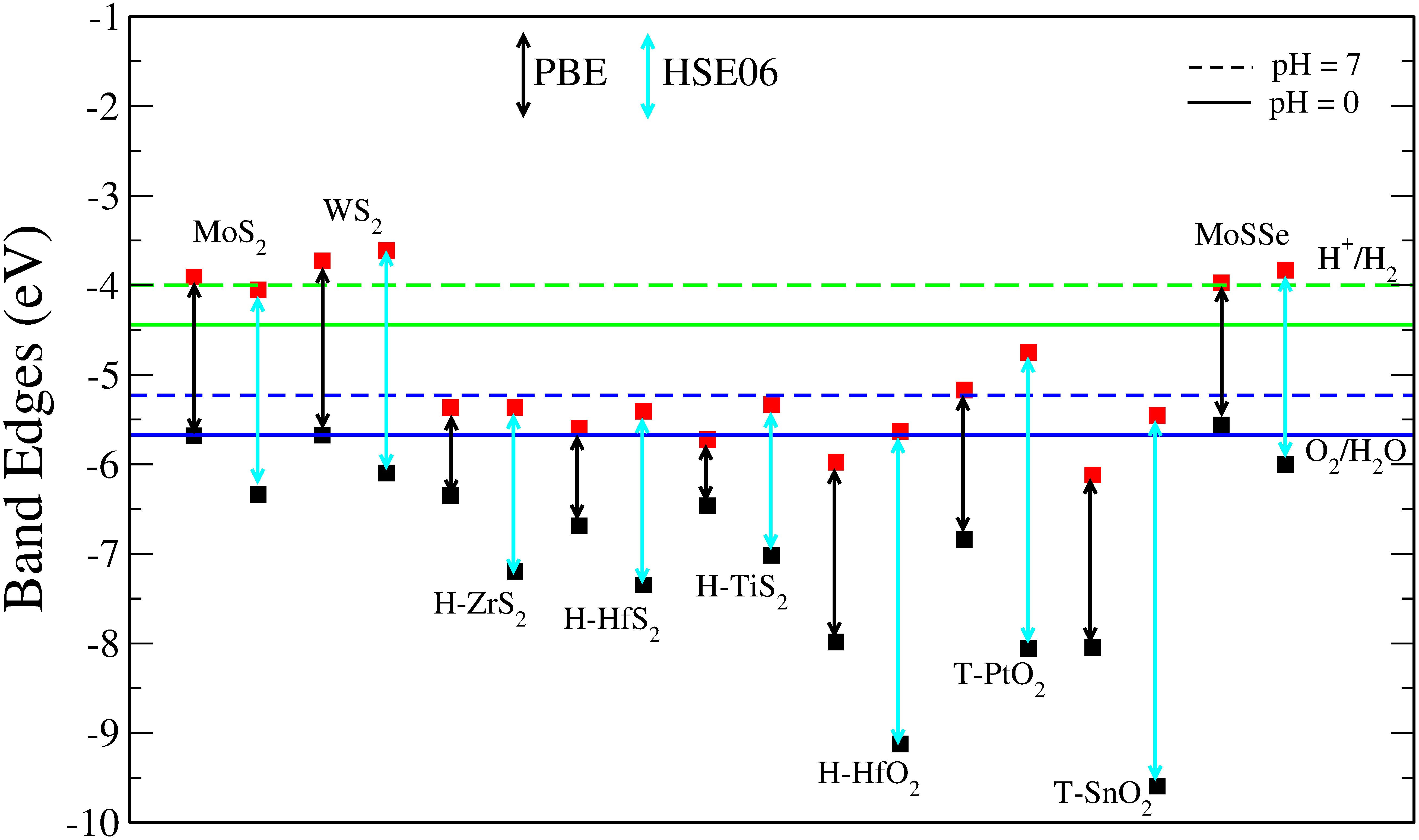 (b)
(b) (c)
(c)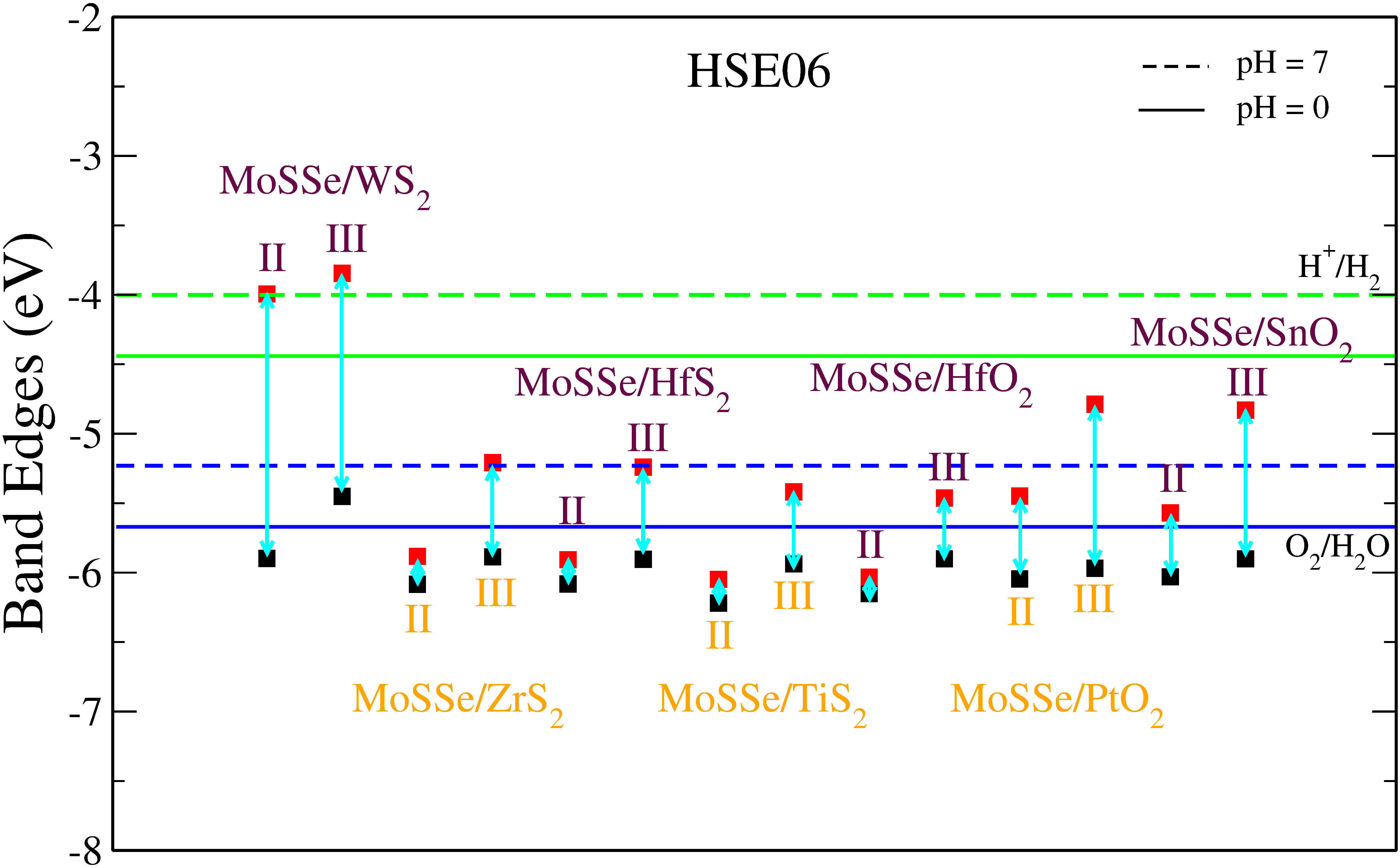
Fig. 3(b) and Fig. 3(c) depict the absolute band edge positions of the MoS2 and MoSSe based vdW HTSs, respectively. Fig. 3(b) indicates that individual band alignment approximately predicts the combined alignment of the vdW HTSs. The weak vdW interaction between 2D monolayers is attributed to the aforementioned indication. Here, the type II alignment can be seen with VBM of MoS2 (or MoSSe ) monolayer and CBm of HfS2, ZrS2, TiS2, HfO2, T-PtO2 and T-SnO2 monolayers. The band gaps of the monolayers and vdW HTSs are listed in SI (Table I). Now, the CBm and VBM should lie a few eVs above and below the redox potentials for the material to be good for photocatalysis. However, in our case the vdW HTS band gap does not straddle the photocatalytic water splitting potentials. Hence, we analyze these bilayer vdW HTSs for their applicability as Z-scheme photocatalyst. The vdW HTSs deduced for further analysis from Fig. 3 are the configurations consisting HfS2, ZrS2, TiS2, HfO2, T-PtO2 and T-SnO2. Note that MoS2 (or MoSSe) monolayer (CBm) does form type II alignment with WS2 (VBM) as well and the HTS is observed to be capable for photocatalysis (but not via Z-scheme). However, we have included this in our manuscript as a reference, with an intention to showcase clear distinction w.r.t Z-scheme photocatalysts. Moreover, on observing Fig. 3(c) a unanimously similar trend infers that the band gap of vdW HTSs of configuration II is significantly different than that of configuration III.
It should be noted that the absolute band edge alignment is obtained with respect to the zero vacuum level. The associated E (vacuum level) of each calculation is obtained from the electrostatic potential of the system. As is evident from the term, the plot explains the electrostatic potential corresponding to each atomic layer (see Fig. 4). It is pertinent to understand the plot as it informs about the work function and potential difference between the monolayers. Thus, we are able to analyze the interlayer charge transfer that indicates the photocatalytic strength. Fig. 4 corresponds to the electrostatic potential plot of MoS2/WS2. Considering left to right chronology in Fig. 4(a), we observe the potential of S, Mo, S atomic layers of MoS2 monolayer and S, W, S atomic layers of WS2 monolayer. We see a clear difference in the potentials of cationic layers viz. Mo and W atomic layers. The gradient between the monolayers facilitate the charge separation between them. Fig. 4(b) shows the corresponding MoS2/WS2 vdW HTS describing the respective atomic layers.
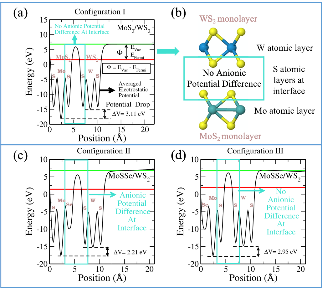
Fig. 4(c) and (d), show the plots for MoSSe/WS2 configuration II and III, respectively. We observe, that in configuration II (Fig. 4(c)) there is an additional potential gradient between Se atomic layer of MoSSe and S atomic layer of the WS2 at the interface, along with the cationic potential difference. In case of configuration III, the interface has no anionic gradient (due to presence of S in both the layers facing each other) and hence, charge separation is mainly the result of cationic gradient. Therefore, we see different band gaps in configuration III and configuration II. Further, one should always remember, that these configurations are type II and the band edge levels are on two different layers. Therefore, any potential gradient at interface will definitely effect the corresponding band edge levels. Fig. S1-S6 in SI discuss the electrostatic potential for other vdW HTSs. Fig. S4 explains the change in band gap on the basis of dipole direction. Dipole direction is seen from S to Se i.e. from lower to higher potential. So, we observe opposite dipole directions in configurations II and III, thereby affecting the interfacial interactions. Thus, the vdW HTSs with TMOs are also inline with the above discussion and inference.
| BX2 | Hirshfeld charge (e) | Work function () (eV) | ||||
|---|---|---|---|---|---|---|
| I | II | III | I | II | III | |
| WS2 | 0.64 | 0.19 | 3.00 | 5.19 | 5.34 | 4.76 |
| ZrS2 | -0.26 | -0.25 | -0.16 | 5.98 | 6.02 | 5.56 |
| HfS2 | -0.08 | -0.14 | -0.07 | 5.98 | 6.01 | 5.58 |
| TiS2 | -0.09 | -0.25 | -0.12 | 6.02 | 6.15 | 5.69 |
| HfO2 | -0.04 | -0.12 | -0.09 | 6.12 | 6.13 | 5.70 |
| T-PtO2 | 0.03 | -0.08 | -0.04 | 5.78 | 5.75 | 5.53 |
| T-SnO2 | -0.10 | -0.16 | -0.06 | 5.91 | 5.79 | 5.46 |
We have also calculated the associated charge density on the layers and the work function of the vdW HTSs. The work function () is significant parameter to understand the charge separation or transfer at the interface. It is defined as follows:
| (2) |
where E and E are the electrostatic potential corresponding to the vacuum level and Fermi level, respectively (see Fig. 4). Table 2 gives the total Hirshfeld charge (of all the atoms in the monolayer of the HTS) and the work function of vdW HTSs. The estimated values of the work function of free standing monolayer ( as in Table 5), have been corroborated with the existing literature 73***Note that the mentioned reference has considered 15 Å vacuum, which we have found to be converged at 20 Å vacuum. The slight difference (i.e. not exact match) may be due to this change.. The Hirshfeld charge in case of configuration II show greater charge transfer than that of as in the case of configuration I and III. This is attributed to the anionic and cationic potential difference at the interface. The lesser charge transfer corresponds to the lower work function in configurations I and III. The plane averaged charge density difference has been calculated (see section V in SI) by:
| (3) |
where , , and are the charge density of the vdW HTS, monolayer MoS2, monolayer MoSSe and monolayer BX2, respectively.
| BX2 | (eV) | (eV) | ||
|---|---|---|---|---|
| I | II | III | ||
| WS2 | 5.53 | -0.34 | -0.19 | -0.77 |
| ZrS2 | 6.95 | -0.97 | -0.93 | -1.39 |
| HfS2 | 7.13 | -1.15 | -1.12 | -1.55 |
| TiS2 | 7.01 | -0.99 | -0.86 | -1.32 |
| HfO2 | 8.86 | -2.74 | -2.73 | -3.16 |
| T-PtO2 | 7.86 | -2.08 | -2.11 | -2.33 |
| T-SnO2 | 9.06 | -3.15 | -3.27 | -3.60 |
We can understand the charge transfer by calculating the band bending () as well. This parameter is estimated by the Fermi-level difference between the vdW HTSs and the corresponding free-standing monolayer, with the expression as follows 76:
| (4) |
where is the work function of vdW HTSs and is the work function of free standing monolayer. The indicates charge transfer from the vdW HTSs to the monolayer. All the vdW HTSs, display i.e. charge gained by the monolayer (Table 3). The observation is in sync with the calculated Hirshfeld charges as noted in Table 2. It is to be noted that in case of WS2, is more negative with (MoS2) = 5.82 eV than that with (WS2). Hence, the associated Hirshfeld charge on the WS2 monolayer is positive. The above observations indicate MoSSe based configurations (II and III) to play a crucial role in photocatalytic applications.
The aforementioned discussions along with Fig. 3(a) have showcased the spatial charge separation due to the work function difference. Therefore, with the e- - h+ pair generation in the individual monolayers of vdW HTSs, the MoS2 (or MoSSe) monolayer will be positively charged as it contributes to the VBM of vdW HTS, which will restrict the flow of e- to other layer (BX2). Moreover, BX2 monolayer that contributes to the CBm of vdW HTS, does not straddle the reduction potential. Hence, MoS2 (or MoSSe) monolayer will observe restricted e- motion from its CBm to BX2 CBm, thereby facilitating the e- - h+ recombination path of BX2 CBm to MoS2 VBM and promoting the standard Z-scheme mechanism.
3.3 Recombination in vdW HTSs
Considering the case of photocatalysts that straddle the potentials, lesser recombination is synchronous with the effective photocatalytic capability. However, vdW HTSs for applicability as Z-scheme potocatalysts, require higher recombination in them as compared to their constituent monolayers. Hence, the layer with CBm above the reduction potential can facilitate HER, while, the layer with VBM below the oxidation potential can facilitate OER. In view of this, we have analyzed the recombination rate, which is indicated by the effective mass of electrons and holes. The effective mass has been calculated by the parabolic fitting at CBm and VBM in the bandstructure obtained by the hybrid calculations 77. The bandstructure of MoS2/ZrS2 has been found to be previously reported 78 and is in sync with that reported in the present work. The similar database of other vdW HTSs discussed here are previously unreported.
| BX2 | WS2 | ZrS2 | HfS2 | TiS2 | HfO2 | T-PtO2 | T-SnO2 |
| D | 1.29 | 1.58 | 1.17 | 0.03 | 5.88 | 4.66 | 9.00 |
| BX2 | Effective Mass Ratio (D) | ||
|---|---|---|---|
| I | II | III | |
| WS2 | 2.50 | 0.85 | 10.19 |
| ZrS2 | 0.13 | 0.64 | 0.62 |
| HfS2 | 0.65 | 0.87 | 0.71 |
| TiS2 | 0.50 | 0.20 | 0.80 |
| HfO2 | 0.32 | 0.34 | 0.34 |
| T-PtO2 | 0.49 | 0.50 | 0.49 |
| T-SnO2 | 0.91 | 1.15 | 1.14 |
The recombination in the system can be estimated by relative ratio (D) that is defined as follows 79:
| (5) |
The higher the variance of D from 1, the lesser is the recombination. Since, D refers to the relative ratio of the effective masses of hole () and electron (), its value closer to 1 (i.e low variance) is ideal for high recombination in the system. This is obvious as value closer to 1 indicates similar electron and hole effective masses, resulting in easier recombination.
On the contrary, large difference in the effective masses pose significant difference in carrier mobilities leading to the separation of carriers and hindrance in their recombination. Consider, Table 5 that enlists the value of D for monolayers and their corresponding vdW HTSs. The effective mass of carriers at CBm (i.e. ) and VBM (i.e. ) have been obtained along the designated direction in the high symmetry path - M - K - (see bandstructures i.e. Fig. S7 in SI).
Also, it should be noted that the parameter is calculated from the bandstructures of the supercell than the primitive cells. Since, the supercell is small, the density of the bands near the VBM and CBm is not very high and hence, the band folding is not an issue here.
Further, since we are considering Z-scheme photocatalysis, we require monolayer with lesser recombination as compared to that of their corresponding vdW HTSs. In order to review this we have checked the variance of D values from 1 for monolayers and vdW HTSs. Therefore, the vdW HTSs with lesser variance as compared to that of their respective monolayer can be considered probable for Z-scheme photocatalysis. As per the discussed approach, we have deduced MoSSe/ZrS2 (configuration II and III), MoSSe/HfS2 (configuration II), MoSSe/TiS2 (configuration III), MoS2/SnO2 and MoSSe/SnO2 (configuration II and III) as the probable Z-scheme vdW HTSs. Amongst these, the MoS2/SnO2, MoSSe/HfS2 (configuration II) and MoSSe/TiS2 (configuration III) have shown least variance from 1. Their respective carrier mobilities 80 are computed as 46102 cm2V-1s-1, 21102 cm2V-1s-1 and 2102 cm2V-1s-1. Additional details are provided in the supplementary material. Note that, we have also estimated their exciton binding energy (E), which showed comparatively smaller E of vdW HTSs as compared to that of MoS2 and MoSSe monolayers (see section VII in SI). It should be mentioned here that the value D is an indicative approach and should not be considered as the sole criteria for e- - h+ recombination. This yields future scope to explore more on carrier dynamics to understand the excitonic physics in these materials. We have, in addition, nevertheless, complied to the inferences with the study of optical response, carrier mobility, H2O adsorption and HER.
3.4 Absorption spectra
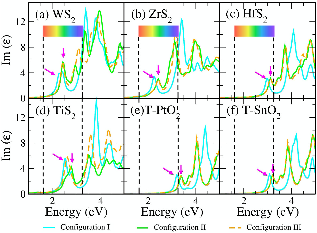
Optical response is amongst the important parameters involved in constructing the photocatalytic devices. Therefore, we have obtained the same for previously discussed vdW HTSs, that can be considered for the photocatalytic applications. Fig. 5 gives the absorption spectra obtained from imaginary part of the dielectric function as computed by GW method (G0W0@HSE06). The dielectric function is a frequency dependent complex function ( = Re() + Im()) where the real part (Re()) is computed from the Kramers-Kronig relation and the imaginary part (Im()) is obtained from the interband matrix elements in the momentum space 81. Since, the interband process consists of transitions to the unoccupied orbitals, the Im() gives the absorption spectra. The first peak will, therefore, indicate the onset of absorption process. We observe that the vdW HTSs of MoS2/TMD and MoS2/TMO have response in the visible region. The spectra corresponding to MoSSe vdW HTSs (configuration II and III) have shown minute blue shift as compared to that of MoS2 vdW HTSs. Further, we observe from Fig. 5(b) that the vdW HTSs with ZrS2 and TiS2 monolayer show red shift as compared to other vdW HTSs (i.e., Fig. 5(a), (c), (d)-(f)). The spectra, thus, indicate the use of MoS2/ZrS2, MoSSe/ZrS2, MoS2/TiS2 and MoSSe/TiS2 for harnessing the overlap region of Im() with the solar spectrum in order to construct the photocatalytic devices.
3.5 H2O Adsorption
| BX2 | E (eV) | Distance (Å) |
|---|---|---|
| WS2 | -0.09 | 2.88 |
| ZrS2 | -0.24 | 2.59 |
| HfS2 | -0.23 | 2.75 |
| TiS2 | -0.25 | 2.74 |
| T-PtO2 | -0.28 | 2.08 |
| T-SnO2 | -0.29 | 2.31 |
We have further calculated the H2O adsorption in these vdW HTSs to confirm that the adsorption is supported for further redox reactions. The associated expression is as given:
| (6) |
where, E is the adsorption energy (see Table 6) of the H2O on the vdW HTSs; E(adsorbed HO) is the energy of the vdW HTSs with adsorbed H2O, E(vdW HTSs) is the energy of the vdW HTSs and E(H2O) is the energy of the water molecule. From the Table 6 we observe, H2O is physisorbed in the system and its binding strength in all the monolayers is higher than that in case of WS2. Also, the transition metal oxides show higher binding strength than the transition metal dichalcogenides. The data supplement the analysis for considering the monolayers for Z-scheme photocatalysis.
In addition, we have calculated the Gibb’s free energy change (G) of the intermediate in the HER as per the expression:
| (7) |
where E is the intermediate adsorption energy on the vdW HTSs, E is the change in zero-point energy and S is the difference of entropy. The temperature, T, is taken as 300K. We have calculated the E and TS by the following expression using Density Functional Perturbation Theory (DFPT):
| (8) |
| (9) |
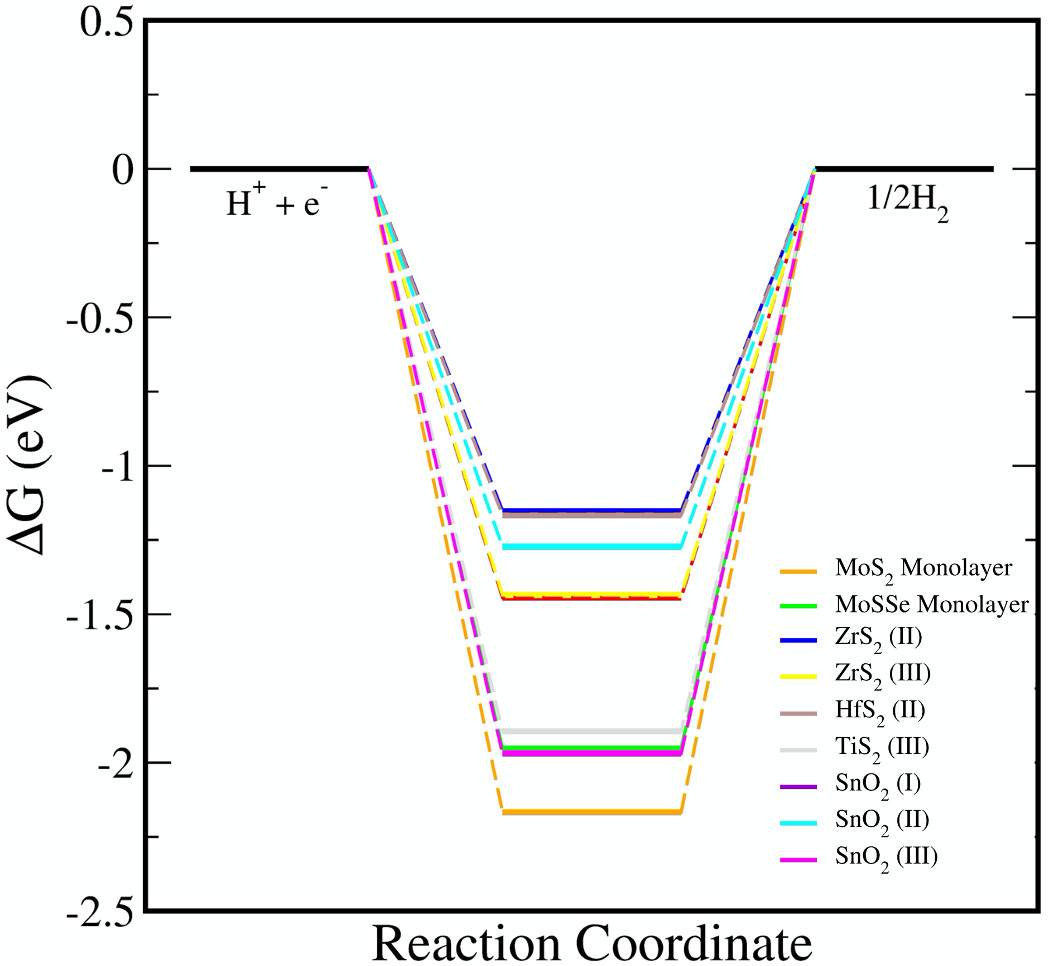
where h is Planck’s constant, is vibrational frequencies and is Boltzmann constant. The HER diagram along the reaction pathway H+ + e- H* 1/2 H2 is illustrated in the Fig. 6. Here, H* represents the adsorbed intermediate. Under the consideration of pH = 0 and Standard Hydrogen Electrode (SHE) potential of 0 V the H+ + e- is equivalent to the 1/2 H2.
Now, upon systematically revisiting all the aforementioned factors, we have observed vdW HTSs to be type II with their work function being affected by the interfacial potential difference. This further influences the charge separation. Another point is that the smaller conduction band offset between the two monolayer systems would promote efficient charge separation at the interface 82. Therefore, in reference to Fig. 3, with comparatively large difference in two conduction band levels along with type II alignment, the consideration for interlayer recombination in vdW HTSs for Z-scheme process seems very much plausible. Effective mass being the important factor for the same, we have indicated the recombination probability by the effective mass ratio (D). However, since this approach is qualitative we have explicitly included the results of optical response, H2O adsorption and HER as direct evidences to validate MoSSe/HfS2, MoSSe/TiS2, MoS2/T-SnO2, MoSSe/T-SnO2, MoS2/ZrS2 and MoSSe/ZrS2 are probable Z-scheme photocatalysts.
4 Conclusion
An exhaustive study has been undertaken for understanding different MoS2 and MoSSe based vdW HTSs. As per the band edge alignment, it is observed that these vdW HTSs do not facilitate the normal photocatalytic process as they do not straddle the redox potential. However, these are predicted to be implementing the natural photocatalysis by Z-scheme. The band edge alignment of the MoSSe vdW HTSs has inferred large band gap in configuration III than in case of configuration II. This has been attributed to the additional anionic potential gradient due to Se atomic layer at the interface in configuration II. The probability of recombination as implicated by the effective mass ratio (D) has corroborated the MoSSe/HfS2, MoSSe/TiS2, MoS2/T-SnO2, MoSSe/T-SnO2, MoS2/ZrS2 and MoSSe/ZrS2 as favourable Z-scheme photocatalyst. The absorption spectra further confirm the visible light response of these vdW HTSs and hence, their applicability in the photocatalytic devices. Finally, the H2O adsorption and HER indicate their interaction with water to help in the photocatalytic process.
5 Supporting Information
(I) Electrostatic Potential. (II) Lattice Parameters. (III) Band Gaps of Configurations. (IV) Bandstructures of Z-scheme vdW HTSs. (V) Planar Averaged Charged Density. (VI) Absorption Spectra of Monolayers. (VII) Exciton Binding Energy (VIII) Carrier Mobility.
6 Acknowledgement
AS acknowledges IIT Delhi for the financial support. AS and MJ thank Pooja Basera for helpful discussions. MJ acknowledges CSIR, India, for the senior research fellowship [grant no. 09/086(1344)/2018-EMR-I]. SB acknowledges the financial support SERB under his Core Research Grant [CRG/2019/000647]. We acknowledge the High Performance Computing (HPC) facility at IIT Delhi for computational resources.
References
- Ni et al. 2007 Ni, M.; Leung, M. K.; Leung, D. Y.; Sumathy, K. A review and recent developments in photocatalytic water-splitting using TiO2 for hydrogen production. Renewable and Sustainable Energy Reviews 2007, 11, 401–425
- Yao et al. 2015 Yao, H.; Fan, M.; Wang, Y.; Luo, G.; Fei, W. Magnetic titanium dioxide based nanomaterials: synthesis, characteristics, and photocatalytic application in pollutant degradation. Journal of Materials Chemistry A 2015, 3, 17511–17524
- Opoku et al. 2017 Opoku, F.; Govender, K. K.; van Sittert, C. G. C. E.; Govender, P. P. Role of MoS 2 and WS 2 monolayers on photocatalytic hydrogen production and the pollutant degradation of monoclinic BiVO 4: A first-principles study. New Journal of Chemistry 2017, 41, 11701–11713
- Yu et al. 2019 Yu, C.; Chen, F.; Zeng, D.; Xie, Y.; Zhou, W.; Liu, Z.; Wei, L.; Yang, K.; Li, D. A facile phase transformation strategy for fabrication of novel Z-scheme ternary heterojunctions with efficient photocatalytic properties. Nanoscale 2019, 11, 7720–7733
- Gupta et al. 2015 Gupta, A.; Sakthivel, T.; Seal, S. Recent development in 2D materials beyond graphene. Progress in Materials Science 2015, 73, 44–126
- Singh et al. 2020 Singh, A.; Basera, P.; Saini, S.; Kumar, M.; Bhattacharya, S. Importance of Many-Body Dispersion in the Stability of Vacancies and Antisites in Free-Standing Monolayer of MoS2 from First-Principles Approaches. The Journal of Physical Chemistry C 2020, 124, 1390–1397
- Chen et al. 2018 Chen, Y.; Huang, S.; Ji, X.; Adepalli, K.; Yin, K.; Ling, X.; Wang, X.; Xue, J.; Dresselhaus, M.; Kong, J., et al. Tuning electronic structure of single layer MoS2 through defect and interface engineering. ACS nano 2018, 12, 2569–2579
- Rao et al. 2015 Rao, C.; Gopalakrishnan, K.; Maitra, U. Comparative study of potential applications of graphene, MoS2, and other two-dimensional materials in energy devices, sensors, and related areas. ACS applied materials & interfaces 2015, 7, 7809–7832
- Singh et al. 2019 Singh, E.; Singh, P.; Kim, K. S.; Yeom, G. Y.; Nalwa, H. S. Flexible molybdenum disulfide (MoS2) atomic layers for wearable electronics and optoelectronics. ACS applied materials & interfaces 2019, 11, 11061–11105
- Zeng et al. 2013 Zeng, H.; Liu, G.-B.; Dai, J.; Yan, Y.; Zhu, B.; He, R.; Xie, L.; Xu, S.; Chen, X.; Yao, W., et al. Optical signature of symmetry variations and spin-valley coupling in atomically thin tungsten dichalcogenides. Scientific reports 2013, 3, 1608
- Wang and Guo 2015 Wang, C.-Y.; Guo, G.-Y. Nonlinear optical properties of transition-metal dichalcogenide MX2 (M= Mo, W; X= S, Se) monolayers and trilayers from first-principles calculations. The Journal of Physical Chemistry C 2015, 119, 13268–13276
- Glebko et al. 2018 Glebko, N.; Aleksandrova, I.; Tewari, G. C.; Tripathi, T. S.; Karppinen, M.; Karttunen, A. J. Electronic and vibrational properties of TiS2, ZrS2, and HfS2: Periodic trends studied by dispersion-corrected hybrid density functional methods. The Journal of Physical Chemistry C 2018, 122, 26835–26844
- Lau et al. 2019 Lau, K. W.; Cocchi, C.; Draxl, C. Electronic and optical excitations of two-dimensional ZrS 2 and HfS 2 and their heterostructure. Physical Review Materials 2019, 3, 074001
- Mattinen et al. 2019 Mattinen, M.; Popov, G.; Vehkamäki, M.; King, P. J.; Mizohata, K.; Jalkanen, P.; Räisänen, J.; Leskelä, M.; Ritala, M. Atomic layer deposition of emerging 2D semiconductors, HfS2 and ZrS2, for optoelectronics. Chemistry of Materials 2019, 31, 5713–5724
- Lebègue et al. 2013 Lebègue, S.; Björkman, T.; Klintenberg, M.; Nieminen, R. M.; Eriksson, O. Two-dimensional materials from data filtering and ab initio calculations. Physical Review X 2013, 3, 031002
- Yang et al. 2019 Yang, J.; Zeng, Z.; Kang, J.; Betzler, S.; Czarnik, C.; Zhang, X.; Ophus, C.; Yu, C.; Bustillo, K.; Pan, M., et al. Formation of two-dimensional transition metal oxide nanosheets with nanoparticles as intermediates. Nature materials 2019, 18, 970–976
- Leong et al. 2016 Leong, C. C.; Pan, H.; Ho, S. K. Two-dimensional transition-metal oxide monolayers as cathode materials for Li and Na ion batteries. Physical Chemistry Chemical Physics 2016, 18, 7527–7534
- Liao and Carter 2013 Liao, P.; Carter, E. A. New concepts and modeling strategies to design and evaluate photo-electro-catalysts based on transition metal oxides. Chemical Society Reviews 2013, 42, 2401–2422
- Ju et al. 2020 Ju, L.; Bie, M.; Shang, J.; Tang, X.; Kou, L. Janus transition metal dichalcogenides: A superior platform for photocatalytic water splitting. Journal of Physics: Materials 2020, 3, 022004
- Sun et al. 2018 Sun, Y.; Shuai, Z.; Wang, D. Janus monolayer of WSeTe, a new structural phase transition material driven by electrostatic gating. Nanoscale 2018, 10, 21629–21633
- Song et al. 2019 Song, B.; Liu, L.; Yam, C. Suppressed Carrier Recombination in Janus MoSSe Bilayer Stacks: A Time-Domain Ab Initio Study. The journal of physical chemistry letters 2019, 10, 5564–5570
- Sun and Schwingenschlogl 2020 Sun, M.; Schwingenschlogl, U. B2P6: A Two-dimensional anisotropic Janus material with potential in photocatalytic water splitting and metal-ion batteries. Chemistry of Materials 2020, 32, 4795–4800
- Ma et al. 2018 Ma, X.; Wu, X.; Wang, H.; Wang, Y. A Janus MoSSe monolayer: a potential wide solar-spectrum water-splitting photocatalyst with a low carrier recombination rate. Journal of Materials Chemistry A 2018, 6, 2295–2301
- Luo et al. 2020 Luo, Y.; Wang, S.; Shu, H.; Chou, J.-P.; Ren, K.; Yu, J.; Sun, M. A MoSSe/blue phosphorene vdw heterostructure with energy conversion efficiency of 19.9% for photocatalytic water splitting. Semiconductor Science and Technology 2020, 35, 125008
- Kuc and Heine 2015 Kuc, A.; Heine, T. The electronic structure calculations of two-dimensional transition-metal dichalcogenides in the presence of external electric and magnetic fields. Chemical Society Reviews 2015, 44, 2603–2614
- Kumar et al. 2018 Kumar, R.; Verzhbitskiy, I.; Giustiniano, F.; Sidiropoulos, T. P.; Oulton, R. F.; Eda, G. Interlayer screening effects in WS2/WSe2 van der Waals hetero-bilayer. 2D Materials 2018, 5, 041003
- Huang et al. 2017 Huang, Y.; Chen, X.; Wang, C.; Peng, L.; Qian, Q.; Wang, S. Layer-dependent electronic properties of phosphorene-like materials and phosphorene-based van der Waals heterostructures. Nanoscale 2017, 9, 8616–8622
- Terrones et al. 2013 Terrones, H.; López-Urías, F.; Terrones, M. Novel hetero-layered materials with tunable direct band gaps by sandwiching different metal disulfides and diselenides. Scientific reports 2013, 3, 1–7
- Zhang and Schwingenschlögl 2018 Zhang, Q.; Schwingenschlögl, U. Rashba effect and enriched spin-valley coupling in Ga X/M X 2 (M= Mo, W; X= S, Se, Te) heterostructures. Physical Review B 2018, 97, 155415
- Rivera et al. 2016 Rivera, P.; Seyler, K. L.; Yu, H.; Schaibley, J. R.; Yan, J.; Mandrus, D. G.; Yao, W.; Xu, X. Valley-polarized exciton dynamics in a 2D semiconductor heterostructure. Science 2016, 351, 688–691
- Li et al. 2018 Li, P.; Zhang, W.; Li, D.; Liang, C.; Zeng, X. C. Multifunctional Binary Monolayers Ge x P y: Tunable Band Gap, Ferromagnetism, and Photocatalyst for Water Splitting. ACS applied materials & interfaces 2018, 10, 19897–19905
- Li et al. 2019 Li, P.; Zhang, W.; Liang, C.; Zeng, X. C. Two-dimensional MgX 2 Se 4 (X= Al, Ga) monolayers with tunable electronic properties for optoelectronic and photocatalytic applications. Nanoscale 2019, 11, 19806–19813
- Luo et al. 2019 Luo, Y.; Ren, K.; Wang, S.; Chou, J.-P.; Yu, J.; Sun, Z.; Sun, M. First-principles study on transition-metal dichalcogenide/BSe van der Waals heterostructures: A promising water-splitting photocatalyst. The Journal of Physical Chemistry C 2019, 123, 22742–22751
- Luo et al. 2019 Luo, Y.; Wang, S.; Ren, K.; Chou, J.-P.; Yu, J.; Sun, Z.; Sun, M. Transition-metal dichalcogenides/Mg (OH) 2 van der Waals heterostructures as promising water-splitting photocatalysts: a first-principles study. Physical Chemistry Chemical Physics 2019, 21, 1791–1796
- Ren et al. 2020 Ren, K.; Wang, S.; Luo, Y.; Chou, J.-P.; Yu, J.; Tang, W.; Sun, M. High-efficiency photocatalyst for water splitting: a Janus MoSSe/XN (X= Ga, Al) van der Waals heterostructure. Journal of Physics D: Applied Physics 2020, 53, 185504
- Wang et al. 2018 Wang, S.; Ren, C.; Tian, H.; Yu, J.; Sun, M. MoS 2/ZnO van der Waals heterostructure as a high-efficiency water splitting photocatalyst: a first-principles study. Physical Chemistry Chemical Physics 2018, 20, 13394–13399
- Li et al. 2013 Li, Y.; Li, Y.-L.; Araujo, C. M.; Luo, W.; Ahuja, R. Single-layer MoS 2 as an efficient photocatalyst. Catalysis Science & Technology 2013, 3, 2214–2220
- Parzinger et al. 2015 Parzinger, E.; Miller, B.; Blaschke, B.; Garrido, J. A.; Ager, J. W.; Holleitner, A.; Wurstbauer, U. Photocatalytic stability of single-and few-layer MoS2. ACS nano 2015, 9, 11302–11309
- Tang et al. 2016 Tang, Z.-K.; Yin, W.-J.; Zhang, L.; Wen, B.; Zhang, D.-Y.; Liu, L.-M.; Lau, W.-M. Spatial separation of photo-generated electron-hole pairs in BiOBr/BiOI bilayer to facilitate water splitting. Scientific reports 2016, 6, 32764
- Gao et al. 2019 Gao, X.; Shen, Y.; Ma, Y.; Wu, S.; Zhou, Z. A water splitting photocatalysis: blue phosphorus/g-GeC van der Waals heterostructure. Applied Physics Letters 2019, 114, 093902
- Zhang et al. 2018 Zhang, R.; Zhang, L.; Zheng, Q.; Gao, P.; Zhao, J.; Yang, J. Direct Z-scheme water splitting photocatalyst based on two-dimensional Van Der Waals heterostructures. The journal of physical chemistry letters 2018, 9, 5419–5424
- Ren et al. 2019 Ren, K.; Ren, C.; Luo, Y.; Xu, Y.; Yu, J.; Tang, W.; Sun, M. Using van der Waals heterostructures based on two-dimensional blue phosphorus and XC (X= Ge, Si) for water-splitting photocatalysis: a first-principles study. Physical Chemistry Chemical Physics 2019, 21, 9949–9956
- Wang et al. 2018 Wang, B.-J.; Li, X.-H.; Zhao, R.; Cai, X.-L.; Yu, W.-Y.; Li, W.-B.; Liu, Z.-S.; Zhang, L.-W.; Ke, S.-H. Electronic structures and enhanced photocatalytic properties of blue phosphorene/BSe van der Waals heterostructures. Journal of Materials Chemistry A 2018, 6, 8923–8929
- Fu et al. 2016 Fu, C.-F.; Luo, Q.; Li, X.; Yang, J. Two-dimensional van der Waals nanocomposites as Z-scheme type photocatalysts for hydrogen production from overall water splitting. Journal of Materials Chemistry A 2016, 4, 18892–18898
- Liu et al. 2020 Liu, Y.; Zeng, X.; Easton, C. D.; Li, Q.; Xia, Y.; Yin, Y.; Hu, X.; Hu, J.; Xia, D.; McCarthy, D. T., et al. An in situ assembled WO 3–TiO 2 vertical heterojunction for enhanced Z-scheme photocatalytic activity. Nanoscale 2020, 12, 8775–8784
- Xia et al. 2019 Xia, X.; Song, M.; Wang, H.; Zhang, X.; Sui, N.; Zhang, Q.; Colvin, V. L.; William, W. Y. Latest progress in constructing solid-state Z scheme photocatalysts for water splitting. Nanoscale 2019, 11, 11071–11082
- Maeda 2013 Maeda, K. Z-scheme water splitting using two different semiconductor photocatalysts. ACS Catalysis 2013, 3, 1486–1503
- Li et al. 2016 Li, H.; Tu, W.; Zhou, Y.; Zou, Z. Z-Scheme photocatalytic systems for promoting photocatalytic performance: recent progress and future challenges. Advanced Science 2016, 3, 1500389
- Bard 1979 Bard, A. J. Photoelectrochemistry and heterogeneous photocatalysis at semiconductors. Journal of Photochemistry 1979, 10, 59–75
- Lang and Hu 2020 Lang, J.; Hu, Y. H. Phosphorus-based metal-free Z-scheme 2D van der Waals heterostructures for visible-light photocatalytic water splitting: a first-principles study. Physical Chemistry Chemical Physics 2020, 22, 9250–9256
- Ju et al. 2018 Ju, L.; Dai, Y.; Wei, W.; Li, M.; Huang, B. DFT investigation on two-dimensional GeS/WS2 van der Waals heterostructure for direct Z-scheme photocatalytic overall water splitting. Applied Surface Science 2018, 434, 365–374
- Rasmussen and Thygesen 2015 Rasmussen, F. A.; Thygesen, K. S. Computational 2D materials database: electronic structure of transition-metal dichalcogenides and oxides. The Journal of Physical Chemistry C 2015, 119, 13169–13183
- Martin 2004 Martin, R. M. Electronic structure: basic theory and practical methods; Cambridge university press, 2004
- Martin et al. 2016 Martin, R. M.; Reining, L.; Ceperley, D. M. Interacting Electrons; Cambridge University Press, 2016
- Freysoldt et al. 2014 Freysoldt, C.; Grabowski, B.; Hickel, T.; Neugebauer, J.; Kresse, G.; Janotti, A.; Van de Walle, C. G. First-principles calculations for point defects in solids. Reviews of modern physics 2014, 86, 253
- Feng et al. 2014 Feng, L.-p.; Su, J.; Chen, S.; Liu, Z.-t. First-principles investigations on vacancy formation and electronic structures of monolayer MoS2. Materials Chemistry and Physics 2014, 148, 5–9
- Hohenberg and Kohn 1964 Hohenberg, P.; Kohn, W. Inhomogeneous electron gas. Physical review 1964, 136, B864
- Kohn and Sham 1965 Kohn, W.; Sham, L. J. Self-consistent equations including exchange and correlation effects. Physical review 1965, 140, A1133
- Kresse and Furthmüller 1996 Kresse, G.; Furthmüller, J. Efficient iterative schemes for ab initio total-energy calculations using a plane-wave basis set. Physical review B 1996, 54, 11169
- Blöchl 1994 Blöchl, P. E. Projector augmented-wave method. Physical review B 1994, 50, 17953
- Blum et al. 2009 Blum, V.; Gehrke, R.; Hanke, F.; Havu, P.; Havu, V.; Ren, X.; Reuter, K.; Scheffler, M. Ab initio molecular simulations with numeric atom-centered orbitals. Computer Physics Communications 2009, 180, 2175–2196
- Stampfl and Van de Walle 1999 Stampfl, C.; Van de Walle, C. Density-functional calculations for III-V nitrides using the local-density approximation and the generalized gradient approximation. Physical Review B 1999, 59, 5521
- Perdew et al. 1996 Perdew, J. P.; Burke, K.; Ernzerhof, M. Generalized gradient approximation made simple. Physical review letters 1996, 77, 3865
- Heyd et al. 2003 Heyd, J.; Scuseria, G. E.; Ernzerhof, M. Hybrid functionals based on a screened Coulomb potential. The Journal of chemical physics 2003, 118, 8207–8215
- Tkatchenko and Scheffler 2009 Tkatchenko, A.; Scheffler, M. Accurate molecular van der Waals interactions from ground-state electron density and free-atom reference data. Physical review letters 2009, 102, 073005
- Tkatchenko et al. 2012 Tkatchenko, A.; DiStasio Jr, R. A.; Car, R.; Scheffler, M. Accurate and efficient method for many-body van der Waals interactions. Physical review letters 2012, 108, 236402
- Weng and Gao 2018 Weng, J.; Gao, S.-P. A honeycomb-like monolayer of HfO 2 and the calculation of static dielectric constant eliminating the effect of vacuum spacing. Physical Chemistry Chemical Physics 2018, 20, 26453–26462
- Ren et al. 2020 Ren, K.; Tang, W.; Sun, M.; Cai, Y.; Cheng, Y.; Zhang, G. A direct Z-scheme PtS 2/arsenene van der Waals heterostructure with high photocatalytic water splitting efficiency. Nanoscale 2020, 12, 17281–17289
- Onida et al. 2002 Onida, G.; Reining, L.; Rubio, A. Electronic excitations: density-functional versus many-body Green’s-function approaches. Reviews of modern physics 2002, 74, 601
- Jiang et al. 2012 Jiang, H.; Rinke, P.; Scheffler, M. Electronic properties of lanthanide oxides from the G W perspective. Physical Review B 2012, 86, 125115
- Rahman et al. 2018 Rahman, A. U.; Morbec, J. M.; Rahman, G.; Kratzer, P. Commensurate versus incommensurate heterostructures of group-III monochalcogenides. Physical Review Materials 2018, 2, 094002
- Bastos et al. 2019 Bastos, C. M.; Besse, R.; Da Silva, J. L.; Sipahi, G. M. Ab initio investigation of structural stability and exfoliation energies in transition metal dichalcogenides based on Ti-, V-, and Mo-group elements. Physical Review Materials 2019, 3, 044002
- Haastrup et al. 2018 Haastrup, S.; Strange, M.; Pandey, M.; Deilmann, T.; Schmidt, P. S.; Hinsche, N. F.; Gjerding, M. N.; Torelli, D.; Larsen, P. M.; Riis-Jensen, A. C., et al. The Computational 2D Materials Database: high-throughput modeling and discovery of atomically thin crystals. 2D Materials 2018, 5, 042002
- Xia et al. 2018 Xia, C.; Xiong, W.; Xiao, W.; Du, J.; Fang, L.; Li, J.; Jia, Y. Enhanced carrier concentration and electronic transport by inserting graphene into van der Waals heterostructures of transition-metal dichalcogenides. Physical Review Applied 2018, 10, 024028
- Hu et al. 2016 Hu, X.; Kou, L.; Sun, L. Stacking orders induced direct band gap in bilayer MoSe 2-WSe 2 lateral heterostructures. Scientific reports 2016, 6, 31122
- Padilha et al. 2015 Padilha, J.; Fazzio, A.; da Silva, A. J. van der Waals heterostructure of phosphorene and graphene: tuning the Schottky barrier and doping by electrostatic gating. Physical review letters 2015, 114, 066803
- Ganose et al. 2018 Ganose, A.; Jackson, A.; Scanlon, D. sumo: Command-line tools for plotting and analysis of periodic* ab initio* calculations. Journal of Open Source Software 2018, 3, 717
- Lu et al. 2017 Lu, A. K. A.; Houssa, M.; Luisier, M.; Pourtois, G. Impact of Layer Alignment on the Behavior of MoS 2- ZrS 2 Tunnel Field-Effect Transistors: An Ab Initio Study. Physical Review Applied 2017, 8, 034017
- Zhang et al. 2012 Zhang, H.; Liu, L.; Zhou, Z. First-principles studies on facet-dependent photocatalytic properties of bismuth oxyhalides (BiOXs). RSC advances 2012, 2, 9224–9229
- Dai and Zeng 2015 Dai, J.; Zeng, X. C. Titanium trisulfide monolayer: theoretical prediction of a new direct-gap semiconductor with high and anisotropic carrier mobility. Angewandte Chemie 2015, 127, 7682–7686
- Basera et al. 2019 Basera, P.; Saini, S.; Bhattacharya, S. Self energy and excitonic effect in (un) doped TiO 2 anatase: a comparative study of hybrid DFT, GW and BSE to explore optical properties. Journal of Materials Chemistry C 2019, 7, 14284–14293
- Khanchandani et al. 2014 Khanchandani, S.; Srivastava, P. K.; Kumar, S.; Ghosh, S.; Ganguli, A. K. Band gap engineering of ZnO using core/shell morphology with environmentally benign Ag2S sensitizer for efficient light harvesting and enhanced visible-light photocatalysis. Inorganic Chemistry 2014, 53, 8902–8912