Quantum spin Hall edge states and interlayer coupling in twisted-bilayer WTe2
The quantum spin Hall (QSH) effect, characterized by topologically protected spin-polarized edge states, was recently demonstrated in monolayers of the transition metal dichalcogenide (TMD) WTe2. However, the robustness of this topological protection remains largely unexplored in van der Waals heterostructures containing one or more layers of a QSH insulator. In this work, we use scanning tunneling microscopy and spectroscopy (STM/STS) to explore the topological nature of twisted bilayer (tBL) WTe2 which is produced from folded monolayers, as well as, tear-and-stack fabrication. At the tBL bilayer edge, we observe the characteristic spectroscopic signature of the QSH edge state that is absent in topologically trivial as-grown bilayer. For small twist angles, a rectangular moiré pattern develops, which results in local modifications of the band structure. Using first principles calculations, we quantify the interactions in tBL WTe2 and its topological edge states as function of interlayer distance and conclude that it is possible to tune the topology of WTe2 bilayers via the twist angle as well as interlayer interactions.
The variety of layered two-dimensional (2D) materials available for isolation and fabrication into van der Waals heterostructures provides almost endless combinations for device engineering [1]. 1T’-TMDs have attracted recent attention among the layered materials following the prediction of the QSH edge state in the monolayer (ML) limit [2]. In particular, WTe2 has been of great interest due to its realization of multiple exotic physical phenomena depending on its thickness. Monolayer WTe2 has been reported to exhibit the predicted QSH effect, which persists up to [3, 4, 5, 6]. WTe2 monolayers further host a superconducting phase below K when electrostatically gated into the conduction band [7, 8]. Bilayer (BL) WTe2 on the other hand is predicted to be a topologically trivial semi-metal [9] which has also been shown to exhibit ferroelectric switching when a surface normal electric field is applied [10]. In the bulk limit, WTe2 was reported to be a type-II Weyl semi-metal and higher order topological insulator with 1D hinge states [11, 12]. The high degree of layer tunability in WTe2 makes it an attractive candidate for integration in van der Waals heterostructures, e.g. to realize one-dimensional topological superconductivity [13]. However, there are open questions, such as the effect of coupling to neighboring layers on the topological properties, which have to be thoroughly understood for applications of the topological edge states in electronic devices.
Recently, the interactions between rotationally misaligned layers of 2D materials have attracted attention as hosts of a variety of interesting highly-correlated phenomena such as insulating states, superconductivity, and unique topological phases [14, 15, 16, 17, 18, 19]. While most studies of twisted bilayers seek to achieve highly-correlated states through a moiré pattern in which flat bands emerge in the electronic structure [14, 15, 20, 17, 19, 21, 22], here we focus on the effects of interlayer coupling on the already present QSH edge state in ML WTe2. We find that for incommensurately stacked twisted bilayer WTe2, both layers retain their topology, which results in two sets of QSH edge states sitting on top of each other. We experimentally study the edge states and interlayer coupling for multiple twist angles and rationalize our results based on first-principles calculations, demonstrating the robust topological protection of the QSH edge state predicted in the literature [23]. In contrast to twisted bilayers, we do not observe an edge state feature at the topologically trivial as-grown bilayer WTe2 edge. The topologically trivial nature of bilayer WTe2 is supported by our observation of a QSH edge state in monolayer WTe2 at a monolayer-bilayer junction.
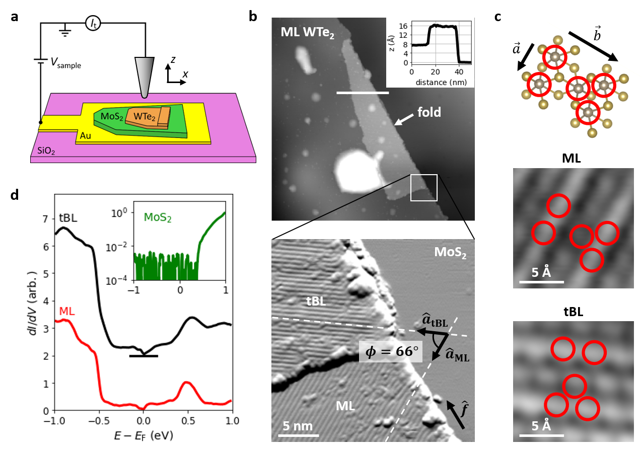
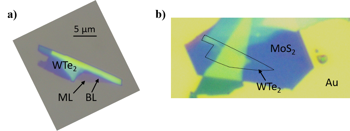
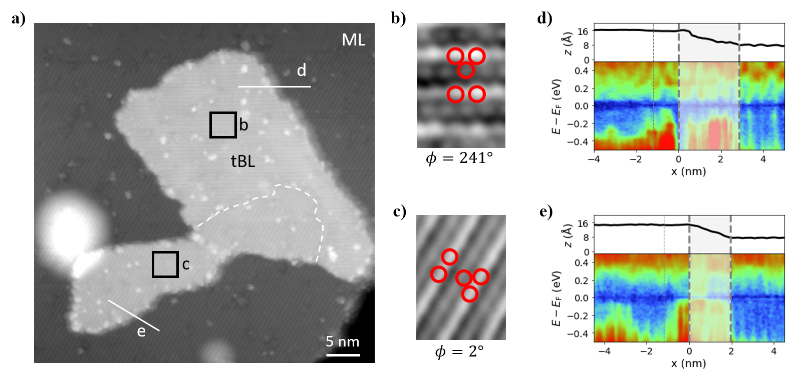
To explore the QSH edge state in exfoliated WTe2, we study WTe2/MoS2 heterostructures (Fig. 1a). Samples are fabricated using a recently developed dry-transfer flip technique that allows the stacking of van der Waals materials while maintaining atomically clean surfaces and interfaces (for details see Materials and Methods, section S1 and Ref. 13). MoS2 is used as a substrate flake to provide an atomically flat support for the WTe2. The typical signature of the WTe2 QSH edge state in the energy range () is located in the MoS2 band gap, so that substrate effects can be excluded when analyzing the edge state spectra. In addition, we can tunnel into the MoS2 conduction band at a sample bias of , allowing us to safely scan over the edge of the WTe2 flakes.
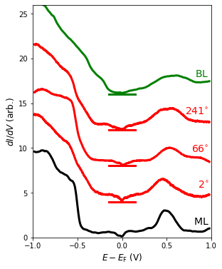
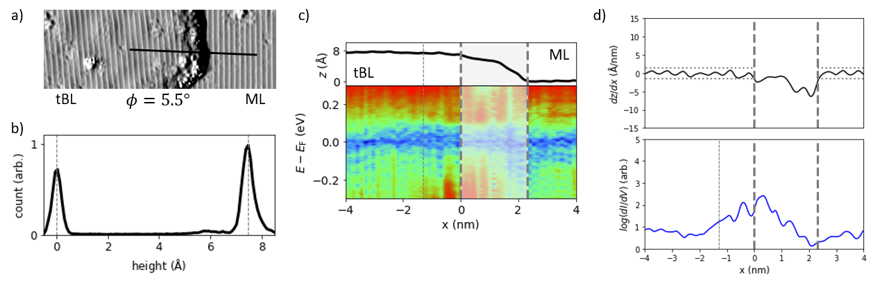
In large area scans of the heterostructures, we find random folds along the edge of the WTe2 monolayer (Fig. 1b). Such folds occur by coincidence during the exfoliation and dry-transfer and are usually undesired, e.g. for fabrication of transport devices. However, the fold offers a unique opportunity to study the interaction between the QSH edge states, which are naturally located right on top of one another along the fold. A profile across the folded region shows a ML step height of Å, i.e. slightly larger than for WTe2 monolayers on graphene or NbSe2 [4, 13] which we attribute to the electronic contrast between the respective substrate materials and the WTe2. The step height from the first to the second WTe2 layers is also Å, which slightly deviates from the as-grown bilayer step height (Å [24, 13]). This deviation can be explained by the incommensurate stacking of the rotationally misaligned layers, resulting in a larger interlayer separation. We note that the folding of the WTe2 monolayer, due to its resemblance of a screw transformation, in combination with the monolayer 1T’ crystal screw symmetry, [9], results in a bilayer that is identical to two monolayers stacked on top of each other with a twist angle , which is determined by the orientation of the fold with respect to the lattice vectors (see section S2). Using atomic resolution images of the ML and folded region (Fig. 1c), we determine the relative twist angle between the two layers to be , where is the fold axis orientation. For reference, as-grown bilayer WTe2 corresponds to by this definition. As a result of the large twist angle, we do not observe a pronounced moiré pattern and spectra taken on the folded region are almost identical to that of monolayer WTe2, indicating decoupled layers (Fig. 1d). This observation implies that there should be two independent sets of QSH edge states, one in each layer, which we explore in the following.
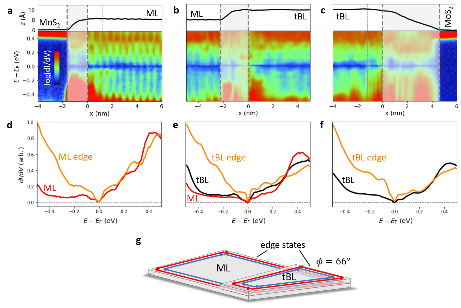
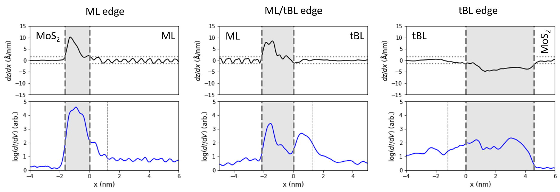
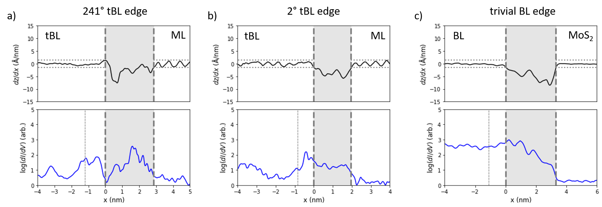
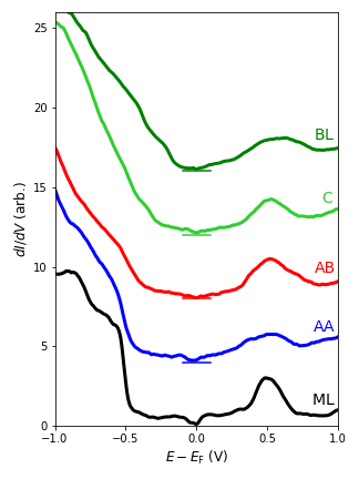
First, we examine the ML WTe2 edge (Fig. 2a), where we find the typical spectroscopic signature of the QSH edge state, in the form of an enhanced density of states below , in agreement with the literature [24, 4, 13]. The QSH edge state is observed on the flat terrace next to the onset of the topographic step edge, which distinguishes it from edge effects, such as edge reconstructions, and tip artifacts that can occur in the transition region due to the finite tip size. We systematically identify the positions of the topographic edges – namely, and the extension of the transition regions in Figs. 2a,b,c and 3c,d – as the points where the topography gradient reaches a threshold value of (see section S6 for details). Using this detection scheme, we find that the spatial extent of the QSH edge state on the ML WTe2 terrace is , in agreement with that observed in WTe2 on graphene [4] and on NbSe2 [13] and similar to what has been predicted theoretically [25].
Turning now to the ML-tBL edge, we observe a similarly enhanced density of states, which again extends from the step edge (Fig. 2b), indicating the presence of an edge state in the upper WTe2 layer, since STM is sensitive almost exclusively to the topmost layer. Furthermore, we observe the same increase in density of states at the edge along the fold, where the tBL steps down to the MoS2 (Fig. 2c), again with the same lateral extension. Along this edge the two sets of QSH edge states sit on top of each other, which is in contrast to interior edges for which the QSH edge states can only interact with the (gapped) underlying bulk. Comparing individual spectra extracted from the conductance maps (Fig. 2d-f), it is evident that the spectra far away from the edge of the ML WTe2 and the tBL WTe2 are very similar over this energy range. In addition, the spectra at the edges of the ML and tBL WTe2 all show a very similar enhanced density of states below , which is consistent with the typical signature of the QSH edge state. We conclude that the individual layers are decoupled, each with their own QSH edge state (Fig. 2g). As a result of the weak coupling, we expect that inter-layer scattering vanishes. Furthermore, due to the monolayer screw symmetry, the orientation of the spin-momentum locking is identical in both layers in the absence of symmetry breaking fields [25, 26]. In combination with the prohibited intra-layer backscattering, this suggests strong protection of the QSH edge states at the folded tBL WTe2 edge (see also Fig. S6).
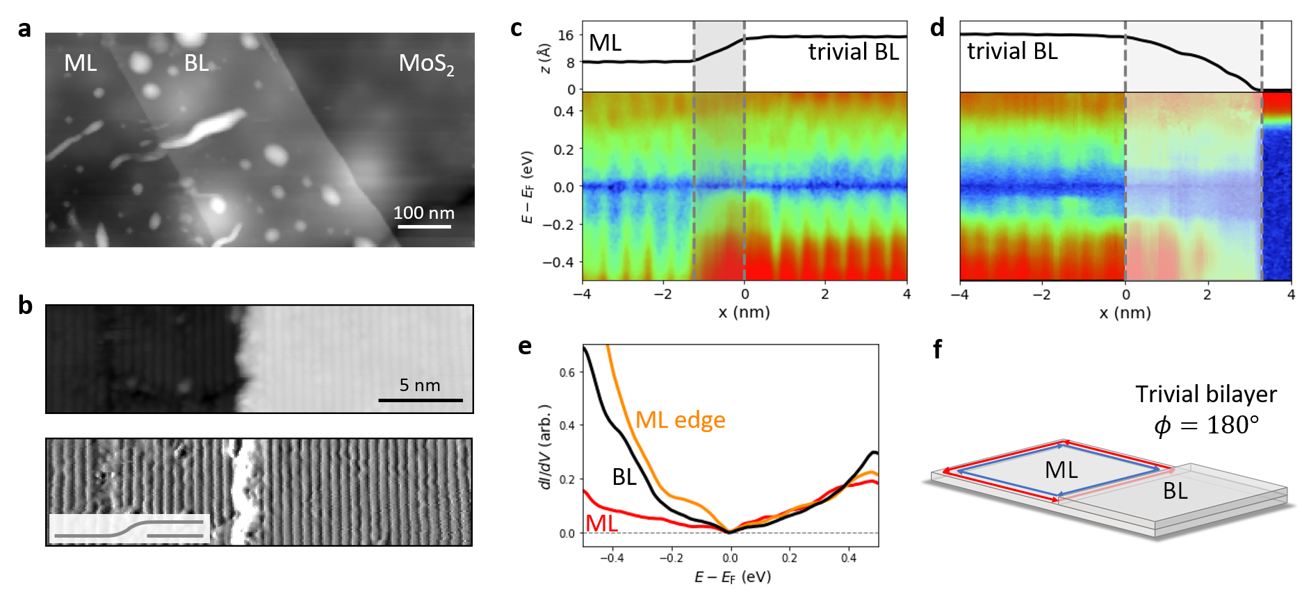
Next, we explore a step edge between a WTe2 monolayer and an as-grown topologically trivial bilayer (Fig. 3a, b). In the present sample, the top WTe2 layer of the as-grown bilayer is continuous and draped over the second layer underneath due to the flipping of the sample during fabrication. With multiple iterations of very carefully prepared sharp tips, we are able to resolve the draped monolayer free from significant tip artifacts and measure the tunneling conductance across the ML-BL junction (Fig. 3c and section S7). We find that there is a clear increase in the density of states in the WTe2 monolayer just before the bilayer, again with an extension of . The shape of this feature (Fig. 3c) shows remarkable agreement to that observed at the monolayer WTe2/MoS2 edge in Fig. 2d. We therefore conclude that the spectroscopic feature at the ML-BL junction is the manifestation of the QSH edge state between the topological WTe2 monolayer and the topologically trivial WTe2 bilayer (Fig. 3f). This finding verifies that there is a significant interlayer interaction in aligned, as-grown bilayer WTe2, which is in contrast to the above studied twisted bilayers. Such an interlayer-interaction-induced change in topology between the monolayer and bilayer is in agreement with WTe2 undergoing another topological phase transition at higher layer number, possibly to a higher-order topological insulator [12]. The corresponding edge states of bulk WTe2 have an electronic structure [27] that is distinctly different from the edge states observed in ML and tBL WTe2, indicating that these are in fact different topological states.
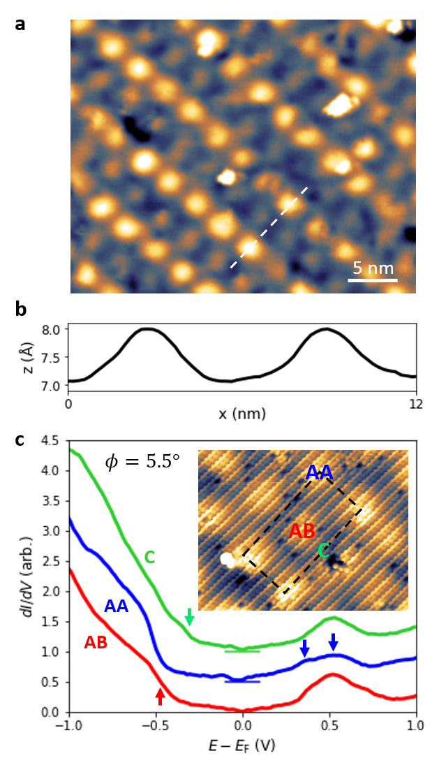
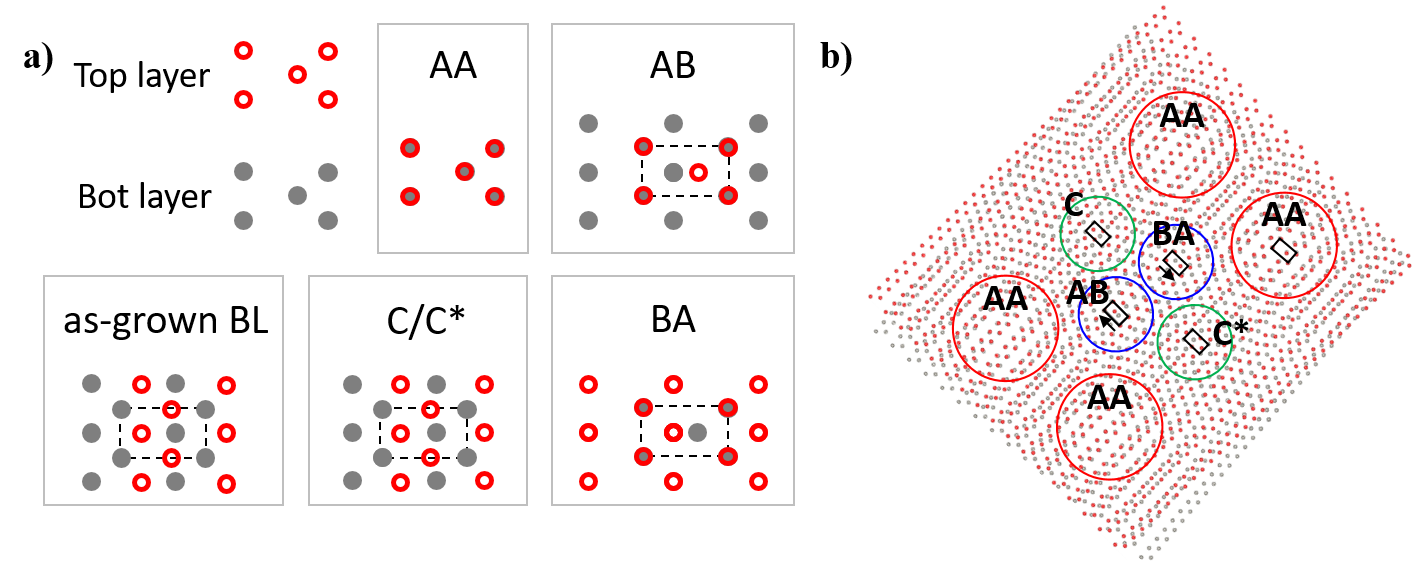
In order to analyze the effect of inter-layer interactions in greater detail, we further study a tBL sample which we fabricate using a modified tear-and-stack technique (for details see Materials and Methods and section S8). The tear-and-stack sample fabrication allows us to directly control the twist angle, and therefore manifest a moiré pattern in which the interlayer coupling is expected to be modulated across the moiré unit cell [22]. The resulting long-range moiré pattern has a rectangular unit cell and periodicity of nm (Fig. 4a, b). The corresponding twist angle is following the same angle definition as with the folded bilayer, which we also directly confirm at the tBL edge (Fig. S11). Resulting from the different stacking of W atoms, we observe two different corrugation maxima in the moiré unit cell, where the A-site W atom in one layer vertically aligns with the A- or B-site W atom of the other layer, i.e. AA- or AB-stacking, respectively. Due to the rectangular shape of the moiré unit cell, the AA-stacked sites form a distinct quasi-one-dimensional pattern, which has been proposed to result in an array of 1D Luttinger liquids at low energy [28].
Tunneling spectra recorded in different positions of the moiré unit cell (Fig. 4c) show distinctly different spectral features. In AA-stacked positions, the conduction band peak at shows a significant splitting, while spectra taken in AB sites show a stronger hybridization in the valence bands when compared to ML WTe2. Spectra taken at C stacked locations in the moiré unit cell show similarity to that of the as-grown bilayer, with a valence band feature at . Interestingly, this observation roughly coincides with the arrangement of W atoms in this location of the tBL moiré unit cell being similar to that of the as-grown bilayer, despite the C-stacked WTe2 having twist compared to the as-grown bilayer’s 180∘ (see section S8 and Fig. S12). Since this position also is the minimum of the moiré corrugation, we expect the hybridization of the two layers to be the strongest throughout the moiré unit cell. In combination, we attribute the distinct changes of the local electronic structure to the different interlayer interactions, which are the result of the local stacking geometry.
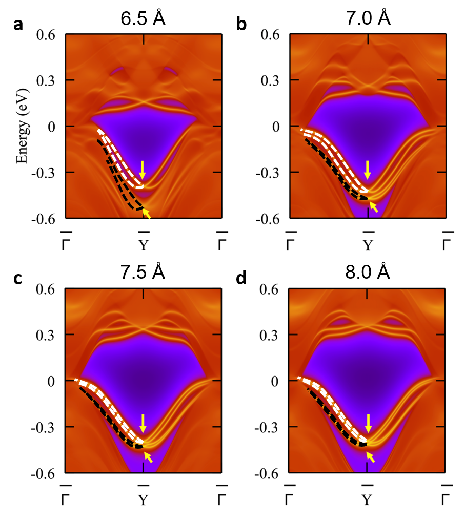
To understand the influence of interlayer distance and stacking on the electronic and topological properties of the WTe2 bilayers, we performed density functional theory (DFT) calculations of a WTe2 monolayer, trivial bilayer (), as well as a bilayer with , most closely resembling our experiments on small twist angle tBLs. In general, we find that weakly coupled WTe2 bilayers can be regarded as two decoupled monolayers, each retaining the electronic character of a WTe2 monolayer, i.e. the QSH state (). When bringing the layers closer together, they begin to interact and hybridize, leading to a global trivial topology, = 0, in agreement with our experiments and earlier studies [9]. The resulting charge transfer between the layers further leads to an increasing shift of their edge states with respect to each other (Fig. 5). We further investigate the effect of the subtle structural differences between the 1T’ and the 1Td phase on our calculations (see section S9) and find that the electronic and topological properties are strongly dependent on the stacking geometry owing to their different symmetries and interlayer spacings, which result in different amounts of charge transfer between the layers (Figs. S21 and S22). Interestingly, as we bring the bilayers very close together (Å in AA stacking), our calculations predict another topological transition back to = 1 for the Td phase (section S9 and Fig. S17). This interlayer distance is however significantly smaller than the Å realized in the AA location of our sample.
In summary, we conclude that it is possible to tune the topology of WTe2 bilayers via their twist angle and interlayer interactions. The discovered twist angle-dependent charge-transfer further makes tBL WTe2 a suitable system to probe the QSH edge-states of twisted bilayers in transport measurement since bulk conduction can be suppressed to not obscure the edge state transport.
Materials and Methods
Sample preparation
WTe2 and MoS2 were exfoliated onto SiO2/Si substrates. Cleaving WTe2 crystals produces flakes which have a high probability of producing edges that are aligned with one of the two crystal axes. We picked up a -thick MoS2 flake with a PPC/PDMS stamp and subsequently a WTe2 flake containing mono- and bilayer regions. After the WTe2 pickup, the heterostructure was flipped upside down and placed onto a gold lead on an SiO2 substrate which was pre-mounted and contacted to an STM sample plate. The tear-and-stack sample was fabricated in the same way, except that two pick-ups of the WTe2 took place with a slight rotation of the substrate after the first pickup. The exfoliation and stacking took place in a nitrogen-filled glovebox, from which the samples were transferred into a high vacuum tube furnace to remove the PPC by annealing at for . Subsequently, the samples are transferred into the STM ultra-high vacuum chamber where a final anneal at for () was performed, all sample transfers took place in nitrogen atmosphere.
STM measurements
STM measurements are performed using a commercial CreaTec setup with a sample stage temperature of . Electrochemically-etched tungsten tips were indented and checked for a clean spectrum on the gold leads prior and in between measurements. The measurements throughout the manuscript have been performed with multiple iterations of freshly prepared tip apices to exclude tip artifacts. measurements were performed using a lock-in amplifier set to a frequency of , at stabilization setpoint , and with a modulation amplitude , except for Fig. 1d and 4c, for which we used , , with a modulation amplitude
Acknowledgments
Funding: We acknowledge helpful discussions with Justin Song. P. G. would like to acknowledge fruitful discussions with Jaron T. Krogel and Yubo ‘Paul’ Yang. B.M.H. was supported by the Department of Energy under the Early Career award program (#DE-SC0018115). F.L. and D.W. were supported by the NSF DMR-1809145 for the STM measurements. The authors gratefully acknowledge NSF DMR-1626099 for acquisition of the STM instrument. F.L. was supported by the Center for Nanophase Materials Sciences, Oak Ridge National Laboratory, which is a DOE Office of Science User Facility. F.L. acknowledges funding from the Alexander von Humboldt foundation through a Feodor Lynen postdoctoral fellowship. F.L. further acknowledges funding by the Deutsche Forschungsgemeinschaft (DFG, German Research Foundation) within the Priority Programme SPP 2244 “2DMP” and the Bavarian Ministry of Economic Affairs, Regional Development and Energy within Bavaria’s High-Tech Agenda Project ”Bausteine für das Quantencomputing auf Basis topologischer Materialien mit experimentellen und theoretischen Ansätzen”. The authors thank the Pennsylvania State University Two-Dimensional Crystal Consortium - Materials Innovation Platform (2DCC-MIP), which is supported by NSF DMR-1539916 for supplying further 2D materials. While support for initial work by A.D.P. and P. G. was by the Oak Ridge National Laboratory’s Laboratory Directed Research and Development project (Project ID 7448, PI: P.G.), work on the key final results presented in the manuscript was supported by the U.S. Department of Energy, Office of Science, Basic Energy Sciences, Materials Sciences and Engineering Division, as part of the Computational Materials Sciences Program and Center for Predictive Simulation of Functional Materials. Computations were performed on the Compute and Data Environment for Science (CADES) cluster at the Oak Ridge National Laboratory, which is supported by the Office of Science of the U.S. Department of Energy under Contract No. DE-AC05-00OR22725, at the Center for Nanophase Materials Sciences, Oak Ridge National Laboratory, which is a DOE Office of Science User Facility. Crystal growth and characterization at ORNL was supported by the US Department of Energy, Office of Science, Basic Energy Sciences, Division of Materials Sciences and Engineering. Author contributions: F.L. and D.W. fabricated the samples, measured and analyzed the experimental data and wrote the manuscript. P.G. and A. D. P. performed the DFT calculations, interpreted the results and contributed to writing the manuscript. J.Y. and D.G.M. grew the WTe2 crystals. B.M.H. supervised the project. All authors commented on the manuscript. Competing interests: The authors declare that they have no competing interests. Data and materials availability: All data needed to evaluate the conclusions in the paper are present in the paper and/or the Supplementary Materials. Additional data related to this paper may be requested from the authors.
References
- [1] Geim, A. K. & Grigorieva, I. V. Van der Waals heterostructures. Nature 499, 419–425 (2013).
- [2] Qian, X., Liu, J., Fu, L. & Li, J. Quantum spin Hall effect in two-dimensional transition metal dichalcogenides. Science 346, 1344–1347 (2014).
- [3] Fei, Z. et al. Edge conduction in monolayer . Nat. Phys. 13, 677 (2017).
- [4] Tang, S. et al. Quantum spin Hall state in monolayer 1T’-WTe2. Nat. Phys. 13, 683 (2017).
- [5] Wu, S. et al. Observation of the quantum spin Hall effect up to 100 Kelvin in a monolayer crystal. Science 359, 76–79 (2018).
- [6] Shi, Y. et al. Imaging quantum spin Hall edges in monolayer . Sci. Adv. 5 (2019).
- [7] Sajadi, E. et al. Gate-induced superconductivity in a monolayer topological insulator. Science 362, 922 (2018).
- [8] Fatemi, V. et al. Electrically tunable low-density superconductivity in a monolayer topological insulator. Science 362, 926 (2018).
- [9] Muechler, L., Alexandradinata, A., Neupert, T. & Car, R. Topological nonsymmorphic metals from band inversion. Phys. Rev. X 6, 041069 (2016).
- [10] Fei, Z. et al. Ferroelectric switching of a two-dimensional metal. Nature 560, 336–339 (2018).
- [11] Li, P. et al. Evidence for topological type-II Weyl semimetal WTe2. Nat. Commun. 8, 2150 (2017).
- [12] Choi, Y.-B. et al. Evidence of higher-order topology in multilayer WTe2 from Josephson coupling through anisotropic hinge states. Nature Materials 19, 974–979 (2020).
- [13] Lüpke, F. et al. Proximity-induced superconducting gap in the quantum spin Hall edge state of monolayer WTe2. Nat. Phys. 16, 526–530 (2020).
- [14] Cao, Y. et al. Correlated insulator behaviour at half-filling in magic-angle graphene superlattices. Nature 556, 80–84 (2018).
- [15] Cao, Y. et al. Unconventional superconductivity in magic-angle graphene superlattices. Nature 556, 43–50 (2018).
- [16] Wang, L. et al. Correlated electronic phases in twisted bilayer transition metal dichalcogenides. Nature Materials 19, 861–866 (2020).
- [17] Yankowitz, M. et al. Tuning superconductivity in twisted bilayer graphene. Science 363, 1059–1064 (2019).
- [18] Lu, X. et al. Superconductors, orbital magnets and correlated states in magic-angle bilayer graphene. Nature 574, 653–657 (2019).
- [19] Wu, F., Lovorn, T., Tutuc, E., Martin, I. & MacDonald, A. H. Topological insulators in twisted transition metal dichalcogenide homobilayers. Phys. Rev. Lett. 122, 086402 (2019).
- [20] Pan, Y. et al. Quantum-confined electronic states arising from the moiré pattern of MoS2-WSe2 heterobilayers. Nano Lett. 18, 1849–1855 (2018).
- [21] Serlin, M. et al. Intrinsic quantized anomalous Hall effect in a moir heterostructure. Science 367, 900–903 (2020).
- [22] Waters, D. et al. Flat bands and mechanical deformation effects in the moiré superlattice of MoS2-WSe2 heterobilayers. ACS Nano (2020).
- [23] Kane, C. L. & Mele, E. J. Quantum spin hall effect in graphene. Phys. Rev. Lett. 95, 226801 (2005).
- [24] Jia, Z.-Y. et al. Direct visualization of a two-dimensional topological insulator in the single-layer 1T’-WTe2. Phys. Rev. B 96, 041108 (2017).
- [25] Arora, A., Shi, L.-k. & Song, J. C. W. Cooperative orbital moments and edge magnetoresistance in monolayer . Phys. Rev. B 102, 161402 (2020).
- [26] Zhao, W. et al. Determination of the spin axis in quantum spin hall insulator monolayer WTe2. arXiv:2010.09986 (2021).
- [27] Peng, L. et al. Observation of topological states residing at step edges of . Nat. Commun. 8, 659 (2017).
- [28] Wang, P. et al. One-dimensional luttinger liquids in a two-dimensional moiré lattice. arXiv:2109.04637 (2021).
Supplementary Information: Quantum spin Hall edge states and interlayer coupling in twisted-bilayer WTe2
Felix Lüpke1,2,3,4, Dacen Waters1,5, Anh D. Pham2, Jiaqiang Yan6,
David G. Mandrus,3,6,7, Panchapakesan Ganesh2, Benjamin M. Hunt1,†
1Department of Physics, Carnegie Mellon University, Pittsburgh, PA 15213, USA
2Center for Nanophase Materials Sciences, Oak Ridge National Laboratory,
Oak Ridge, TN 37831, USA
3Department of Materials Science and Engineering, University of Tennessee, Knoxville, TN 37996, USA
4Peter Grünberg Institut (PGI-3), Forschungszentrum Jülich, 52425 Jülich, Germany
5Department of Physics, University of Washington, Seattle, WA 98195, USA
6Materials Science and Technology Division, Oak Ridge National Laboratory,
Oak Ridge, TN 37831, USA
7Department of Physics and Astronomy, University of Tennessee, Knoxville, TN 37996, USA
† E-mail: bmhunt@andrew.cmu.edu
S1 Folded bilayer sample
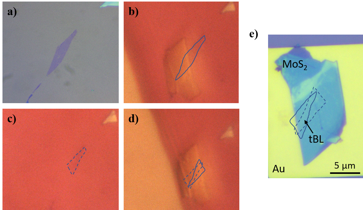
Data shown in Figs. 1 and 2 of the main text was taken in different regions of the same WTe2/MoS2 heterostructure (sample #1). This heterostructure was fabricated using the dry-transfer flip technique reported in Ref. [1]. Flakes are exfoliated from bulk MoS2 and WTe2, which was characterized to be in the 1T’ phase, onto 285 nm SiO2. After exfoliation, the MoS2 flake is picked up with a PPC/PDMS stamp, followed by the WTe2 flake. Subsequently, the heterostructure is flipped upside down and then placed on a Cr/Pd/Au lead which was pre-evaporated on SiO2 using optical lithography and is connected to a contact of the STM sample plate. The sample is then transferred to a vacuum annealer () and annealed over night. From there, the sample is transferred back to the glovebox to take optical images and then to the STM chamber. For all transfers, the sample is always in a nitrogen atmosphere and never exposed to air. The sample fabrication took less than starting from exfoliation in the nitrogen-filled glove box (O2, H2O ). In our experience, the MoS2 thickness has to be in order to be able to tunnel on it at , because otherwise it is too insulating. Optical images of the exfoliated WTe2 flake on SiO2 and of the assembled heterostructure are shown in Fig. S1.
S2 Crystal symmetry and folded/twisted bilayer comparison
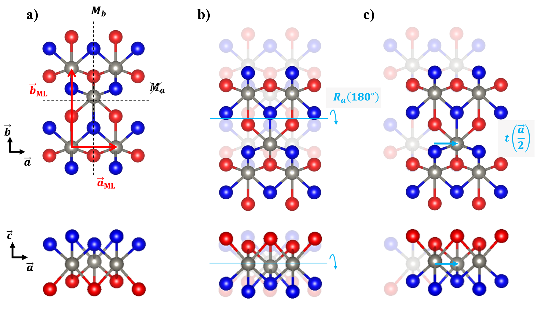
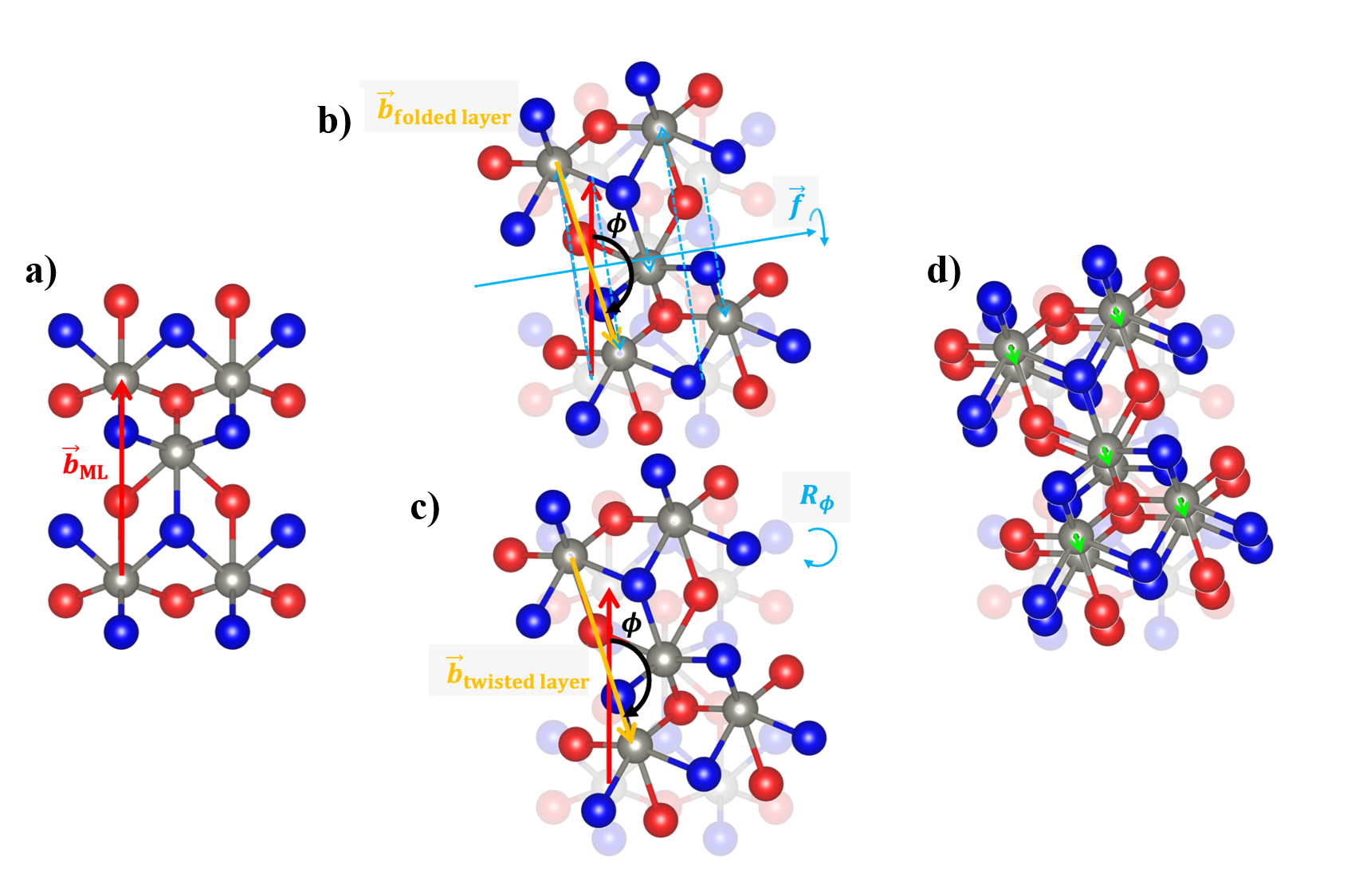
1T’-WTe2 has a screw-axis symmetry along the -axis, i.e. . The screw transformation is demonstrated stepwise in Fig. S2. Rotation about the -axis by and a translation by half a unit cell along the -axis returns the original unit cell. The screw operation resembles a fold, as in the folded bilayers presented in the main text. As a result of the symmetry, a folded layer bilayer can be considered equivalent to a twisted bilayer, as demonstrated in Fig. S3. Folding along an arbitrary axis (i.e. a rotation about that axis, as shown in Fig. S3b) results in a rotation between the folded unit cell vectors and the original unit cell vectors. Similarly, by just rotating about the -axis (as in Fig. S3c), the same twist angle can be obtained. It follows that the two scenarios are equivalent, modulo an arbitrary lateral translation (Fig. S3d).
S3 Summary of tunneling spectra
Tunneling spectra in the range acquired on the different regions of the WTe2 flake of sample #1 are shown in Fig. S4. In as-grown bilayer WTe2, the hybridization of the two layers leads to a semi-metallic state which is evident in the spectra as an increased density of states especially on the valence band side. This increase is mostly absent in the folded bilayers.
S4 Additional folded bilayers
We have analyzed another folded region of sample #1 which has two domains, separated by a lateral domain boundary (Fig. S5a). From atomic resolution scans of the two different domains (Fig. S5b and c), we find that and , respectively. Tunneling conductance measurements across the edge of the two additional tBL regions (Fig. S5d and e) show similar results as in Fig. 2 of the main text. While unsurprising for the large twist angle of , for it is somewhat suprising that the electronic structure in this domain still represents that of a decoupled monolayer (for spectra in range see Fig. S4), as in other tBL TMDs or graphene, highly correlated phenomena are reported at similar twist angles [2, 3]. We explain this observation by the fact that an important aspect of the correlated phenomena in magic-angle bilayers are flat bands which are formed due to the periodicity of the resulting moiré pattern. However, for we estimate the WTe2 moiré pattern periodicity to be , where and the lattice mismatch , i.e. comparable to the size of the entire domain. We therefore conclude that moiré effects do not play a role in this domain despite the small twist angle. We have further performed tunneling conductance measurements across the lateral domain boundary which agree well with domain boundaries in epitaxially grown 1T’-WSe2 monolayers [4] as discussed below.
S5 Topologically trivial domain boundary state
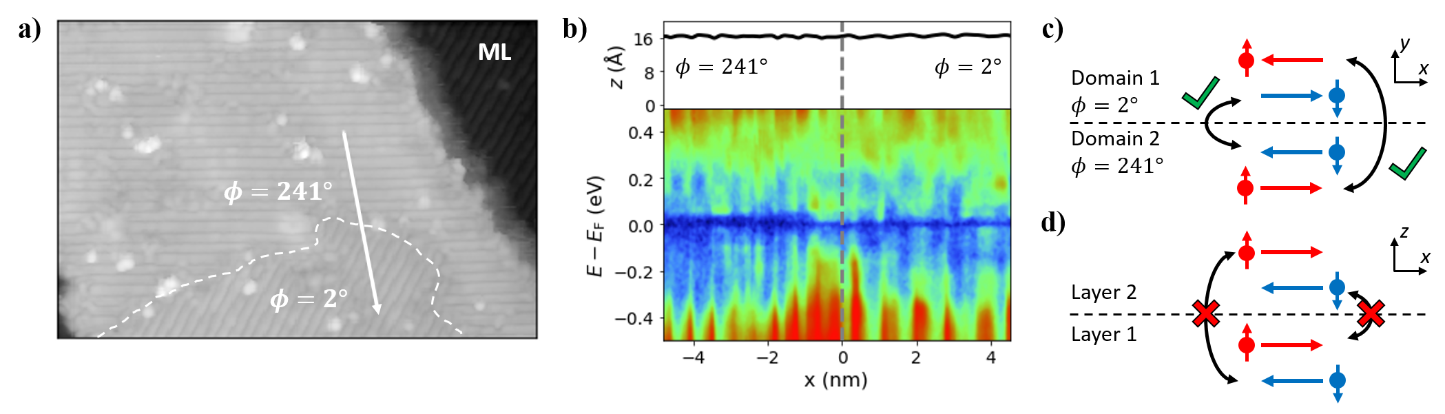
Figure S6a shows a zoom into the domain boundary on the folded WTe2 layer shown in Fig. S6. The relative crystallographic orientation between the two domains corresponds to withing measurement error (Fig. S6a). While the observation of domain boundaries in exfoliated flakes is rare in our experience, the domain boundary was reported in epitaxially grown 1T’-WSe2 as the most common configuration [4]. While detailed measurements at the domain boundary are difficult because of its irregular shape and many defects along the boundary, Fig. S6b shows a tunneling conductance measurement across the domain boundary in which we observe an increased density of states at the position of the domain boundary, similar to that of the QSH edge state feature. This observation is in agreement with the presence of two instances of counter-propagating QSH edge states, one on each side of the domain boundary. However, in this configuration backscattering from one QSH channel into the other is possible (Fig. S6c) and the channels hybridize. This is in contrast to the configuration of two QSH edge states sitting on top of each other in the folded bilayers as shown Fig. 2 of the main text. The observation of counter-propagating QSH states at the domain boundary supports our conclusion that both, the and domain, are topologically non-trivial. These observations are consistent with previous work on domain boundary states in epitaxially grown 1T’-WSe2 [4].
S6 Edge detection scheme
To identify the positions of the topographic edges, we use an edge detection scheme based on the topography gradient. We apply this scheme to each edge separately, but using the same criteria to achieve an edge detection that does not require subjective inputs for each data set. To detect the edge positions, we determine a threshold for the topography gradient of after applying a moving average filter to achieve a robust detection. Approaching an edge, the position of the edge is determined as the position where reaches this threshold. Figs. S7 and S8 show the edge detection for the data sets analyzed in the main paper as well as Fig. S5, with the respective threshold values indicated as horizontal dotted lines, as well as the corresponding signal at .
S7 Exclusion of tip artifacts at ML-BL junction
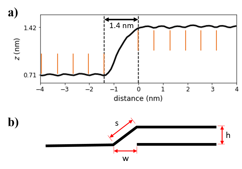
To confirm the measurement of the continuous WTe2 layer draped over a second layer below without artifacts, we carefully analyze the lateral position of the atomic rows across the step edge (Fig. S9a). We find that the transition region corresponds to three WTe2 unit cells which corresponds to a length of .
In combination with the observed step height of Å, this allows us to estimate the width of the transition region to be (Fig. S9b). While this value is slightly greater than the experimentally observed transition region () we attribute this difference to the ’s’ shape of the transition region which results in a smaller lateral extension compared to our simple model.
However, more importantly, we take the fact that the observed transition region is less extended than the estimated size as evidence that there are no significant tip artifacts due to a blunt tip, as this would extend the transition region.
Furthermore, we observe a small modulation of the profile throughout the transition region which corresponds to the expected atomic rows, also supporting the absence of any significant tip artifacts in this measurement.
We note that while there are dangling bonds at the ML-BL junction, they are located underneath the ML and therefore not expected to significantly contribute to the measured tunneling conductance in the top layer of the the ML-BL transition region.
S8 Tear-and-stack bilayer sample
The tear-and-stack tBL WTe2 heterostructure (sample #2) was fabricated utilizing an MoS2 substrate flake by first picking up only a portion of the WTe2 flake. The substrate + ML WTe2 portion was then translated laterally, rotated by a small angle, and aligned to the remaining ML WTe2 resulting in a overlap region of about 500 nm width. The height difference between the two layers is estimated at the edge of the tBL region to be Å on average (Fig. S11c). At the same edge, we observe an edge state similar to that of a WTe2 ML and the folded bilayer sample. Atomic resolution images from the ML WTe2 region indicate that the twist angle is about . Since the moiré wavelength is not isotropic, we must consider what interference gives rise to the moiré pattern, and keep in mind directionality. The direction of the moiré wavelength can be understood in the context of a beat frequency in real space, formed due to the difference of wavevectors . Considering the long-axis of the ML WTe2 unit cell as an example (i.e. the real space lattice vector ), we find that for a small twist angle , the difference in wave vectors gives . For small angles, this is such that the direction of associated with the long-axis moiré pattern is along the direction. The same logic can be applied to the smaller axis (-axis) of the rectangular ML WTe2 unit cell. Therefore, one would expect that there should be a moiré pattern perpendicular to the long axis of the ML WTe2 unit cell of wavelength and a shorter moiré pattern perpendicular to the short of axis of the WTe2 unit cell of wavelength . The moiré wavelengths are found to be and , and the directionality can be seen to align well with our prediction that the long (short) moiré wavelength is perpendicular to the long (short) axis of the WTe2 unit cell (main text, Fig. 5). The angle determined from the moiré wavelengths are then and , respectively, in excellent agreement with the atomic resolution images.
To understand the moiré domains, it is helpful to consider only the metal atoms of the ML WTe2 unit cell and that the two layers are rigid lattices (i.e. no relaxation effects [5]). This is likely a good approximation since the twist angle is relatively large and relaxation effects are not expected to play a significant role. Schematics of a few high-symmetry points in the moiré pattern between the rotated rigid lattices are shown in Fig. S12a. When AA-stacked, all of the W atoms line up, while AB stacking results in one of the W atoms from the top layers covering the other W atom from the bottom layer (and vice versa for BA stacking).
A diagram of the moiré pattern formed from the two layers is shown in Fig. S12b.
In this picture, AB and BA stacked regions are very close together in the center of the rectangular moiré unit cell, which might explain why there are not separate domains in STM topography, as evident in Fig. 4 of the main text. The absolute corrugation maxima are likely associated with AA stacking and the second corrugation maxima are associated with the AB and BA stackings. Without relaxation, any topological or spectral differences must be associated with local stacking registries and some small height difference effects due to energetically preferred interlayer distances.
A comparison of the tunneling spectra acquired in the different moiré registries is shown in Fig. S13.
The tear-and-stack fabrication method of this sample caused a relatively discorded edge, limiting the high-quality spectral analysis across the edge state. We include an example line spectra across the edge, indicating a spectral feature similar to the QSH edge state reported in the main text. While overall consistent with our interpretations in the main text, it is difficult to conclude the influence of moiré pattern on the QSH state due to lack of theoretical predictions as function of twist angle and requirement of higher-quality and smaller-angle devices.
S9 DFT calculations
| Structure | Spacegroup |
|---|---|
| Monolayer T’ | P21/m (11) |
| AA-stacked bilayer T’ | P21/m (11) |
| As-grown bilayer T’ | Pm (6) |
| Monolayer Td | Pm (6) |
| AA-stacked bilayer Td | Pm (6) |
| As-grown bilayer Td | Pm (6) |
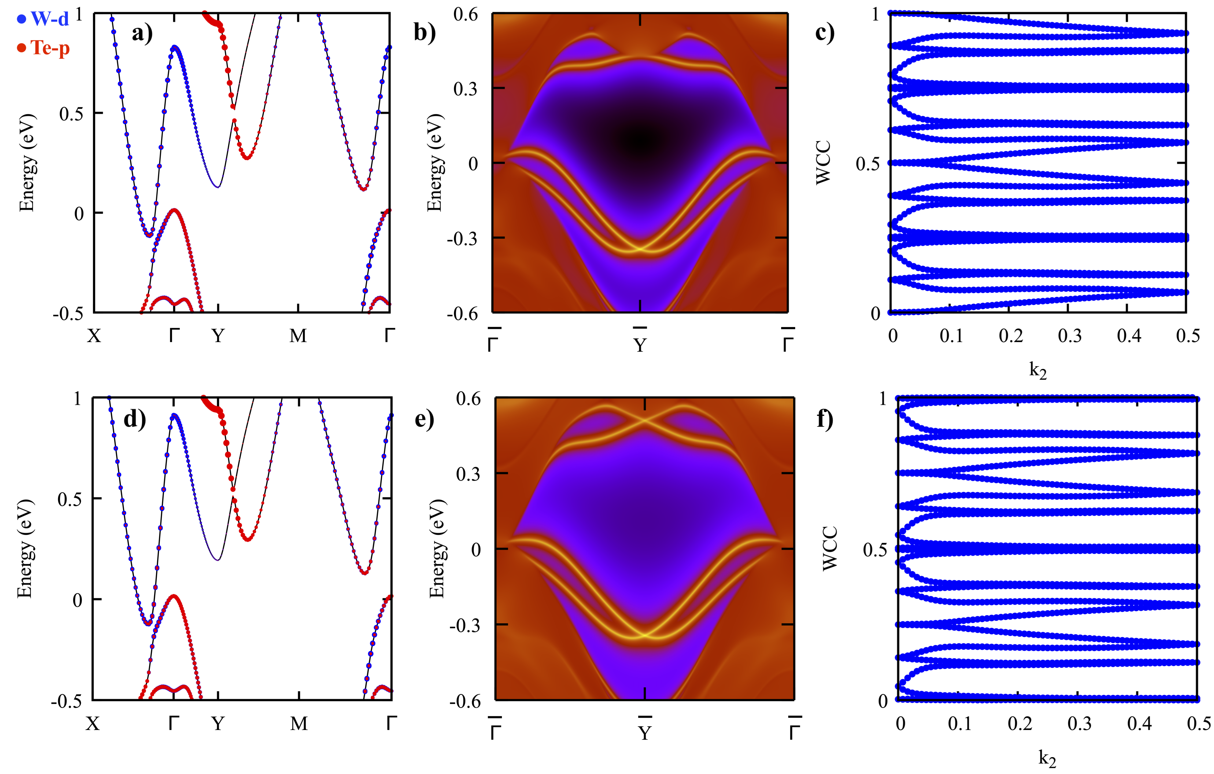
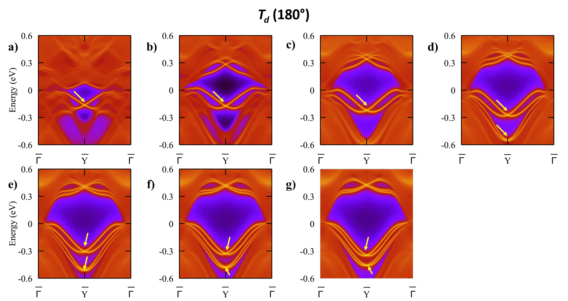
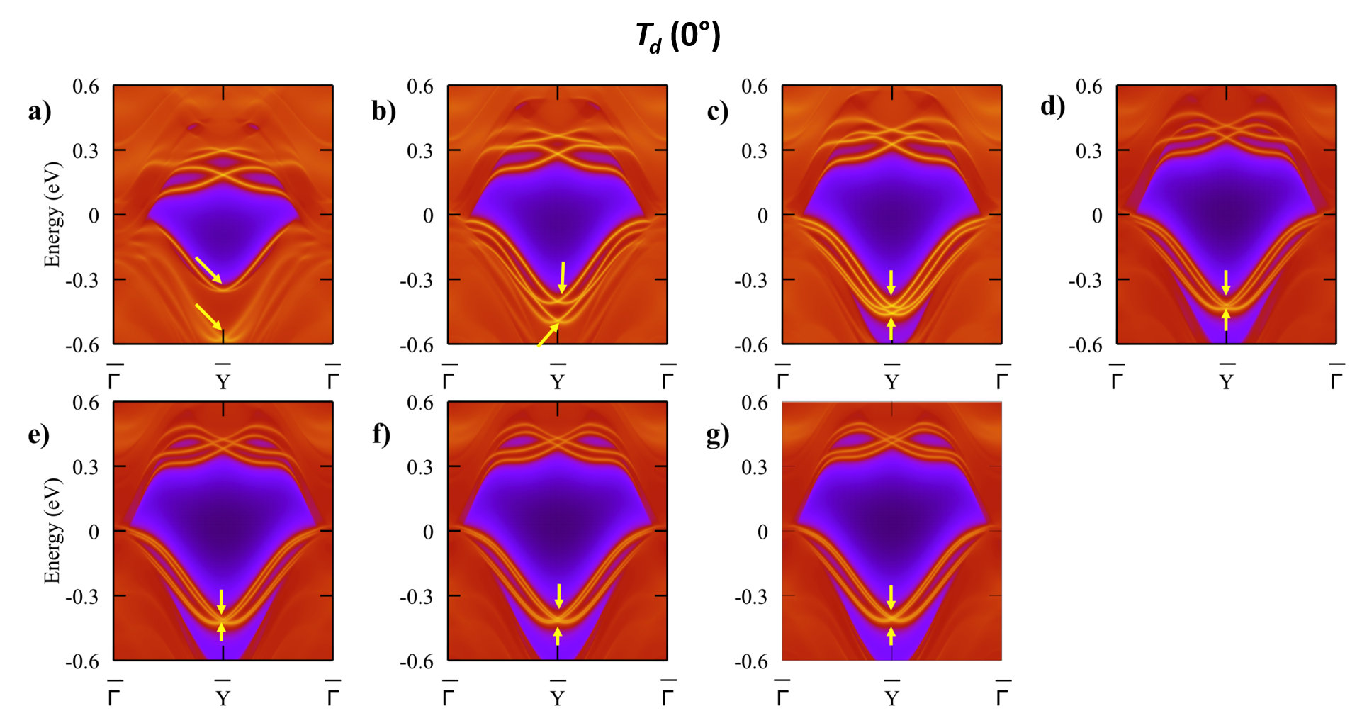
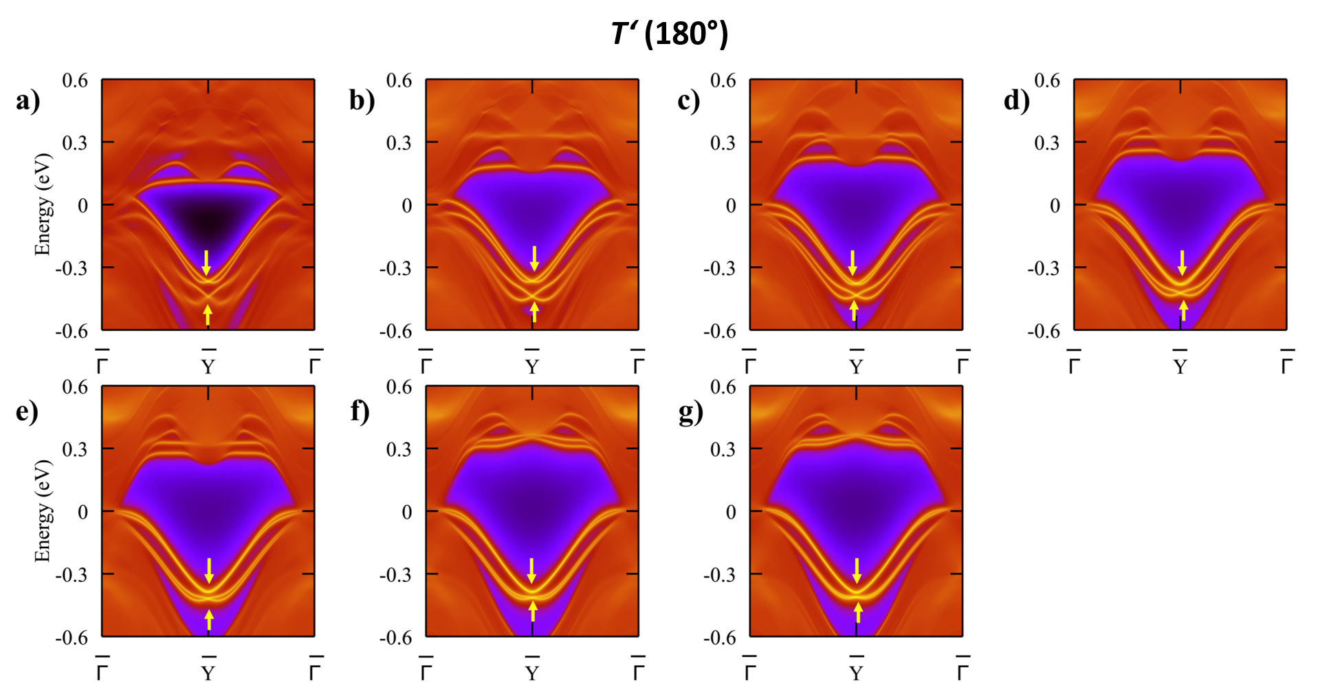
DFT calculations were performed using the VASP PAW potentials [6, 7], and van der Waals (vdW) functional opt86b [8, 9], an energy cut off of 260 eV and a dense centered 12101 k-mesh. For our structures, we consider the monolayer and bilayer configurations in the T’ (Fig. S14) and Td (Fig. S15) phases. In all calculations, the lattice parameters for the monolayer and bilayer structures were set at Å and Å. In our notation, the Td phase corresponds to an orthorhombic spacegroup Pmn21 (space group 31) with in the bulk, and the T’ phase belongs to the monoclinic spacegroup P21/m (space group 11) with a small tilt angle and , similar to Ref. 10. To meet our definition of the a lattice vector in the main text to be shorter than the b lattice vetor, we rotate the structure by 90∘, resulting in ∘ and ∘ in the T’ phase. A vacuum gap of Å was applied to all the configurations. For bilayer configurations, we consider the as-grown bilayer as well as bilayer for both, Td and T’ structures. A summary of the structural symmetries for the monolayer and bilayer with different stacking is shown in table S1. In addition, for the different stacking in the Td and T’ phase, we vary the interlayer distance in steps of Å to study its effect on interlayer interaction, charge transfer and topology. The interlayer distance is defined as the distance between the W atoms in top and bottom layers. Effects of relaxation were not found to change the topology, which is preserved by the overall symmetry. As such, we only report results for the case where internal coordinates are unrelaxed. The topology and edge states were calculated using the WannierTools program [11] based on projecting a tight-binding Hamiltonian for the low-energy bands around the Fermi-level onto W d orbitals and Te p orbitals using the Wannier90 package [12]. The charge transfer effect was investigated using the Bader analysis [13] with the charge difference = - - .
The effect of charge transfer is calculated to be strongest in the as-grown Td bilayer. The charge transfer in tBL Td is smaller than in the corresponding T’ tBL bilayer. In AA-stacked T’ tBL, the charge transfer effect is completely absent. In the as-grown T’ bilayers, there is a strong charge transfer between the layers, due to the lack of inversion symmetry, resulting in a polar metal. This is in stark contrast to the AA-stacking where the inversion symmetry is preserved, indicating weak coupling between the layers. In the Td phase, a charge transfer is present in both of the AA and as-grown bilayer due to their common lack of inversion symmetry, which also indicates the existence of the polar metal state in these configuration. However, in the as-grown Td bilayer a much stronger charge transfer effect is observed, indicating strong coupling between the layers. In contrast, the stacking results in a significantly smaller charge transfer, thus suggesting a weaker interlayer coupling.
Based on our calculation, ML WTe2 in the Td and T’ phase are topologically non-trivial with = 1 even though they belong to different symmetry classes (table S1). As a result, they both exhibit a topological edge state when cutting along the -axis (Fig. S16). Based on our DFT calculations, the edge states for, both, monolayer Td and T’ are mostly located in the valence bands, similar to previous theoretical study of the edge state in 1T’ monolayers [14]. In addition, the prediction of the non-trivial in ML WTe2 in the Td phase is also consistent with recent model Hamiltonian prediction [15].
For the bilayer configurations in the Td and T’ phases, we find the stacking geometry and interlayer distance to be important factors to determine the topology and charge transfer between the layers. In the Td phase, the topology of the as-grown bilayer undergoes a transition from a = 1 to = 0 when we change the layer distances from being far apart to being extremely close together (Fig. S17). In contrast, in the AA-stacked Td bilayer globally regardless of the interlayer distance. Nevertheless, the electronic structure of the edge states varies significantly as function of interlayer distance. As shown in Fig. S17, the edge state in the as-grown Td bilayer forms a single band when the layers are close, which transition to two edge bands at a critical interlayer distance of Å. This is in agreement with the observed topological transition. The position of the two edge states remains largely unchanged above the critical interlayer distance of Å. In the AA-stacked Td bilayers, the global invariant is equal to zero, but the two edges show a strong hybridization as the layers move further apart S18. In addition, because of the inversion symmetry breaking in both stacking configurations in the Td phase (table S1), the charge transfer effect is predicted to exist in the as-grown and AA-stacking, however the strength of this effect is shown to be reduced in the AA-stacking (Fig. S21).
In the T’ phase, the inversion symmetry is preserved in the AA-stacking, thus a charge transfer only occurs in the as-grown bilayer (Fig. S22). In addition, even though there is no topological transition happening in the as-grown T’ bilayer as function of interlayer distance, the edge states also exhibit similar behavior as the Td phase when the two layers are further apart. Specifically, in the AA-stacking, the two layers’ edge states hybridize (Fig. S20) as the two layers are further apart while the edge states in the as-grown bilayer are largely unaffected with respect to the different interlayer distance.
In our experiments, even though we can not distinguish between the Td and T’ phases for the different bilayers, our DFT calculations suggest that only the stacking geometry and the interlayer distance are important in determining the topology and the charge transfer. Specifically, the AA-stacking in both of the Td and T’ phase shows a significantly reduced charge transfer effect in comparison to the as-grown bilayers, thus suggesting a less metallic behavior in the AA-stacking bilayers compared to the as-grown structures regardless of the crystal symmetries. This DFT prediction is consistent with the experimental observation of an overall smaller dI/dV signal in the twisted bilayer compared to the as-grown bilayer (compare Fig. 2 and 4 of the main text). In addition, the charge transfer for the AA-stacking is shown to be diminished significantly in our DFT calculation in both of the Td and T’ phases. Experimentally, we observe the interlayer distance in the twisted BL to be larger than for the as-grown BL which supports the absence of a significant charge transfer in the measured tBL.
In addition to the reduced charge transfer in the AA-stacking, our DFT calculations also predict a strong hybridization between the edge states on the individual layers when the interlayer separation distance is large in the AA-configuration for both Td and T’ phases. As a result, since the interlayer distance is large for the tBL as measured in our experiments, the QSH edge-states can appear as the sum over the two layers as shown in Fig. S18 and Fig. S20 . Specifically, the overall topology of the tBL can be considered as a system of two stacked strong topological insulators due to the weak interlayer coupling, resulting from a large interlayer distance and twist angle rotation. Consequently, such a system can posses a unique four-fold Dirac point due to the overlapping of the individual Dirac points located on the two different layers (Fig. S18 and Fig. S20). As a result, in scanning tunneling experiments of tBL’s (with small rotational misalignement) the edge states are expected to be similar to that of the ML in agreement with Figs. 2e and f in the main text.
References
- [1] Lüpke, F. et al. Proximity-induced superconducting gap in the quantum spin Hall edge state of monolayer WTe2. Nat. Phys. 16, 526–530 (2020).
- [2] Cao, Y. et al. Unconventional superconductivity in magic-angle graphene superlattices. Nature 556, 43–50 (2018).
- [3] Wang, L. et al. Correlated electronic phases in twisted bilayer transition metal dichalcogenides. Nature Materials 19, 861–866 (2020).
- [4] Pedramrazi, Z. et al. Manipulating topological domain boundaries in the single-layer quantum spin Hall insulator 1T’-WSe2. Nano Lett. 19, 5634–5639 (2019).
- [5] Waters, D. et al. Flat bands and mechanical deformation effects in the moiré superlattice of MoS2-WSe2 heterobilayers. ACS Nano (2020).
- [6] Blöchl, P. E. Projector augmented-wave method. Phys. Rev. B 50, 17953–17979 (1994).
- [7] Hobbs, D., Kresse, G. & Hafner, J. Fully unconstrained noncollinear magnetism within the projector augmented-wave method. Phys. Rev. B 62, 11556–11570 (2000).
- [8] Lee, K., Murray, E. D., Kong, L., Lundqvist, B. I. & Langreth, D. C. Higher-accuracy van der waals density functional. Phys. Rev. B 82, 081101 (2010).
- [9] Klimeš, J. c. v., Bowler, D. R. & Michaelides, A. Van der waals density functionals applied to solids. Phys. Rev. B 83, 195131 (2011).
- [10] Xu, S.-Y. et al. Electrically switchable berry curvature dipole in the monolayer topological insulator WTe2. Nat. Phys. 14, 900 (2018).
- [11] Wu, Q., Zhang, S., Song, H.-F., Troyer, M. & Soluyanov, A. A. Wanniertools: An open-source software package for novel topological materials. Comput. Phys. Commun. 224, 405 – 416 (2018).
- [12] Mostofi, A. A. et al. wannier90: A tool for obtaining maximally-localised wannier functions. Comput. Phys. Commun. 178, 685 – 699 (2008).
- [13] Tang, W., Sanville, E. & Henkelman, G. A grid-based bader analysis algorithm without lattice bias. Journal of Physics: Condensed Matter 21, 084204 (2009).
- [14] Lau, A., Ray, R., Varjas, D. & Akhmerov, A. R. Influence of lattice termination on the edge states of the quantum spin hall insulator monolayer . Phys. Rev. Materials 3, 054206 (2019).
- [15] Garcia, J. H. et al. Canted persistent spin texture and quantum spin hall effect in . Phys. Rev. Lett. 125, 256603 (2020).