Effect of deep-defect excitation on mechanical energy dissipation of single-crystal diamond
Abstract
The ultra-wide bandgap of diamond distinguished it from other semiconductors, in that all known defects have deep energy levels that are inactive at room temperature. Here, we present the effect of deep defects on the mechanical energy dissipation of single-crystal diamond experimentally and theoretically up to 973 K. Energy dissipation is found to increase with temperature and exhibits local maxima due to the interaction between phonons and the deep defects activated at specific temperatures. A two-level model with deep energies is proposed to well explain the energy dissipation at elevated temperatures. It is evident that the removal of boron impurities can substantially increase the quality factor of room-temperature diamond mechanical resonators. The deep-energy nature of nitrogen bestows single-crystal diamond with outstanding low-intrinsic energy dissipation in mechanical resonators at room temperature or above.
pacs:
62.40.+i, 61.72.-y, 65.40.-bRecent developments in micro-electromechanical system (MEMS) and nano-electromechanical system (NEMS) resonators have created opportunities for ultrasensitive sensors for mass Chaste et al. (2012); Sage et al. (2015, 2018), force Tang et al. (2019); El Mansouri et al. (2019), single molecule Hanay et al. (2012); Puller et al. (2013), and quantum spin detection Rugar et al. (2004); Barson et al. (2017). Among the many materials for MEMS/NEMS, diamond has attracted intense interest owing to its excellent mechanical properties and high-temperature stability Williams (2011); Najar et al. (2014); Khanaliloo et al. (2015); Regan et al. (2020); McSkimin and Andreatch (1972). In particular, the coupling of mechanical resonators with nitrogen-vacancy presents a promising vision for quantum sensing Ovartchaiyapong et al. (2014); Li et al. (2016). Resonators with high frequency and high quality factor () are in demand for precise measurement and quantum control. Diamond mechanical resonators have been reported with resonance frequencies above the gigahertz range Gaidarzhy et al. (2007) and factors as high as Tao et al. (2014). Dissipative mechanisms, such as clamping losses, multiple-material dissipation, surface losses, thermoelastic dissipation (TED), mechanical defects (MD), and quantum dissipation, can determine the factor of a mechanical resonator. With regard to intrinsic energy dissipation, in addition to TED, defects are also expected to determine the ultimate factors of the resonators.
For narrow-bandgap semiconductors, dopants can be fully ionized at room temperature (RT), reducing the factors even below RT Mohanty et al. (2002); Houston et al. (2002); Gysin et al. (2004). Diamond has an ultra wide bandgap (UWBG) of 5.5 eV. Defects in diamond usually have deep energy natures Sohn et al. (2015); Goss et al. (1996); Jones et al. (1996), which are less active at room temperature. To date, there have been no reports on the effect of deep defects on the energy dissipation of diamond. An understanding of these effects is required for enhancing ultimate device performance.
In this Letter, the energy dissipation in single-crystal diamond (SCD) mechanical resonators was investigated from RT to 973 K. It is revealed that the factors overall decrease with increasing temperature. However, two peaks appear near 400 K and 900 K. A two-level model is proposed to explain the factors at high temperatures. The defects corresponding to the factors at 400 K and 900 K have deep ionization energies near 0.3 eV and 0.9 eV, respectively. From this result, we speculate that single-crystal diamond is an ideal candidate for intrinsically high factor mechanical resonators, because the only unintentional nitrogen defect is inactive at RT. This observation is contrary to semiconductor devices, in which shallow dopants are needed for enough carriers but induce mechanical dissipation, and deep defects have the negative effect of reducing electron mobility Sze (2008); Romero et al. (2020).
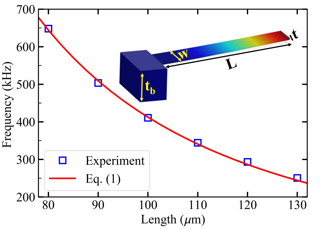
The SCD cantilevers were fabricated by a smart-cut method as described in Liao et al. (2010); Zhang et al. (2019), which has the structure of SCD-on-SCD. The SCD cantilevers of diamond sample 1 (DS1) were processed in oxygen ambient at 773 K to remove the ion-irradiated defects at the bottom of the cantilevers Wu et al. (2018). The dimensions of the cantilevers are as follows: thickness m and length from m to m, and width of 6 and 12 m. The inset in Fig. 1 shows a schematic of an SCD cantilever. To obtain the resonance frequency spectra, the SCD cantilevers were actuated by a radio-frequency signal applied to a probe placed aside the SCD cantilevers. The out-of-plane resonance frequencies of the cantilevers were detected with a laser Doppler vibrometer Zhang et al. (2019). The samples were measured in a high vacuum with a pressure of approximately Pa to eliminate air damping. The measurements were conducted from RT to 1000 K in steps of 25 K, which was controlled by a Lake Shore Model 335 temperature controller. To exclude the effect of the surface adsorbates on the resonance frequencies and factors, the SCD cantilevers were annealed at 1000 K for 1 h before the detailed measurements (Fig. S1) Sup . The factor is calculated as . The measured resonance frequency spectra were fitted on the basis of the Lorentzian line shape (Fig. S2) Christopoulos et al. (2019); Born and Wolf (2013); Sup . Here, is the resonance frequency and is the full width at half maximum (FWHM) of the resonance peak. To preclude the effect of thermal drift on the factors, we measured the frequency spectra back and forth, until there was no change in the resonance peak.
First, the length-dependent resonance frequencies of the SCD cantilevers were utilized to rule out the stress effect on the resonance frequency and factors Verbridge et al. (2006). We confirmed that the out-of-plane resonance frequency of the cantilevers can be described in the following form Weaver Jr et al. (1990), as shown in Fig. 1:
| (1) |
where is the vibration mode index, with , and and are the length and thickness of the cantilever, respectively. For SCD, the Young’s modulus GPa and the density of mass at RT. In addition, we fit the length-dependent resonance frequency by considering the stress in the cantilevers by Burek et al. (2013); Ikehara et al. (2000)
| (2) |
where is the magnitude of the uniaxial compressive stress along the length of the beam, is the bending moment, and is the cross-sectional area. It is shown in Table S1 that the stress in the SCD cantilevers is negligible Sup .
Second, we investigated the temperature-dependent resonance frequency to extract the Young’s modulus as a function of temperature for subsequent energy dissipation analysis. The resonance frequency of the SCD cantilevers (III-4 and IV-3 of sample DS1) as a function of temperature is shown in Fig. 2. The exponential decrease in the experimental resonance frequency with temperature is modeled by the temperature-dependent Young’s modulus Wachtman et al. (1961):
| (3) |
where is the Young’s modulus at 0 K. is a constant independent of temperature, and is a characteristic temperature related to the SCD Debye temperature with . Anderson theoretically obtained a similar formula based on the change in specific heat with temperature Anderson (1966). The fitting result of the resonance frequency with temperature is shown by the solid lines in Fig. 2, where the fitting was conducted by combining Eqs. (1)-(3), the parameters for the fittings are listed in Table 1. The variation in resonance frequency with temperature further confirms the negligible stress in the cantilevers. A similar tendency of resonance frequency temperature was also observed for other cantilevers, as shown in Fig. S3(a) and Fig. S4 Sup .
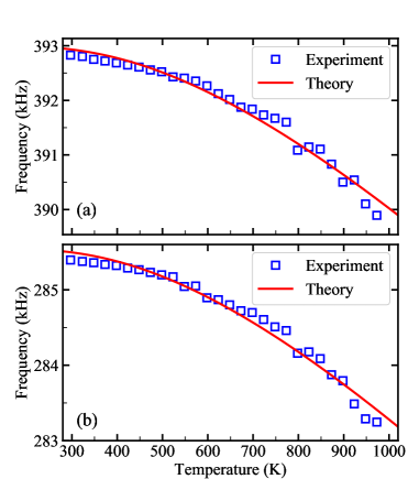
| Length | Width | |||
| Sample 1 | (m) | (m) | (MPa) | (MPa) |
| III-4 | 100 | 12 | 45.16 | 6.14 |
| IV-3 | 120 | 12 | 51.79 | 0.27 |
The quality factor is defined as the ratio of the stored energy in the resonator to the dissipated energy per cycle of vibration Pozar (2009); Schmid et al. (2016). When there is no strain in the mechanical resonator, a higher factor means a lower rate of damping or energy loss Schmid et al. (2016). In the presence of a large strain, the strain may induce dissipation dilution and markedly improve the factor Verbridge et al. (2006, 2007), where the increase in factor is due to the increase in energy stored rather than the decrease in dissipation. In this case, the mechanical dissipation rate is used Stannigel et al. (2010); Verhagen et al. (2012). In the present SCD cantilevers, the strain is negligible, as indicated by the length-dependent resonance frequency in Fig. 1. In Fig. 3, the temperature-dependent factor is shown from RT to 973 K for the same cantilevers in Fig. 2. It is revealed that the factor on average decreases with increasing temperature. The factors are greater than 10,000 over the full range of temperature and the maximum value is close to 200,000 near 400 K. Two maxima near 400 K and 900 K are observed. Similar behavior of factors vs temperature was also observed for other cantilevers in the same sample DS1 (Fig. S3(b) and Fig. S5). On the other hand, the resonance frequency also decreases with temperature, however, with the variation is less than 1 percent even up to 1000 K because of the decrease in the Young’s modulus of diamond. To further exclude the effects of strain and temperature-dependent resonance frequency, the curves of vs temperature are plotted in Fig. S6. It can be seen that the same two maxima appear near 400 K and 900 K. For simplification, here, the factors were approximately utilized to describe the energy dissipation Bückle et al. (2018).

To interpret the temperature-dependent factors, we analyzed the dominant energy dissipation mechanisms by excluding others. We assumed that the damping loss from air or surrounding gas Schmid et al. (2016) was negligible because the samples were in high vacuum. The bulk loss from grain boundaries, dislocations, and other crystal phases were also assumed to be negligible owing to the SCD nature Liao et al. (2010). The remaining losses were then considered to be dominated by clamping , surface , TED , and MD dissipation , where the TED and MD losses are temperature-dependent. From the temperature-dependent factors, we assumed two types of mechanical defects in our experiments. Therefore, we adopted the following model Imboden and Mohanty (2014); Liao et al. (2014):
| (4) |
As shown in Eq. (S3) and Eq. (S4) in the Supplementary Information Sup and discussion herein, the clamping loss and surface effect show almost no dependence on temperature, and thus cannot be the mechanisms for the observed maxima near 400 K and 900 K shown in Fig. 3.
Here, we primarily discuss the energy loss mechanisms of TED and MD, with a focus on the defects-related MD mechanism. Crystal defects, such as substitutional impurities and interstitial motion, reconfigure between equilibrium and metastable states if the dynamic strain fields are changed by external conditions Imboden and Mohanty (2014); Hutchinson et al. (2004); Czaplewski et al. (2005); Yildiz et al. (2019). The dissipation originating from mechanical defects is expressed as
| (5) | |||||
| (6) |
where is a unitless constant related to defect concentration, is the defect relaxation time, and is the cantilever resonant frequency. is the characteristic atomic vibration period on the order of s. is the activation energy of the defect. The mechanical defect dissipation reaches its maximum when and results in a Debye peak.
The theoretical total dissipation is obtained by calculating each term in Eq. (4) and compared with the experimental data, as shown in Fig. 3. The corresponding calculation parameters shown in Table S3 refer to the literature Inyushkin et al. (2018); Olson et al. (1993); Wei et al. (1993). To clearly determine the temperature-dependent dissipation mechanism, the theoretical curve of each mechanism in Eq. (4) is plotted in Fig. 4(a). The numerical results show that the clamping and surface losses change little with temperature rising. The increased TED loss with increasing temperature in Fig. 4(a) is solely due to the reduction in the thermal conductivity, which is responsible for the factor reduction on average (Fig. S7). Therefore, only the mechanical defect dissipation contributes to the observed maxima at approximately 400 K and 900 K in the relationship between factor and temperature (Fig. 3). The simulation by the mechanical defects model reveals that the thermal activation energy at approximately 400 K is 0.31 – 0.33 eV, named D1 later. This activation energy value is similar to that of boron acceptors in diamond Prins (1988); Sandhu et al. (1989). The defect contributing to the maximum of the factor near 900 K was simulated to have a thermal activation energy of 0.91 – 0.92 eV, named D2 later. The D2 defect is likely related to the nitrogen impurities Hagiwara et al. (1988); Tzeng et al. (2017). In addition, two other SCD samples without boron (DS2) and with high boron concentration (DS3) were measured for comparison. For both samples, the damaged substrate layer was not removed, accounting for the relatively low factors. For the cantilevers of sample DS2 without boron dopants, the maximum factor near 900 K was observed, as shown in Fig. S9 Sup , but the peak at approximately 400 K was not obvious. In another sample, DS3, which was deliberately doped with boron at a concentration of , the peak near 400 K was obvious, as shown in Fig. S10 Sup . In sample DS3, the reason the declining -factor trend was not observed at high temperatures may be the compensation effect of boron defects.

From the simulation, we expected that the defect density would strongly affect the factors at different temperatures. By calculating each energy dissipation term in Eq. (4), as shown in Fig. 4(a), the total factors were obtained, as shown in Fig. 4(b). To understand the dissipation of the mechanical defects, we considered the extreme cases with one type of defect dominating. We changed the defect density-related parameters and and used the other parameters listed in Table S3. In Fig. 4(b), the red lines represent the case where only defect D1 is activated. The solid and dashed lines represents the defect concentrations of and , respectively. The blue lines represent the case where only defect D2 is activated. The dash-dotted line and dotted line represent the defects concentrations of and , respectively. It is revealed that if the concentration of D1 is sufficiently high, then the factor is low even at RT. In contrast, D2 reduces the factor only at high temperatures, even at a rather high concentration. In Fig. 4(a), we calculated the mechanical defect dissipation with the special case of (with D1) and (without D2) by using the same parameters as those of cantilever IV-3 in Table S3. It is revealed that the mechanical defect dissipation of D1 decreases with increasing temperature and only the first maximum originating from boron appears near RT. The dissipation of D1 directly leads to the maximum factor near 400 K, as shown in Fig. 4(b). Similarly, the maximum energy dissipation of D2 appears near 700 K if we take (without D1) and (with D2). Because boron (D1) usually can be avoided and nitrogen (D2) is the only unintentional impurity in diamond, diamond has obvious advantages for high -factor resonators because of the deep-defect nature of nitrogen. Because of the low intrinsic mechanical losses in diamond, by using strain-diluted dissipation, SCD resonators with ultra-high factors of more than might be achieved Verbridge et al. (2006); Tsaturyan et al. (2017); Ghadimi et al. (2018); Fedorov et al. (2020).
In conclusion, we investigated the mechanical energy dissipation of SCD from RT to 1000 K. It is shown that the energy dissipation increases with increasing temperature. Two maxima in the factor were observed near 400 K and 900 K. It is theoretically argued that these maxima are consistent with the excitation of deep defects at elevated temperatures, and the defect concentration strongly affects the overall mechanical energy dissipation. Considering the features of deep defects in diamond, diamond MEMS resonators have the advantage of high factors at elevated temperatures. This experiment also provides a promising method for controlling the factor by defect engineering in other UWBG semiconductors.
This work was supported by Science Challenge Project (No. TZ2018003), JSPS KAKENHI (Grant No.20H02212, 15H03999, 26220903), JST-PRESTO (Grant No. JPMJPR19I7), and Nanotechnology Platform projects sponsored by the Ministry of Education, Culture, Sports, and Technology (MEXT) in Japan, National Key Research Development Program of China (No. 2016YFA0301200), NSAF (No. U1930402), and BAQIS Research Program (No. Y18G27). H. Sun also gratefully thanked financial support from China Scholarship Council (No. 201904890013).
References
- Chaste et al. (2012) J. Chaste, A. Eichler, J. Moser, G. Ceballos, R. Rurali, and A. Bachtold, Nature Nanotechnology 7, 301 (2012).
- Sage et al. (2015) E. Sage, A. Brenac, T. Alava, R. Morel, C. Dupré, M. S. Hanay, M. L. Roukes, L. Duraffourg, C. Masselon, and S. Hentz, Nature Communications 6, 6482 (2015).
- Sage et al. (2018) E. Sage, M. Sansa, S. Fostner, M. Defoort, M. Gély, A. K. Naik, R. Morel, L. Duraffourg, M. L. Roukes, T. Alava, G. Jourdan, E. Colinet, C. Masselon, A. Brenac, and S. Hentz, Nature Communications 9, 3283 (2018).
- Tang et al. (2019) S. Tang, H. Liu, S. Yan, X. Xu, W. Wu, J. Fan, J. Liu, C. Hu, and L. Tu, Microsystems & Nanoengineering 5, 45 (2019).
- El Mansouri et al. (2019) B. El Mansouri, L. M. Middelburg, R. H. Poelma, G. Q. Zhang, H. W. van Zeijl, J. Wei, H. Jiang, J. G. Vogel, and W. D. van Driel, Microsystems & Nanoengineering 5, 60 (2019).
- Hanay et al. (2012) M. S. Hanay, S. Kelber, A. K. Naik, D. Chi, S. Hentz, E. C. Bullard, E. Colinet, L. Duraffourg, and M. L. Roukes, Nature Nanotechnology 7, 602 (2012).
- Puller et al. (2013) V. Puller, B. Lounis, and F. Pistolesi, Phys. Rev. Lett. 110, 125501 (2013).
- Rugar et al. (2004) D. Rugar, R. Budakian, H. J. Mamin, and B. W. Chui, Nature 430, 329 (2004).
- Barson et al. (2017) M. S. J. Barson, P. Peddibhotla, P. Ovartchaiyapong, K. Ganesan, R. L. Taylor, M. Gebert, Z. Mielens, B. Koslowski, D. A. Simpson, L. P. McGuinness, J. McCallum, S. Prawer, S. Onoda, T. Ohshima, A. C. Bleszynski Jayich, F. Jelezko, N. B. Manson, and M. W. Doherty, Nano Letters 17, 1496 (2017).
- Williams (2011) O. Williams, Diamond and Related Materials 20, 621 (2011).
- Najar et al. (2014) H. Najar, M.-L. Chan, H.-A. Yang, L. Lin, D. G. Cahill, and D. A. Horsley, Applied Physics Letters 104, 151903 (2014).
- Khanaliloo et al. (2015) B. Khanaliloo, H. Jayakumar, A. C. Hryciw, D. P. Lake, H. Kaviani, and P. E. Barclay, Phys. Rev. X 5, 041051 (2015).
- Regan et al. (2020) B. Regan, A. Aghajamali, J. Froech, T. T. Tran, J. Scott, J. Bishop, I. Suarez-Martinez, Y. Liu, J. M. Cairney, N. A. Marks, M. Toth, and I. Aharonovich, Advanced Materials 32, 1906458 (2020).
- McSkimin and Andreatch (1972) H. J. McSkimin and P. Andreatch, Journal of Applied Physics 43, 2944 (1972).
- Ovartchaiyapong et al. (2014) P. Ovartchaiyapong, K. W. Lee, B. A. Myers, and A. C. B. Jayich, Nature Communications 5, 4429 (2014).
- Li et al. (2016) P.-B. Li, Z.-L. Xiang, P. Rabl, and F. Nori, Phys. Rev. Lett. 117, 015502 (2016).
- Gaidarzhy et al. (2007) A. Gaidarzhy, M. Imboden, P. Mohanty, J. Rankin, and B. W. Sheldon, Applied Physics Letters 91, 203503 (2007).
- Tao et al. (2014) Y. Tao, J. M. Boss, B. A. Moores, and C. L. Degen, Nature Communications 5, 3638 (2014).
- Mohanty et al. (2002) P. Mohanty, D. A. Harrington, K. L. Ekinci, Y. T. Yang, M. J. Murphy, and M. L. Roukes, Phys. Rev. B 66, 085416 (2002).
- Houston et al. (2002) B. H. Houston, D. M. Photiadis, M. H. Marcus, J. A. Bucaro, X. Liu, and J. F. Vignola, Applied Physics Letters 80, 1300 (2002).
- Gysin et al. (2004) U. Gysin, S. Rast, P. Ruff, E. Meyer, D. W. Lee, P. Vettiger, and C. Gerber, Phys. Rev. B 69, 045403 (2004).
- Sohn et al. (2015) Y.-I. Sohn, M. J. Burek, V. Kara, R. Kearns, and M. Lon?ar, Applied Physics Letters 107, 243106 (2015).
- Goss et al. (1996) J. P. Goss, R. Jones, S. J. Breuer, P. R. Briddon, and S. Öberg, Phys. Rev. Lett. 77, 3041 (1996).
- Jones et al. (1996) R. Jones, J. E. Lowther, and J. Goss, Applied Physics Letters 69, 2489 (1996).
- Sze (2008) S. M. Sze, Semiconductor devices: physics and technology (John wiley & sons, 2008).
- Romero et al. (2020) E. Romero, V. M. Valenzuela, A. R. Kermany, L. Sementilli, F. Iacopi, and W. P. Bowen, Phys. Rev. Applied 13, 044007 (2020).
- Liao et al. (2010) M. Liao, S. Hishita, E. Watanabe, S. Koizumi, and Y. Koide, Advanced Materials 22, 5393 (2010).
- Zhang et al. (2019) Z. Zhang, H. Wu, L. Sang, J. Huang, Y. Takahashi, L. Wang, M. Imura, S. Koizumi, Y. Koide, and M. Liao, Carbon 152, 788 (2019).
- Wu et al. (2018) H. Wu, L. Sang, Y. Li, T. Teraji, T. Li, M. Imura, J. You, Y. Koide, M. Toda, and M. Liao, Phys. Rev. Materials 2, 090601 (2018).
- (30) See the supplemental information .
- Christopoulos et al. (2019) T. Christopoulos, O. Tsilipakos, G. Sinatkas, and E. E. Kriezis, Opt. Express 27, 14505 (2019).
- Born and Wolf (2013) M. Born and E. Wolf, Principles of optics: electromagnetic theory of propagation, interference and diffraction of light (Elsevier, 2013).
- Verbridge et al. (2006) S. S. Verbridge, J. M. Parpia, R. B. Reichenbach, L. M. Bellan, and H. G. Craighead, Journal of Applied Physics 99, 124304 (2006).
- Weaver Jr et al. (1990) W. Weaver Jr, S. P. Timoshenko, and D. H. Young, Vibration problems in engineering (John Wiley & Sons, 1990).
- Burek et al. (2013) M. J. Burek, D. Ramos, P. Patel, I. W. Frank, and M. Lončar, Applied Physics Letters 103, 131904 (2013).
- Ikehara et al. (2000) T. Ikehara, R. A. F. Zwijze, and K. Ikeda, Journal of Micromechanics and Microengineering 11, 55 (2000).
- Wachtman et al. (1961) J. B. Wachtman, W. E. Tefft, D. G. Lam, and C. S. Apstein, Phys. Rev. 122, 1754 (1961).
- Anderson (1966) O. L. Anderson, Phys. Rev. 144, 553 (1966).
- Vogelgesang et al. (1996) R. Vogelgesang, A. K. Ramdas, S. Rodriguez, M. Grimsditch, and T. R. Anthony, Phys. Rev. B 54, 3989 (1996).
- Pozar (2009) D. M. Pozar, Microwave engineering (John wiley & sons, 2009).
- Schmid et al. (2016) S. Schmid, L. G. Villanueva, and M. L. Roukes, Fundamentals of nanomechanical resonators, Vol. 49 (Springer, 2016).
- Verbridge et al. (2007) S. S. Verbridge, D. F. Shapiro, H. G. Craighead, and J. M. Parpia, Nano Letters 7, 1728 (2007), pMID: 17497822.
- Stannigel et al. (2010) K. Stannigel, P. Rabl, A. S. Sørensen, P. Zoller, and M. D. Lukin, Phys. Rev. Lett. 105, 220501 (2010).
- Verhagen et al. (2012) E. Verhagen, S. Deléglise, S. Weis, A. Schliesser, and T. J. Kippenberg, Nature 482, 63 (2012).
- Bückle et al. (2018) M. Bückle, V. C. Hauber, G. D. Cole, C. Gärtner, U. Zeimer, J. Grenzer, and E. M. Weig, Applied Physics Letters 113, 201903 (2018).
- Imboden and Mohanty (2014) M. Imboden and P. Mohanty, Physics Reports 534, 89 (2014).
- Liao et al. (2014) M. Liao, M. Toda, L. Sang, S. Hishita, S. Tanaka, and Y. Koide, Applied Physics Letters 105, 251904 (2014).
- Hutchinson et al. (2004) A. B. Hutchinson, P. A. Truitt, K. C. Schwab, L. Sekaric, J. M. Parpia, H. G. Craighead, and J. E. Butler, Applied Physics Letters 84, 972 (2004).
- Czaplewski et al. (2005) D. A. Czaplewski, J. P. Sullivan, T. A. Friedmann, D. W. Carr, B. E. N. Keeler, and J. R. Wendt, Journal of Applied Physics 97, 023517 (2005).
- Yildiz et al. (2019) D. Yildiz, M. Kisiel, U. Gysin, O. Gürlü, and E. Meyer, Nature Materials 18, 1201 (2019).
- Inyushkin et al. (2018) A. V. Inyushkin, A. N. Taldenkov, V. G. Ralchenko, A. P. Bolshakov, A. V. Koliadin, and A. N. Katrusha, Phys. Rev. B 97, 144305 (2018).
- Olson et al. (1993) J. R. Olson, R. O. Pohl, J. W. Vandersande, A. Zoltan, T. R. Anthony, and W. F. Banholzer, Phys. Rev. B 47, 14850 (1993).
- Wei et al. (1993) L. Wei, P. K. Kuo, R. L. Thomas, T. R. Anthony, and W. F. Banholzer, Phys. Rev. Lett. 70, 3764 (1993).
- Prins (1988) J. F. Prins, Phys. Rev. B 38, 5576 (1988).
- Sandhu et al. (1989) G. S. Sandhu, M. L. Swanson, and W. K. Chu, Applied Physics Letters 55, 1397 (1989).
- Hagiwara et al. (1988) M. Hagiwara, T. Uemura, Y. Chiba, and M. Date, Journal of the Physical Society of Japan 57, 741 (1988).
- Tzeng et al. (2017) Y. Tzeng, M. Yoshikawa, M. Murakawa, and A. Feldman, Applications of Diamond Films and Related Materials: Proceedings of the First International Conference on the Applications of Diamond Films and Related Materials-ADC’91, Auburn, Alabama, USA, August 17-22, 1991, Vol. 73 (Elsevier, 2017).
- Tsaturyan et al. (2017) Y. Tsaturyan, A. Barg, E. S. Polzik, and A. Schliesser, Nature Nanotechnology 12, 776 (2017).
- Ghadimi et al. (2018) A. H. Ghadimi, S. A. Fedorov, N. J. Engelsen, M. J. Bereyhi, R. Schilling, D. J. Wilson, and T. J. Kippenberg, Science 360, 764 (2018).
- Fedorov et al. (2020) S. A. Fedorov, A. Beccari, N. J. Engelsen, and T. J. Kippenberg, Phys. Rev. Lett. 124, 025502 (2020).