Ultra-low power on-chip learning of speech commands with phase-change memories
Abstract
Embedding artificial intelligence at the edge (edge-AI) is an elegant solution to tackle the power and latency issues in the rapidly expanding Internet of Things. As edge devices typically spend most of their time in sleep mode and only wake-up infrequently to collect and process sensor data, non-volatile in-memory computing (NVIMC) is a promising approach to design the next generation of edge-AI devices. Recently, we proposed an NVIMC-based neuromorphic accelerator using the phase change memories (PCMs), which we call as Raven. In this work, we demonstrate the ultra-low-power on-chip training and inference of speech commands using Raven. We showed that Raven can be trained on-chip with power consumption as low as 30 W, which is suitable for edge applications. Furthermore, we showed that at iso-accuracies, Raven needs 70.36 and 269.23 less number of computations to be performed than a deep neural network (DNN) during inference and training, respectively. Owing to such low power and computational requirements, Raven provides a promising pathway towards ultra-low-power training and inference at the edge.
Index Terms:
Artificial intelligence, internet of things, phase change memories, non-volatile synaptic circuits, neuromorphic computing.I Introduction
In this era of rapidly expanding internet of things (IoT), embedding artificial intelligence (AI) at the edge (edge-AI) is an elegant solution to tackle the cost, bandwidth, power, latency, and privacy issues arising from edge-to-cloud computing [1, 2, 3, 4]. At present, deep neural networks (DNNs) provide the best classification accuracies in solving many AI problems such as image classification, pattern/object recognition, speech recognition, etc. [5, 6, 7]. As a result, DNNs are commonly used to embed AI at the edge. Usually, the training of DNNs is performed in the cloud, the learned weights are transferred to the edge, and only inference is performed at the edge. The reason is that the training of DNNs typically requires backpropagation of end results throughout the network [8], and it needs large amounts of memory and computational resources. However, IoT environments such as autonomous driving, security surveillance, and smart cities continuously change over time. If training for such environments is performed in the cloud, a large amount of data needs to be transmitted to the cloud, which leads to higher costs, increased latencies, and lower bandwidths [9, 10]. Alternatively, performing training at the edge can be a promising approach to achieve continuous real-time learning with reduced cost, latency, and bandwidth concerns.
Recently, spiking neural networks (SNNs) have emerged as potential computing paradigms for enabling AI at the edge [11, 12]. Inspired by the information processing mechanisms in the brain, the data in SNNs is encoded and processed in the form of binary spikes. As processing time increases, the spiking activity in SNNs reduces drastically [13, 14]. Moreover, SNNs are event-driven, which means computations are performed only when the neurons emit/receive the spikes [15, 16]. Furthermore, SNNs can be trained using the spike-time-dependent plasticity (STDP) learning rule [17]. STDP is a localized learning rule, where the weights are updated based on the relative timing of spikes emitted by a neuron and of those that it receives. Therefore, due to the STDP-based localized learning ability, sparse spiking activity, and event-driven computations, the SNNs facilitate ultra-low-power training and inference of data at the edge.
On the other hand, one major concern in today’s edge devices [18, 19, 20] is that they are designed based on the conventional von Neumann architecture with separate memory and processing units. As a result, the data must be transferred between memory and processing units to perform any operation. Such data movement results in long inference delays and additional power overheads. In addition, there exists a significant gap between memory and processor speeds. The widely used main memories-dynamic random-access memories (DRAMs) [21] are several orders lower than their processing counterparts. As a result, the overall performance of the system is limited more by the slow memories rather than processors.
One solution that has recently emerged is in-memory computing (IMC), where some computational tasks are performed within the memory subsystem [22, 23, 24, 25]. When provided with inputs, the data in IMC engines (IMCEs) can be updated and processed in-situ by eliminating the latency and power consumed to transfer data between memory and processing units in conventional von Neumann architectures. Presently, many existing and emerging memory technologies can be used to design the IMCEs [22, 23, 24, 25]. Several works have recently demonstrated IMCEs based on DRAMs and static random-access memories (SRAMs) [23, 24, 25, 26, 27]. Though SRAMs and DRAMs facilitate relatively fast read, write and compute operations, they are volatile memories (i.e. the memory subsystem must be always ON for data to be retained). As edge devices typically spend most of their time in sleep mode, the use of volatile memories results in significant standby power consumption.
In contrast, the non-volatile in-memory computing (NVIMC) is a crucial design technique for enabling ultra-low power edge devices with reduced latencies [28, 29, 30, 31, 32, 33, 34]. The data in NVIMC engines (NVIMCEs) is retained even if the power is turned off. Thus, the NVIMCEs can be powered down to achieve near-zero standby power consumption when the device is in deep sleep mode. If the device wakes up, data in the NVIMCE can be updated and processed in-situ. The non-volatile memory (NVM)-based crossbar array is a promising design technique to accelerate the neural networks with massive parallelism [31, 35, 36, 37, 38]. Recently, we proposed a non-volatile phase change memory (PCM)-based crossbar architecture [39] for accelerating the SNNs in memory. For convenience, we call this architecture as Raven for the rest of this paper.
In this work, using the devices, circuits, and architectures of Raven (i.e. are proposed in [39]), we demonstrate ultra-low-power on-chip training and inference of speech commands. First, we considered the Google’s speech commands dataset [40] and converted the audio files into the Mel-frequency cepstral coefficient (MFCC) images [41]. To learn and classify these images, we accelerated the spiking restricted Boltzmann machines (RBMs) with event-driven contrastive divergence (CD) based learning [42] on Raven (i.e. using software simulations). Our simulation results show that Raven can be trained on-chip with power consumption as low as 30 W, which is suitable for edge applications. Next, we also compared the classification accuracies of our work with the results obtained from DNNs [43, 44, 45], commonly used for speech command recognition.
The rest of this paper is structured as follows. Section II introduces the devices, circuits, and architectures of Raven (i.e. are proposed in [39]). Section III presents the design strategies implemented to achieve on-chip training and inference of speech commands using Raven. Section IV introduces the PCM hardware-aware spiking RBM simulator used to demonstrate the speech command recognition using Raven. Section V presents the results and discussion on speech command recognition. Finally, Section VI concludes this chapter.
II Phase-change memory based synaptic circuits and arrays
PCMs typically exist in either an amorphous phase or in one of the several crystalline phases [46, 47, 48]. When the PCM is in the amorphous phase, a high resistance-state is sensed. When the PCM is in one of the crystalline phases, a low resistance-state is sensed. Furthermore, the phase/resistance of PCMs can be modified electrically based on the joule heating mechanism. Recently, a PCM cell having 200-1000 states, extremely low resistance drift coefficient, and highly linear changes in the conductance is demonstrated experimentally [49]. Therefore, owing to the linearity, non-volatility, a large number of resistance states, and high-yield manufacturability, PCMs have recently been the subject of great interest for different applications such as embedded memory [50, 51, 52], in-memory processing [31, 33, 53, 54], neuromorphic computing [39, 55, 56, 34], etc.
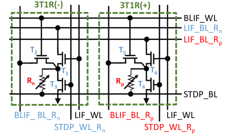
Recently, we proposed a novel PCM-based synapse comprising of two 3T1R (3 transistors, 1 resistor) circuits [39] (See Fig. 1). The two non-volatile PCM-based variable resistors, and , are used to store the signed weight of the synapse. To access the stored weight, two currents are passed through the and in 3T1R(+) and 3T1R(-) circuits, respectively. The difference between the resistance values of and determines the magnitude and sign of the weight. In addition, when placed in a neural circuit with pre and postsynaptic spiking neurons, the two 3T1R circuits can enable asynchronous operation of three fundamental mechanisms in SNNs: a) spike propagation from pre to the postsynaptic neuron, b) spike propagation from post to the presynaptic neuron, and c) weight update based on STDP.
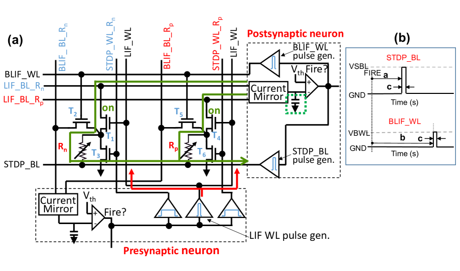
As mentioned in Section I, the capacitor-based LIF neurons [39] are used as pre/postsynaptic neurons in this work. As shown in Fig. 2, the neuron circuits consist of capacitors, current mirrors, comparators, and single-shot pulse generators. The voltage stored in the capacitor () is treated as a membrane potential of the neuron. Using , the current mirror circuits charge and discharge the current based on the resistance values of and . Consequently, will be updated. The current mirror circuit configuration can be found in [39]. If exceeds the pre-defined threshold voltage, , the comparator will generate a spike using the subsequent single-shot pulse generator. Additionally, several other circuits are needed and used in this work to implement the refractory, leaky, and reset behaviors of conventional LIF neurons. The additional circuitry is omitted from the Figs. 2-4 for simplicity. The complete circuit configuration can be found in [39].
Now, let us discuss the three operations of the synapse. First, if the presynaptic neuron fires, a spike will be propagated into the word line, . The red-colored line in Fig. 2 (a) highlights the direction of spike propagation. Consequently, the transistors, , and will be ON and, the current flows from current mirror circuit through and as positive and negative current, respectively. The current directions are highlighted using the green-colored lines in Fig. 2 (a) and the amount of current is determined by Ohm’s law. Then, the current mirror circuit which is connecting to and senses the difference of the positive and the negative current by charging and discharging one capacitor in the postsynaptic neuron. By using this differential sensing scheme, is increased or decreased depending on the polarity and value of the synaptic weight with every incoming spike.
As discussed earlier, if exceeds , the postsynaptic neuron will fire spikes into lines, and . The pulse timing of spikes emitted by the postsynaptic neuron is depicted in Fig. 2 (b). First, a spike will be fired into the bit-line, and this will be used for modifying the resistance values of and . After some delay, the second spike will be fired into the word-line, . Spikes in will be used for transmitting the spiking information from post to the presynaptic neuron.
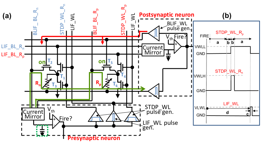
If a postsynaptic neuron fires, a spike will be propagated into (as discussed in the last paragraph). The direction of spike propagation is highlighted by the red-colored line in Fig. 3 (a). Consequently, the transistors, and will be turned ON. Then, the current flows from the current mirror circuit in presynaptic neurons into through and as positive and negative current, respectively. Specifically, positive current flows from to to to and negative current flows from to to to . The current directions are highlighted using the green-colored lines (See Fig. 3 (a)). The of the presynaptic neuron will be either increased or decreased depending on the resistance values of and . If exceeds the , the presynaptic neuron fires spikes into lines, , and . The timing of spikes emitted by the presynaptic neuron is depicted in Fig. 3 (b). First, the spikes will be fired into and . These spikes will be used for modifying the weight based on the STDP rule. Next, a spike will be fired into , and that can be used for transmitting the spiking information from pre to the postsynaptic neuron.
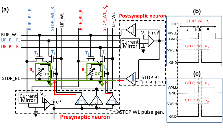
On the other hand, the spikes propagating through the bit-line, , and word-lines, , and enable modification of the weight. For instance, spikes propagating through and will turn ON the transistors, and . The directions of spikes propagating in the circuit are highlighted by the red-colored lines (See Fig. 4 (a)). Concurrently, if a spike propagates through , new current paths will emerge: a) to to to GND and b) to to to GND (as highlighted by the green-colored lines in Fig. 4 (a)). Depending on the magnitude and duration of currents passing through these paths, the resistances of and will be modified. For example, when a spike propagating through has low magnitude and large pulse width as shown in Fig. 4 (b), the resistance value of decreases. In other words, the PCM is being set to the crystalline phase (i.e. low resistance state). However, if a spike propagating in has high magnitude as shown in Fig. 4 (c), the resistance value of will increase. In other words, the PCM cell is changed to an amorphous phase (i.e. high resistance state). If spikes propagating through and as designed with timing diagrams as shown in Fig. 4 (b), will increase and will decrease and the overall weight will be increased. If spikes propagating through and as designed with timing diagrams as shown in Fig. 4 (c), will decrease and will increase and the overall weight will be decreased.
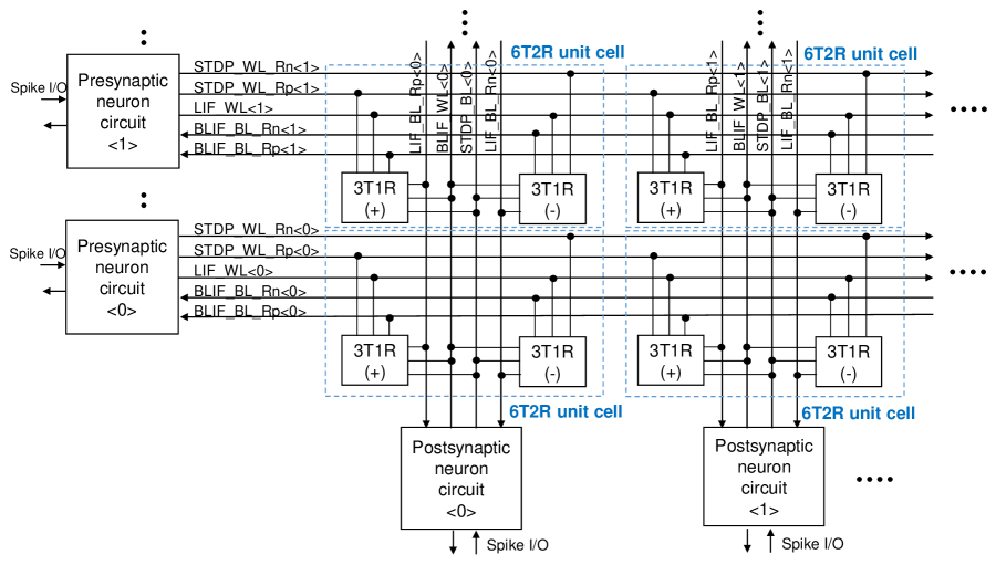
Furthermore, Fig. 5 shows the architecture of Raven designed using the above-discussed synaptic and neural circuits. As shown in Fig. 5, the synaptic circuits are arranged in a crossbar array-like structure with presynaptic neurons in the left and postsynaptic neurons at the bottom. Moreover, the area of an 832832 array connected to 832 presynaptic neurons in the left and 832 postsynaptic neurons at the bottom is estimated to be 2.20 mm2.55 mm [39].
III Speech Command Recognition using Spiking RBMs
The Raven circuits and architectures introduced in Section II can be used to demonstrate the on-chip training and inference of speech commands. We will now discuss the design strategies, algorithms, and neural networks used for such a demonstration.
First, Google’s speech commands dataset is considered [40] in this work. This dataset contains more than 0.1 million utterances of 30 different words. Importantly, it contains words that can be used as commands in the IoT/robotics applications, e.g. stop, go, left, right, up, down, on, off, yes, no, etc. Besides, it also contains the recordings of spoken digits from 0 to 9, various kinds of background noise, and few random utterances (e.g. “happy”, “bird”, “horse”, “tree”, “wow”, etc). Each audio file in the dataset is one-second-long and is sampled at 16 kHz. Throughout this work, 500 audio files of each command are used to create the training datasets and 250 different audio files of each command are used for creating the test datasets.
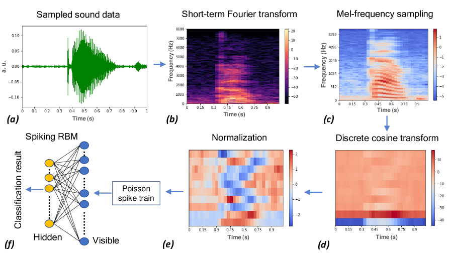
Currently, in most of the automatic speech recognition systems, the sound data is first converted into MFCC images [41], and the images are fed as inputs to the neural networks. Specifically, four main steps listed below are involved in generating the MFCC images.
-
1.
Generate a spectrogram (Fig. 6 (b)) for the sound data of an audio file (Fig. 6 (a)) using Short-Time-Fourier Transforms (STFT). The time-varying sound waves are divided into several small overlapping time frames. The frequencies of sound waves in each time frame are then calculated using the fast Fourier transforms. Note that depending on the size of the time frame and the extent of overlap between the two adjacent frames, the spectrogram can either have better time resolution or frequency resolution.
-
2.
Perform the Mel-frequency sampling on the output spectrogram (Fig. 6 (b)). This sampling re-scales the frequency axis of the spectrogram and emphasizes more on the frequency information in the human’s hearing range.
-
3.
Compress the Mel-sampling output (Fig. 6 (b)) using discrete cosine transforms. This step removes redundant information in the Mel-sampling output.
-
4.
Finally, normalize the compressed output (Fig. 6 (c)). This step reduces the influence of background noise and cancels out the differences in feature maps between different speakers.
As shown in Fig. 6 (e), the final output of these steps is fed as input to the spiking RBMs [57]. RBMs are bi-layer stochastic neural networks with neurons in one layer connected to all the neurons in the other layer, but not connected to neurons within the layer. As shown in Fig. 7, neurons in the first (i.e. visible) layer are divided into three categories-image, label, and bias neurons. The size of input images determines the number of image neurons required in this layer. Similarly, the total number of labels under classification determines the number of label neurons needed. On the other hand, neurons in the second (i.e. hidden) layer are divided into two categories-hidden neurons and bias neurons (See Fig. 7). The hidden neurons learn the features of input images and the number of hidden neurons required depends on the total number of weights required to achieve higher accuracies. Finally, the number of bias neurons required (i.e. in both the visible and hidden layers) needs to be tuned to achieve higher accuracies.
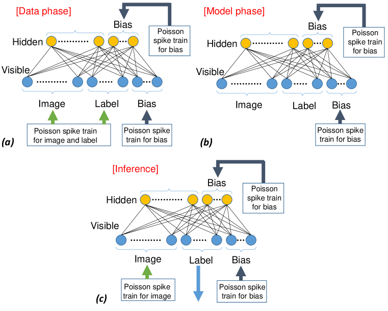
The spiking RBMs are trained with the STDP-based event-driven CD algorithm [42]. Specifically, training is performed in two phases-data phase (Fig. 7 (a)) and model phase (Fig. 7 (b)). In the data phase, images and their labels will be given as inputs to the visible neurons in the form of Poisson spike trains. High (low) pixel values in image results in high (low) spiking rates of corresponding image neurons. Further, if an image belongs to a particular class, only the label neurons related to that class will have high spiking rates and all the others will have low spiking rates. All the bias neurons in visible and hidden layers receive Poisson spike trains with high spiking rates. In the data phase, these externally generated spike trains will propagate from visible to the hidden layer and the weights will be updated positively. Next, in the model phase, no external input spikes are provided to the visible/hidden layer neurons except for the bias neurons. Only the internal spikes and the bias neuron spikes will propagate between the two layers and the weights will be updated negatively. When learning converges, there won’t be any further change in the weight be it in the data phase or model phase.
On the other hand, to perform the inference (Fig. 7 (c)), Poisson spike trains of input images will be provided to the visible neurons. The spikes fired by all the label neurons during the inference period will be counted. The label neurons firing more number of spikes compared to others would be considered as the classification output. For example, when an MFCC image of speech command-“stop” is given as input and the “stop” label neurons fired more spikes than others, the classification output will be “stop”. In contrast, if the “go” label neurons fire more spikes than others, the classification output will be “go”.
Note that all the operations required to be performed in spiking RBMs can be accelerated using the Raven (Fig. 5) introduced in Section. III. The presynaptic neurons connected to the left-side of the synaptic array can be used as visible neurons, whereas the postsynaptic neurons connected at the bottom of the synaptic array can be used as hidden neurons. The input (output) spike trains can be provided (read) using the external spike input (output) circuitry. During the data phase of training, the pulse timings of and can be configured as shown in Fig. 4 (b). In such configuration, will decrease, and will increase and the weight will be updated positively. Similarly, during the model phase of training, the pulse timings of and can be configured as shown in Fig. 4 (c). In such a configuration, will increase, and will decrease and the weight will be updated negatively. Finally, during the inference, the lines, , , and can be disabled and no spikes will propagate through them. Input spike trains of images will be provided to the visible neurons and concurrently, the spikes fired by all the label neurons will be counted using external counters.
IV PCM Hardware-aware Spiking RBM Simulator
We will now discuss the PCM hardware-aware spiking RBM simulator developed to demonstrate the speech command recognition in this work.
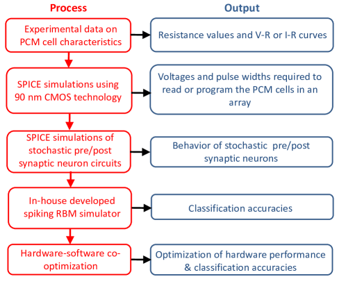
Based on the earlier works on event-driven CD in spiking neuromorphic systems [42], we first developed a spiking RBM simulator that can take sound data as input and perform training and inference operations on the data. This simulator needs several input parameters such as spiking rate, magnitude and pulse width of spikes, equilibrium/rest potential, alpha parameter to update the potential, threshold potential, refractory time, and leak time constant. To estimate these parameters and to take the hardware characteristics/limitations into account, we followed the step-by-step procedure shown in Fig. 8. First, the characteristics of PCM cells such as minimum and maximum resistance values, and current/voltage versus resistance curves are extracted from the experimental data. Next, depending on the size of the synaptic array, the voltages and pulse widths required to read and program the synaptic weights are estimated using SPICE circuit simulations. The behavior of pre and post-synaptic neuron circuits is then studied using SPICE simulations and the abovementioned parameters are estimated and provided as inputs to the spiking RBM simulator, which provides the classification accuracies. Finally, the hardware-software co-optimization is performed based on the classification accuracies and the performance evaluation of circuits in SPICE.
| Quantity | Value |
|---|---|
| Visible neurons | 384 |
| Label neurons in visible layer | 20 |
| Bias neurons in visible layer | 8 |
| Hidden neurons in hidden layer | 500 |
| Bias neurons in hidden layer | 8 |
| Reset/equilibrium potential value | 0 |
| Alpha parameter for updating the potential | 0.06 |
| Threshold potential value | 1 |
| Leak time constant | 1 ms |
| Refractory time period | 4 ms |
| Spiking rate | 20 Hz |
| Quantity | Value |
|---|---|
| VSBL | 2.5 V |
| VBWL, VLWL | 1.2 V |
| VWLL | 0.75 V |
| VWLH | 1.4 V |
| a | 9.1 s (min) - 2040 s (max) |
| b | 4.4 s (min) - 85.8 s (max) |
| c | 20 ns (min) - 79 ns (max) |
| d | 27 s (min) - 4251.6 s (max) |
V Results and Discussion
Using the simulator introduced in Section IV, we will now study the feasibility of performing on-chip training and inference using Raven.
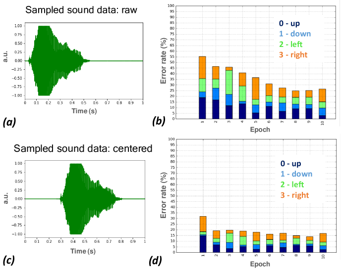
First, the audio files are converted into MFCC images by choosing the size of each time frame in STFT as 160 ms and the overlap between two adjacent frames as 120 ms. Also, 22 frequency bins are used in DCTs. As a result, the output MFCC images have a size of 2222 pixels. Next, these MFCC images are provided as inputs to the spiking RBMs simulator with network parameters tabulated in Table I and the magnitude and pulse widths of spikes used are tabulated in Table II. When a set of four speech commands-up, down, left, and right is considered for training and inference, the best test error rate is found to be 25%. Fig. 9 (b) shows the test error rates observed in each epoch.
The high error rates (See Fig. 9 (b)) arise due to the differences in the exact time at which the commands are uttered in a second. For example, in the sample sound data shown in Fig. 9 (a), the utterance occurred in the first half of a second. If such sound data is used to create an MFCC image, the extracted features will be on the left side of the image (not shown here). Similarly, if the sound data is present in the second half of a second, the extracted features will be on the right side of the image. We found that such variations in the position of features lead to high classification error rates. To resolve this problem, we modified the timing data of each audio file in such a way that the utterance always occur around 0.5 s (as shown in Fig. 9 (c)). As a result, the best test error rate got reduced to 15% as shown in Fig. 9 (d).
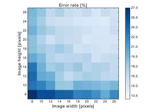
Moreover, as discussed in Section III, the size of input images determine the number of image neurons required and thereby the total number of weights in the network. Furthermore, depending on the image size, the MFCC image can either have better time resolution or frequency resolution, but not both. Therefore, it is crucial to find out the optimum image size required to achieve low classification error rates. The phase diagram is shown in Fig. 10 depicts the dependence of error rates on the input image size. As shown in Fig. 10, low error rates are obtained when the image width/height is between 20 to 24 pixels.
To further reduce the error rates, it is proven in the literature that multiple images of different sizes can be placed side by side and provided as input to the neural networks [58]. We also studied this possibility and found that an error rate of 13.5% can be achieved by using two images of size-1616 and 816. Next, using such a two image configuration, we estimated the classification accuracies for different sets of speech commands and compared them with the results obtained from the state-of-the-art convolution neural networks (CNNs) [43, 44, 45]. As shown in Table III, the minimum (maximum) accuracy difference between CNNs and our work is found to be 5.12% (18.93%). Such an accuracy difference is expected as SNNs with STDP-based learning generally have moderate classification performance when compared to DNNs trained with backpropagation. Currently, there are several on-going research efforts to close the accuracy gap between DNNs and SNNs [59, 60, 61].
| Speech commands | CNNs | our work |
| up, down, left, right | 94.5% | 86.4% |
| bed, cat, happy, bird, five | 91.36% | 86.24% |
| spoken digits [0-9] | 90% | 78.36% |
| stop, go, left, right, on, | ||
| off, up, down, yes, no, | 88.2% | 69.27% |
| silence, unknown |
| Description | WHIFs | WHOFs |
|---|---|---|
| Conv1 | 24161 | 221464 |
| Maxpool1 | 221464 | 11764 |
| Conv2 | 11764 | 9552 |
| Maxpool2 | 9552 | 4252 |
| Conv3 | 4252 | 3136 |
| Maxpool3 | 3136 | 1136 |
| Conv4 | 1136 | 1110 |
| Dense | 1110 | 10 |
Next, to compare the memory and computational requirements of our work with the CNNs at iso-accuracies, we implemented a fully-convolutional neural network (FCNN) [62] with 8 layers as shown in Table IV. In Table IV, and represent the width and height of the feature maps, represent the number of input feature maps provided to each layer, represent the number of output feature maps extracted from each layer. We optimized and the parameters tabulated in Table IV to achieve the same classification accuracies as our work. The backpropagation algorithm with stochastic gradient descent is used to train the FCNNs [8], while the spiking RBMs are trained using event-driven CD algorithm. Note that unlike the spiking RBMs, weights in FCNNs are trained using 32-bit floating-point numbers. The number of parameters, spikes/multiply-and-accumulate operations (MACs), and epochs required to obtain iso-accuracies are estimated and tabulated in Table V. MACs are the fundamental operations required by the CNNs. As shown in Table V, the number of MACs performed in the FCNNs during training and inference is 269.23 and 70.36 greater than the number of spikes generated in the spiking RBMs, respectively. Due to such low computational requirements, the spiking RBM implementation can be more suitable for edge applications, in which accuracies may not be of paramount importance.
| Quantity | Our work | FCNNs |
| Training method | Event-driven CD | Backpropagation |
| with SGD | ||
| Total number of training images | 5000 | 5000 |
| Size of input image | 2416 | 2416 |
| Parameters | 209296 | 38476 |
| Epoch | 6 (batch size = 1) | 3 (batch size = 1) |
| Test accuracy | 78.36% | 78.96% |
| Spikes/MACs during inference | 0.022 M | 1.548 M |
| Spikes/MACs during training | 172.51 M | 46.445 B |
Finally, using the SPICE simulations, we estimated the power and latencies consumed by the Raven circuits and architectures during the training and inference operations. The power and latencies consumed during the training of 5000 MFCC images are estimated to be 30 W (7 W of active power and 23 W of static power) and 3000 sec, respectively. Also, the power and latency consumed for an inference operation on Raven are estimated to be 28 W (5 W of active power and 23 W of static power) and 0.45 sec, respectively. Note that we used the 90 nm CMOS technology for this work.
VI Conclusion
In summary, the ultra-low-power on-chip training and inference of speech commands are demonstrated using the phase change memory (PCM)-based synaptic arrays. The power and latencies consumed during on-chip training (inference) are estimated to be 30 W and 3000 sec (28 W and 0.45 sec). Furthermore, at iso-accuracies, the number of multiply-and-accumulate operations (MACs) needed during the training of a deep neural network (DNN) model is found to be 269.23 greater than the number of spikes required in our work. Similarly, during inference, the number of MACs needed during the inference of DNN is 70.36 greater than the number of spikes required in our work. Overall, due to such low power and computational requirements, the PCM-based synaptic arrays can be promising candidates for enabling AI at the edge.
Acknowledgment
The authors would like to express special thanks to Seiji Munetoh, Atsuya Okazaki, and Akiyo Nomura for their valuable and insightful comments.
References
- [1] S. Deng, H. Zhao, W. Fang, J. Yin, S. Dustdar, and A. Y. Zoa, “Edge intelligence: The confluence of edge computing and artificial intelligence,” IEEE Internet of Things Journal, pp. 1–1, 2020.
- [2] Y. Zhang, X. Ma, J. Zhang, M. S. Hossain, G. Muhammad, and S. U. Amin, “Edge intelligence in the cognitive internet of things: Improving sensitivity and interactivity,” IEEE Network, vol. 33, no. 3, pp. 58–64, 2019.
- [3] Y. Lee, P. Tsung, and M. Wu, “Techology trend of edge ai,” in 2018 International Symposium on VLSI Design, Automation and Test (VLSI-DAT), 2018, pp. 1–2.
- [4] Y. Dai, D. Xu, S. Maharjan, G. Qiao, and Y. Zhang, “Artificial intelligence empowered edge computing and caching for internet of vehicles,” IEEE Wireless Communications, vol. 26, no. 3, pp. 12–18, 2019.
- [5] R. Geirhos, D. H. J. Janssen, H. H. Schütt, J. Rauber, M. Bethge, and F. A. Wichmann, “Comparing deep neural networks against humans: object recognition when the signal gets weaker,” arXiv 1706.06969, 2017.
- [6] C. Seifert, A. Aamir, A. Balagopalan, D. Jain, A. Sharma, S. Grottel, and S. Gumhold, Visualizations of Deep Neural Networks in Computer Vision: A Survey. Springer International Publishing, 2017, pp. 123–144.
- [7] X. Feng, Y. Jiang, X. Yang, M. Du, and X. Li, “Computer vision algorithms and hardware implementations: A survey,” Integration, vol. 69, pp. 309 – 320, 2019.
- [8] D. Rumelhart, G. Hinton, and R. Williams, “Learning representations by back-propagating errors,” Nature, vol. 323, p. 533–536, 1986.
- [9] M. Bali and S. Khurana, “Effect of latency on network and end user domains in cloud computing,” 12 2013, pp. 777–782.
- [10] S. Hu, W. Bai, K. Chen, C. Tian, Y. Zhang, and H. Wu, “Providing bandwidth guarantees, work conservation and low latency simultaneously in the cloud,” IEEE Transactions on Cloud Computing, pp. 1–1, 2018.
- [11] M. Koo, G. Srinivasan, Y. Shim, and K. Roy, “sbsnn: Stochastic-bits enabled binary spiking neural network with on-chip learning for energy efficient neuromorphic computing at the edge,” IEEE Transactions on Circuits and Systems I: Regular Papers, vol. 67, no. 8, pp. 2546–2555, 2020.
- [12] P. Reiter, G. R. Jose, S. Bizmpikis, and I. Cirjila, “Neuromorphic processing and sensing: Evolutionary progression of ai to spiking,” arXiv 2007.05606, 2020.
- [13] M. A. Khoei, A. Yousefzadeh, A. Pourtaherian, O. Moreira, and J. Tapson, “Sparnet: Sparse asynchronous neural network execution for energy efficient inference,” in 2020 2nd IEEE International Conference on Artificial Intelligence Circuits and Systems (AICAS), 2020, pp. 256–260.
- [14] J. M. Allred, S. J. Spencer, G. Srinivasan, and K. Roy, “Explicitly trained spiking sparsity in spiking neural networks with backpropagation,” arXiv 2003.01250, 2020.
- [15] P. Blouw and C. Eliasmith, “Event-driven signal processing with neuromorphic computing systems,” in ICASSP 2020 - 2020 IEEE International Conference on Acoustics, Speech and Signal Processing (ICASSP), 2020, pp. 8534–8538.
- [16] A. Patino-Saucedo, H. Rostro-Gonzaleza, T. Serrano-Gotarredona, and B. Linares-Barrancob, “Event-driven implementation of deep spiking convolutional neural networks for supervised classification using the spinnaker neuromorphic platform,” Neural Networks, vol. 121, pp. 319 – 328, 2020.
- [17] N. Caporale and Y. Dan, “Spike timing–dependent plasticity: A hebbian learning rule,” Annual Review of Neuroscience, vol. 31, no. 1, pp. 25–46, 2008.
- [18] S. Cass, “Taking ai to the edge: Google’s tpu now comes in a maker-friendly package,” IEEE Spectrum, vol. 56, no. 5, pp. 16–17, 2019.
- [19] X. Xu, J. Amaro, S. Caulfield, G. Falcao, and D. Moloney, “Classify 3d voxel based point-cloud using convolutional neural network on a neural compute stick,” in 2017 13th International Conference on Natural Computation, Fuzzy Systems and Knowledge Discovery (ICNC-FSKD), 2017, pp. 37–43.
- [20] S. Cass, “Nvidia makes it easy to embed ai: The jetson nano packs a lot of machine-learning power into diy projects - [hands on],” IEEE Spectrum, vol. 57, no. 7, pp. 14–16, 2020.
- [21] J. Feldmann, K. Kraft, L. Steiner, N. Wehn, and M. Jung, “Fast and accurate dram simulation: Can we further accelerate it?” in 2020 Design, Automation Test in Europe Conference Exhibition (DATE), 2020, pp. 364–369.
- [22] N. Verma, H. Jia, H. Valavi, Y. Tang, M. Ozatay, L. Chen, B. Zhang, and P. Deaville, “In-memory computing: Advances and prospects,” IEEE Solid-State Circuits Magazine, vol. 11, no. 3, pp. 43–55, 2019.
- [23] Z. Zhang, J. Chen, X. Si, Y. Tu, J. Su, W. Huang, J. Wang, W. Wei, Y. Chiu, J. Hong, S. Sheu, S. Li, R. Liu, C. Hsieh, K. Tang, and M. Chang, “A 55nm 1-to-8 bit configurable 6t sram based computing-in-memory unit-macro for cnn-based ai edge processors,” in 2019 IEEE Asian Solid-State Circuits Conference (A-SSCC), 2019, pp. 217–218.
- [24] X. Si, Y. Tu, W. Huanq, J. Su, P. Lu, J. Wang, T. Liu, S. Wu, R. Liu, Y. Chou, Z. Zhang, S. Sie, W. Wei, Y. Lo, T. Wen, T. Hsu, Y. Chen, W. Shih, C. Lo, R. Liu, C. Hsieh, K. Tang, N. Lien, W. Shih, Y. He, Q. Li, and M. Chang, “15.5 a 28nm 64kb 6t sram computing-in-memory macro with 8b mac operation for ai edge chips,” in 2020 IEEE International Solid- State Circuits Conference - (ISSCC), 2020, pp. 246–248.
- [25] J. Nider, C. Mustard, A. Zoltan, and A. Fedorova, “Processing in storage class memory,” in 12th USENIX Workshop on Hot Topics in Storage and File Systems (HotStorage 20), 2020.
- [26] V. Seshadri, D. Lee, T. Mullins, H. Hassan, A. Boroumand, J. Kim, M. A. Kozuch, O. Mutlu, P. B. Gibbons, and T. C. Mowry, “Ambit: In-memory accelerator for bulk bitwise operations using commodity dram technology,” in 2017 50th Annual IEEE/ACM International Symposium on Microarchitecture (MICRO), 2017, pp. 273–287.
- [27] X. Xin, Y. Zhang, and J. Yang, “Elp2im: Efficient and low power bitwise operation processing in dram,” in 2020 IEEE International Symposium on High Performance Computer Architecture (HPCA), 2020, pp. 303–314.
- [28] W. Chen, C. Dou, K. Li, W. Lin, P. Li, J. Huang, J. Wang, W. Wei, C. Xue, Y. Chiu, Y. King, C. Lin, R. Liu, C. Hsieh, K. Tang, J. J. Yang, M. Ho, and M. Chang, “Cmos-integrated memristive non-volatile computing-in-memory for ai edge processors,” Nature Electronics, vol. 2, pp. 420–428, 2019.
- [29] X. Wang, M. A. Zidan, and W. D. Lu, “A crossbar-based in-memory computing architecture,” IEEE Transactions on Circuits and Systems I: Regular Papers, pp. 1–9, 2020.
- [30] B. Gao, “Emerging non-volatile memories for computation-in-memory,” in 2020 25th Asia and South Pacific Design Automation Conference (ASP-DAC), 2020, pp. 381–384.
- [31] A. Sebastian, M. L. Gallo, R. Khaddam-Aljameh, and E. Eleftheriou, “Memory devices and applications for in-memory computing,” Nature Nanotechnology, vol. 15, pp. 529–544, 2020.
- [32] S. R. Nandakumar, I. Boybat, M. L. Gallo, E. Eleftheriou, A. Sebastian, and B. Rajendran, “Experimental demonstration of supervised learning in spiking neural networks with phase-change memory synapses,” Scientific Reports, vol. 10, no. 8080, 2020.
- [33] S. Ambrogio, P. Narayanan, H. Tsai, R. M. Shelby, I. Boybat, C. D. Nolfo, S. Sidler, M. Giordano, M. Bodini, N. C. P. Farinha, B. Killeen, C. Cheng, Y. Jaoudi, and G. W. Burr, “Equivalent-accuracy accelerated neural-network training using analogue memory,” Nature, vol. 558, pp. 60–67, 2018.
- [34] I. Boybat, M. L. Gallo, S. R. Nandakumar, T. Moraitis, T. Parnell, T. Tuma, B. Rajendran, Y. Leblebici, A. Sebastian, and E. Eleftheriou, “Neuromorphic computing with multi-memristive synapses,” Nature Communications, vol. 9, no. 2514, 2018.
- [35] M. Hu, J. P. Strachan, Z. Li, E. M. Grafals, N. Davila, C. Graves, S. Lam, N. Ge, J. J. Yang, and R. S. Williams, “Dot-product engine for neuromorphic computing: Programming 1t1m crossbar to accelerate matrix-vector multiplication,” in 2016 53nd ACM/EDAC/IEEE Design Automation Conference (DAC), 2016, pp. 1–6.
- [36] H. Lue, P. Hsu, M. Wei, T. Yeh, P. Du, W. Chen, K. Wang, and C. Lu, “Optimal design methods to transform 3d nand flash into a high-density, high-bandwidth and low-power nonvolatile computing in memory (nvcim) accelerator for deep-learning neural networks (dnn),” in 2019 IEEE International Electron Devices Meeting (IEDM), 2019, pp. 38.1.1–38.1.4.
- [37] P. Du, H. Lue, T. Hsu, C. Hsieh, W. Chen, K. Chang, K. Wang, and C. Lu, “Read disturb evaluations of 3d nand flash for highly read-intensive edge-computing inference device for artificial intelligence applications,” in 2019 IEEE 11th International Memory Workshop (IMW), 2019, pp. 1–4.
- [38] Y. Xiang, P. Huang, R. Han, C. Li, K. Wang, X. Liu, and J. Kang, “Efficient and robust spike-driven deep convolutional neural networks based on nor flash computing array,” IEEE Transactions on Electron Devices, vol. 67, no. 6, pp. 2329–2335, 2020.
- [39] M. Ishii, S. Kim, S. Lewis, A. Okazaki, J. Okazawa, M. Ito, M. Rasch, W. Kim, A. Nomura, U. Shin, K. Hosokawa, M. BrightSky, and W. Haensch, “On-chip trainable 1.4m 6t2r pcm synaptic array with 1.6k stochastic lif neurons for spiking rbm,” in 2019 IEEE International Electron Devices Meeting (IEDM), 2019, pp. 14.2.1–14.2.4.
- [40] Google, https://ai.googleblog.com/2017/08/launching-speech-commands-dataset.html, 2017.
- [41] H. Mukherjee, A. Dhar, S. M. Obaidullah, S. Phadikar, and K. Roy, “Image-based features for speech signal classification,” Multimedia Tools and Applications, 2020.
- [42] N. Emre, S. Das, B. Pedroni, K. D. Kenneth, and G. Cauwenberghs, “Event-driven contrastive divergence for spiking neuromorphic systems,” Frontiers in Neuroscience, vol. 7, p. 272, 2014.
- [43] P. Warden, “Speech commands: A dataset for limited-vocabulary speech recognition,” arXiv 1804.03209, 2018.
- [44] X. Li and Z. Zhou, “Speech command recognition with convolutional neural network,” Stanford CS 229 projects, 2019. [Online]. Available: http://cs229.stanford.edu/proj2017/final-reports/5244201.pdf
- [45] A. C. Patil and H. Lee, “Speech to text translation using google speech commands,” Stanford CS 229 projects, 2019. [Online]. Available: http://cs229.stanford.edu/proj2019aut/data/assignment_308832_raw/26647342.pdf
- [46] G. W. Burr, M. J. Breitwisch, M. Franceschini, D. Garetto, K. Gopalakrishnan, B. Jackson, B. Kurdi, C. Lam, L. A. Lastras, A. Padilla, B. Rajendran, S. Raoux, and R. S. Shenoy, “Phase change memory technology,” Journal of Vacuum Science & Technology B, vol. 28, no. 2, pp. 223–262, 2010.
- [47] B. R. Anupama, U. C. Sahooa, and P. Rathb, “Phase change materials for pavement applications: A review,” Construction and Building Materials, vol. 247, p. 118553, 2020.
- [48] H. P. Wong, S. Raoux, S. Kim, J. Liang, J. P. Reifenberg, B. Rajendran, M. Asheghi, and K. E. Goodson, “Phase change memory,” Proceedings of the IEEE, vol. 98, no. 12, pp. 2201–2227, 2010.
- [49] W. Kim, R. L. Bruce, T. Masuda, G. W. Fraczak, N. Gong, P. Adusumilli, S. Ambrogio, H. Tsai, J. Bruley, J. . Han, M. Longstreet, F. Carta, K. Suu, and M. BrightSky, “Confined pcm-based analog synaptic devices offering low resistance-drift and 1000 programmable states for deep learning,” in 2019 Symposium on VLSI Technology, 2019, pp. T66–T67.
- [50] T. Kim and S. Lee, “Evolution of phase-change memory for the storage-class memory and beyond,” IEEE Transactions on Electron Devices, vol. 67, no. 4, pp. 1394–1406, 2020.
- [51] F. Arnaud, P. Zuliani, J. P. Reynard, A. Gandolfo, F. Disegni, P. Mattavelli, E. Gomiero, G. Samanni, C. Jahan, R. Berthelon, O. Weber, E. Richard, V. Barral, A. Villaret, S. Kohler, J. C. Grenier, R. Ranica, C. Gallon, A. Souhaite, D. Ristoiu, L. Favennec, V. Caubet, S. Delmedico, N. Cherault, R. Beneyton, S. Chouteau, P. O. Sassoulas, A. Vernhet, Y. L. Friec, F. Domengie, L. Scotti, D. Pacelli, J. L. Ogier, F. Boucard, S. Lagrasta, D. Benoit, L. Clement, P. Boivin, P. Ferreira, R. Annunziata, and P. Cappelletti, “Truly innovative 28nm fdsoi technology for automotive micro-controller applications embedding 16mb phase change memory,” in 2018 IEEE International Electron Devices Meeting (IEDM), 2018, pp. 18.4.1–18.4.4.
- [52] EETimes, https://www.eetimes.com/phase-change-memory-found-in-handset/, 2010.
- [53] M. L. Gallo, A. Sebastian, R. Mathis, M. Manica, H. Giefers, T. Tuma, C. Bekas, A. Curioni, and E. Eleftheriou, “Mixed-precision in-memory computing,” Nature Electronics, vol. 1, pp. 246–253, 2018.
- [54] L. Wang, W. Gao, L. Yu, J. Wu, and B. Xiong, “Multiple-matrix vector multiplication with crossbar phase-change memory,” Applied Physics Express, vol. 12, no. 10, p. 105002, 2019.
- [55] C. D. Wright, Y. Liu, K. I. Kohary, M. M. Aziz, and R. J. Hicken, “Arithmetic and biologically-inspired computing using phase-change materials,” Advanced Materials, vol. 23, no. 30, pp. 3408–3413, 2011.
- [56] G. W. Burr, R. M. Shelby, A. Sebastian, S. Kim, S. Kim, S. Sidler, K. Virwani, M. Ishii, P. Narayanan, A. Fumarola, L. L. Sanches, I. Boybat, M. L. Gallo, K. Moon, J. Woo, H. Hwang, and Y. Leblebici, “Neuromorphic computing using non-volatile memory,” Advances in Physics: X, vol. 2, no. 1, pp. 89–124, 2017.
- [57] P. Smolensky, “Information processing in dynamical systems: Foundations of harmony theory ; cu-cs-321-86,” Computer Science Technical Reports, vol. 315, 1986.
- [58] T. T. Doroteo, M. P. Fernández-Gallego, and A. Lozano-Diez, “Multi-resolution speech analysis for automatic speech recognition using deep neural networks: Experiments on timit,” PLOS ONE, vol. 13, no. 10, pp. 1–24, 2018.
- [59] J. Kim, C. Kim, S. Y. Woo, W. Kang, Y. Seo, S. Lee, S. Oh, J. Bae, B. Park, and J. Lee, “Initial synaptic weight distribution for fast learning speed and high recognition rate in stdp-based spiking neural network,” Solid-State Electronics, vol. 165, p. 107742, 2020.
- [60] L. Deng, Y. Wu, X. Hu, L. Liang, Y. Ding, G. Li, G. Zhao, P. Li, and Y. Xie, “Rethinking the performance comparison between snns and anns,” Neural Networks, vol. 121, pp. 294 – 307, 2020.
- [61] P. Falez, P. Tirilly, and I. M. Bilasco, “Improving stdp-based visual feature learning with whitening,” arXiv 2002.10177, 2020.
- [62] J. Long, E. Shelhamer, and T. Darrell, “Fully convolutional networks for semantic segmentation,” in 2015 IEEE Conference on Computer Vision and Pattern Recognition (CVPR), 2015, pp. 3431–3440.