Lattice dynamics of endotaxial silicide nanowires
Zusammenfassung
Self-organized silicide nanowires are considered as main building blocks of future nanoelectronics and have been intensively investigated. In nanostructures, the lattice vibrational waves (phonons) deviate drastically from those in bulk crystals, which gives rise to anomalies in thermodynamic, elastic, electronic, and magnetic properties. Hence, a thorough understanding of the physical properties of these materials requires a comprehensive investigation of the lattice dynamics as a function of the nanowire size. We performed a systematic lattice dynamics study of endotaxial FeSi2 nanowires, forming the metastable, surface-stabilized -phase, which are in-plane embedded into the Si(110) surface. The average widths of the nanowires ranged from 24 to 3 nm, their lengths ranged from several m to about 100 nm. The Fe-partial phonon density of states, obtained by nuclear inelastic scattering, exhibits a broadening of the spectral features with decreasing nanowire width. The experimental data obtained along and across the nanowires unveiled a pronounced vibrational anisotropy that originates from the specific orientation of the tetragonal -FeSi2 unit cell on the Si(110) surface. The results from first-principles calculations are fully consistent with the experimental data and allow for a comprehensive understanding of the lattice dynamics of endotaxial silicide nanowires.
I Introduction
Metallic silicides constitute an important part of current microelectronics, serving as Schottky barriers and ohmic contacts, gate electrodes, local interconnects and diffusion barriers Murarka (1995); Chen_book (2004); Chen (2005). The enormous degree of miniaturization of nowadays integrated circuits imposes severe restrictions on the spatial dimensions of these components. New materials and configurations are constantly researched for nanoelectronic applications and endotaxial silicide nanowires (NWs), self-organized on the Si surface, have been considered as promising candidates Bennett et al. (2011). The endotaxial mechanism implies the formation of in-plane unidirectionally aligned, high-aspect ratio NWs grown partially into the substrate He et al. (2004). These nanostructures are readily integrated with Si technology and exhibit high crystal-phase purity and thermal stability, sharp interfaces and Schottky barrier heights which are tunable by the choice of silicide material Mahato et al. (2017). FeSi2 is a particularly attractive silicide since it exhibits several crystal phases, namely the room-temperature stable semiconducting -phase, high-temperature metallic -phase and surface-stabilized metallic - and -phases Bennett et al. (2011). Due to the very small lattice mismatch with certain crystallographic planes of Si, the tetragonal -FeSi2 can also be stabilized at room temperature in epitaxial nanostructures on Si surfaces. However, the reports about the crystal structure of FeSi2 NWs formed on Si(110) remain contradictory, spanning cubic ( or ) Liang et al. (2006, 2006); Das et al. (2014) and tetragonal () Zou et al. (2017) phases.
When the dimensions of nanostructures approach the characteristic phonon mean free paths (from several nanometers up to micrometers), the phonon dispersions and the phonon density of states (PDOS), which characterize the lattice dynamics of a material, begin to deviate from those of the bulk counterparts. These deviations imply significant modifications of thermodynamic and elastic properties, which are directly related to the lattice dynamics, such as lattice heat capacity, vibrational entropy, mean force constants, sound velocity and thermal conductivity. They also lead to an enhanced electron-phonon, spin-phonon and phonon-phonon scattering at surfaces and interfaces Bozyigit et al. (2016). In conjunction with a possible emergence of phonon quantum phenomena at very small dimensions Hepplestone (2005), these effects could significantly deteriorate the electron and spin transport in nanoscale interconnects Steinhögl et al. (2002); Rideau et al. (2011); Tobler et al. (2015).
The phonon dispersions and PDOS of 1D nanostructures have been subjects of intensive theoretical studies, predicting features that differ significantly from those in the 3D counterparts. The most prominent effects are confined bands and band gaps, acoustic modes with non-zero frequencies at ( is the phonon wave vector), non-linear dispersion for small and a complex displacement field Nishiguchi et al., (1997); Mukdadi et al., (1997); Srivastava (2006); Allen (2007); Mizuno et al., (2009); Sengün (2010); Velasco (2011); Mizuno (2014); Saviot (2018). Consequently, anomalies in thermal conductivity Zou (2001); Glavin (2001); Lü (2006); Qiu (2011); Karamitaheri (2014); Zhou (2017); Rashid (2018); Qiu (2011) and electron-phonon interactions Nishiguchi (2002); Uno (2011); Yamada (2012); Tienda-Luna (2013) were predicted and strategies for their tailoring in NWs were suggested Malhotra (2019).
Unlike the intensive theoretical studies, the experimental reports on lattice dynamics of NWs remain scarce. Optical phonon confinement phenomena in Si Li et al. (1999); Wang et al. (2000); Piscanec et al. (2003); Adu et al. (2005); Patsha et al. (2018) and III-V Luca et al. (2019) NWs were studied by Raman spectroscopy. Resonant and propagative coherent acoustic phonon modes were investigated by time-resolved spectroscopy with visible light Mante et al. (2018) and x-rays Mariager et al. (2010). Using Brillouin-Mandelstam light scattering spectroscopy, surprisingly strong confinement effects in the acoustic phonon dispersions were observed in individual GaAs NWs with diameters exceeding by an order of magnitude the phonon mean-free path Kargar et al. (2016). Employing nuclear inelastic scattering (NIS) on the 125Te isotope, the Te-partial PDOS of Bi2Te3 NWs array with an average NW diameter of 56 nm was determined, unveiling a reduction of the speed of sound by 7 % compared to the bulk material Bessas et al. (2013). By application of the same experimental technique on the 119Sn resonance, a correlation between the lattice softening in Sn NWs with a diameter between 100 and 18 nm and an increase of the critical temperature of the superconducting state was established Temstögl et al. (2019). Despite their potential applications in nanoelectronics, the lattice dynamics of endotaxial silicide NWs remains unexplored.
Here we present a systematic lattice dynamics study of endotaxial FeSi2 NWs formed on Si(110) for a large range of sizes. The Fe-partial PDOS exhibits a broadening of the spectral features with decreasing NW width. The experimental data obtained along and across the NWs unveil a pronounced vibrational anisotropy that originates from the specific orientation of the tetragonal -FeSi2 unit cell on the Si(110) surface and is fully consistent with the results from first-principles calculations.
II Experimental and theoretical details
Endotaxial FeSi2 NWs were grown on the 16 2 reconstructed Si(110) surface under ultra high vacuum (UHV) conditions (P110-8 Pa). The substrates were degassed in UHV at 650C for 4 h, followed by the removal of the native SiO2 layer by heating two times to 1250C for 30 seconds. Subsequently, the Si(110) surface was stabilized at the growth temperature and a certain amount of high purity iron, enriched to 96 % in the Mössbauer-active isotope 57Fe, was deposited. The coverage was controlled by a quartz oscillator with an accuracy of 10 % and is given in monolayer (ML) units, with 1 ML = 4.78 1014 Fe atoms/cm2. Details of the growth and experimental conditions used for the investigated samples, hereinafter referred to as S1-S7, are summarized in Table 1. All measurements described in the following were conducted at room temperature. The crystal structure of the samples was investigated with reflection high-energy electron diffraction (RHEED), the surface topography was determined by non-contact atomic force microscopy (AFM) in an Omicron Large Sample scanning probe microscope connected to the UHV-cluster. Samples S1, S2, S3, S5 and S6 were subsequently capped with 4 nm of amorphous Si sputtered at room temperature in a chamber Krause et al. (2012) with a base pressure of P110-6 Pa also connected to the UHV-cluster. The flux of the sputter gas Ar was 0.8 sccm, corresponding to a pressure of 0.36 Pa.
The local crystal structure of the NWs in S2, S6 and S7 was investigated by Fe -edge x-ray absorption spectroscopy at the SUL-X beamline of the synchrotron radiation source KARA at KIT. After calibration with an -Fe metal foil to the Fe -edge at 7112 eV, the fluorescence emission of the samples was recorded up to Å-1. The incoming x-ray beam was parallel to Si[], i.e. oriented along the NWs. A beam-to-sample-to-detector geometry of 45∘/45∘ was applied, using a collimated x-ray beam of about 0.8 mm 0.8 mm, or focused x-ray beam with 0.35 mm 0.15 mm (h v, FWHM) at the sample position. The obtained extended x-ray absorption fine structure (EXAFS) spectra were processed with the ATHENA and ARTEMIS programs included in the IFEFFIT package Ravel et al. (2005). The spectra were weighted by , , within a -range of 3.8 - 13.2 Å-1. The data was modeled in the real space with Hanning windows and = 2 within a range of 1.0 - 2.7 Å using a shell-by-shell approach. Multiple scattering paths do not contribute in the modeled R region. The single scattering paths were calculated with FEFF6 for the crystal structure of -FeSi2. The amplitude reduction factor was set to 0.7 and was fixed during the fitting process. It was obtained by modeling the EXAFS spectrum of the -Fe foil used for calibration. The Debye-Waller factors of Si were variable fit parameters, whereas for Fe they were fixed to the values obtained from the NIS experiment.
| Sample | [ML] | [C] | [nm] | NIS exp. |
|---|---|---|---|---|
| S1 | 3 0.3 | 825 20 | 24 7 | Si cap |
| S2 | 6 0.6 | 700 10 | 18 5 | Si cap |
| S3 | 2 0.2 | 700 10 | 10 3 | Si cap |
| S4 | 2 0.2 | 700 10 | 11 3 | in situ |
| S5 | 1.5 0.2 | 600 10 | 4 1 | Si cap |
| S6 | 1 0.1 | 600 10 | 3 1 | Si cap |
| S7 | 4 0.3 | 825 20 | 26 7 | - |
The Fe-partial PDOS was obtained Kohn and Chumakov (2000) by NIS experiments Seto_PRL_NIS ; Sturhahn_PRL_NIS performed at the Dynamics Beamline P01 Wille et al. (2010) at PETRA III and the Nuclear Resonance Beamline ID18 Rüffer and Chumakov (1996) at the ESRF. At both beamlines the measurements were performed in grazing-incidence geometry with an incidence angle < 0.2∘ and an x-ray beam with dimensions of 1.5 mm 0.01 mm (h v, FWHM). The energy dependence of the probability for nuclear inelastic absorption was measured by tuning the energy of the x-ray beam around the 57Fe resonance at 14.413 keV with an energy resolution of 0.7 meV for S1, S2 (ID18), 1.0 meV for S3, S4 (P01) and 1.3 meV for S5, S6 (P01). Sample S4 was transported to the beamline and measured under UHV condition (P510-7 Pa) in a dedicated chamber Ibrahimkutty et al. (2015).
First-principles calculations were performed within the density functional theory implemented in the VASP code vasp1 ; vasp2 , employing the generalized gradient approximation PBE1 ; PBE2 . The phonon dispersions and PDOS were calculated using the direct method phonon1 incorporated into the PHONON program phonon2 . To account for the tensile epitaxial strain between the FeSi2 crystal and the Si(110) surface, the calculations were done for 0.5 % tensile-strained -phase FeSi2 ( Å, Å). Further details are given elsewhere Kalt et al. (2020).
To ensure a valid comparison of the parameters obtained by fitting the experimental data with the ab initio calculated PDOS, the energy resolution each sample was measured with was considered. The ab initio calculated energy dependence of the probability for nuclear inelastic absorption was convoluted with a Voigt profile with the FWHM corresponding to the energy resolution used for the respective sample. Subsequently, the PDOS used for the fitting process of each sample was calculated.
III Results and discussion
III.1 Structural investigation
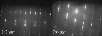
Figure 1 shows generic RHEED patterns of NWs obtained with the wave vector of the electron beam being oriented (a) 90∘ and (b) 35∘ with respect to the NWs. At 90∘ the pattern is composed of several diffraction spots superimposed on straight streaks. When the angle between the NWs and the wave vector of the electron beam is reduced to 35∘, the streaks are bended and the diffraction spots follow their curvature. This observation is explained by the reciprocal space planes of one-dimensional atomic chains with high crystalline order along the chain orientation 1d_RHEED_theo ; dobson1982_GaAs_domain ; 1d_RHEED_exp and confirms the formation of single-crystalline, unidirectionally aligned NWs. The RHEED images obtained for S1-S6 revealed the same pattern throughout the entire range of growth parameters, indicating that for all samples the NWs exhibit the same crystal structure. A detailed discussion of the RHEED results is given in the Supplemental Material sm .
| scattering path | (10-2Å2) | coord. number | d (Å) | |
|---|---|---|---|---|
| S7 | Fe-Si | 0.41 0.05 | 7.4 0.4 | 2.36 0.01 |
| Fe-Fe | 1.00 0.02 | 2.6 0.3 | 2.68 0.01 | |
| S2 | Fe-Si | 0.41 0.04 | 7.3 0.3 | 2.35 0.01 |
| Fe-Fe | 1.01 0.02 | 2.8 0.3 | 2.67 0.01 | |
| S6 | Fe-Si | 0.52 0.08 | 6.6 0.5 | 2.35 0.01 |
| Fe-Fe | 1.05 0.02 | 2.3 0.5 | 2.69 0.01 | |
| -phase | Fe-Si | - | 8 | 2.36 |
| Fe-Fe | - | 2 | 2.70 | |
| -phase | Fe-Si | - | 6 | 2.36 |
| Fe-Fe | - | 2 | 2.97 | |
| s-phase | Fe-Si | - | 4 | 2.39 |
| Fe-Fe | - | 4 | 2.76 | |
| -phase | Fe-Si | - | 4 | 2.33 |
| Fe-Fe | - | 10 | 3.81 |
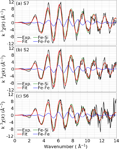
In Fig. 2 the experimental EXAFS spectra in space of samples S7, S2 and S6 are compared to the respective best fit results. Since S7 was grown at very similar conditions as S1 (see Table 1), it is concluded that the NWs of these two samples exhibit the same crystal structure. In Table 2 the interatomic distances and coordination numbers of the Si and Fe nearest neighbors, obtained by modeling of the experimental data, are compared with the values theoretically predicted for the FeSi2 phases formed on Si surfaces. For the determination of the theoretical values it has to be considered that in single crystals the intensity of the EXAFS signal depends on the orientation of the incoming x-ray beam relative to the crystal axes. All spectra were measured with the wave vector of the x-ray beam being parallel to the NWs, i.e. oriented along Si[]. The crystal directions being parallel to Si[] are: -FeSi2[], -FeSi2[], -FeSi2[] and s-FeSi2[]. Correspondingly, the coordination numbers given in Table 2 were calculated with the x-ray beam projected along the respective FeSi2 crystal direction. The results for both parameters exclude the formation of -, - or -FeSi2 and, in agreement with an earlier report Zou et al. (2017), reveal that the investigated NWs exhibit the tetragonal -phase. Furthermore, the values obtained from the modeling of the EXAFS data show an increase of the Debye-Waller factor of the Si atoms in the smallest wires (S6). The fit results for the interatomic distances do not show a size-dependent behavior, while the coordination numbers for Fe-Si and Fe-Fe are reduced in S6 compared to S7 and S2. The reason for this is the increased interface-to-volume ratio in the smallest NWs of S6 compared to S7 and S2.
For the growth of -FeSi2 on Si() Kalt et al. (2020); Berbezier et al. (1994); Kataoka et al. (2006) and Si() chen_alpha_wires ; won_alpha_2006 the commonly reported epitaxial relation is Si{}-FeSi2{}. In this configuration, the lattice mismatch is minimized if Si-FeSi Berbezier et al. (1994). Translated on the Si() surface, this leads to: Si()-FeSi2() and Si[]-FeSi2[]. In Fig. 3 the corresponding orientation of the -FeSi2 unit cell on the Si() surface is depicted. The lattice mismatch (defined as )) is 0.5 % along Si[] and 1 % along Si[] and the tilt angle between -FeSi2[] and Si[] amounts to 18∘. Furthermore, this configuration implies that -FeSi2[] is 0.5∘ off Si[].
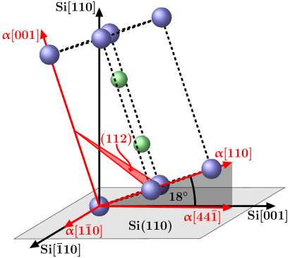
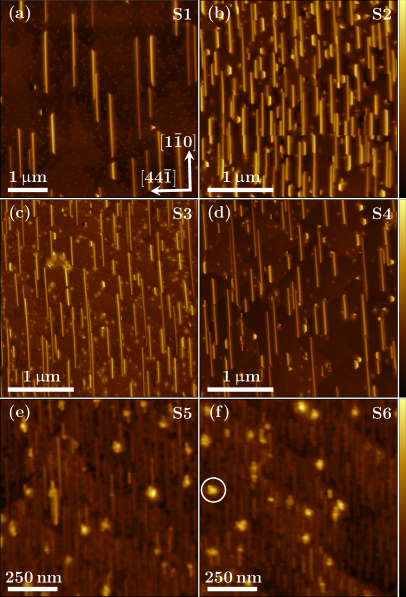
Figure 4 shows an overview of the AFM images of S1-S6. For all samples the NWs are unidirectionally aligned along Si[], as reported for the growth of FeSi2 on Si() He et al. (2004); Zou et al. (2017); Das et al. (2014); Liang et al. (2006). The epitaxial relation discussed above implies that the NWs are formed along Si[]-FeSi2[]. Furthermore, due to the small deviation of 0.5∘ we approximate that Si[]-FeSi2[] (Fig. 4 (a)). The average width of the NWs, calculated from AFM line scans sm , are given in Table 1. As expected, an increase of the growth temperature or the amount of deposited iron leads to NWs with larger dimensions. The AFM images of S5 and S6 exhibit additional round islands, an example is marked in Fig. 4 (f). These structures occur after the removal of the native SiO2 layer and by x-ray photoelectron spectroscopy were identified as a copper contamination. Since the NIS technique is sensitive solely to the 57Fe nuclei Seto_PRL_NIS ; Sturhahn_PRL_NIS ; Chumakov and Sturhahn (1999), the Cu islands do not contribute to the obtained PDOS of the NWs.
III.2 Lattice dynamics
In Fig. 5 the Fe-partial PDOS of S1-S6 obtained with the wave vector of the x-ray beam being parallel to -FeSi2[] (left column) and -FeSi2[] (right column) are depicted. A comparison of the PDOS obtained along and across the NWs shows a vibrational anisotropy with pronounced differences around 20 meV. Furthermore, the reduction of the average NW width from 24 nm (S1) to 3 nm (S6) leads to a broadening of the peaks.
Previous ab initio calculations of the direction-projected Fe-partial PDOS of the tetragonal -FeSi2 showed a decoupling of vibrations with xy- and z-polarization Kalt et al. (2020). The Fe-partial PDOS of the xy-polarized vibrations consists of peaks at 24, 33, and 45 meV, while the z-polarized vibrations are mostly localized at 20 meV with a minor plateau around 40 meV. The experimental PDOS obtained with the wave vector of the x-ray beam being parallel to a certain crystallographic direction of the NWs is composed of a specific combination of xy- and z-polarized phonons Kalt et al. (2020); Chumakov et al. (1997); Kohn et al. (1998). The relative contributions of xy-, () and z- () polarized phonons can be calculated sm considering the orientation of the -FeSi2 unit cell and amount to =1 and =0 for -FeSi2[] and =0.9 and =0.1 for -FeSi2[]. Consequently, the observed vibrational anisotropy originates from the specific orientation of the -FeSi2 unit cell on the Si(110) surface (see Fig. 3).
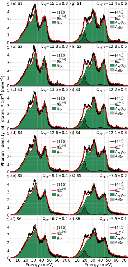
The observed damping of the PDOS features upon reduction of the NW size can be quantified by comparison of the experimental results with the ab initio calculations Kalt et al. (2020). The damping originates from phonon scattering at defects at interfaces and surfaces, as well as within the crystal Fultz (2010) and can be described by the damped harmonic oscillator (DHO) function Faak1 . The DHO function introduces an energy-dependent broadening of the spectral features quantified by the quality factor , which is inversely proportional to the strength of the damping. The experimental PDOS data were modeled by convolution of the ab initio calculated PDOS, obtained for a 0.5 % tensile strained -FeSi2 crystal, with the DHO function. The strength of the damping in the respective sample is quantified by the values obtained using the least-squares method.
For measurements along -FeSi2[] (along the NWs), the PDOS consists of xy-polarized vibrations only and the experimental data can be described by:
| (1) |
with being the ab initio calculated xy-polarized Fe-partial PDOS convoluted with the DHO function with a quality factor . In Fig. 5 (a)-(f) is compared with the respective experimental PDOS. In general, a very good agreement is observed between experiment and theory. While the peak around 45 meV occurs at the same positions in the experimentally determined and ab initio calculated PDOS, the minor peak around 25 meV is shifted by 1.5 meV to lower energy and the peak around 33 meV is shifted by about 1 meV to higher energy in the ab initio calculated PDOS. Most likely these differences occur due to a more complicated strain distribution in the -FeSi2 crystal than the assumed isotropic 0.5 % tensile strain.
The PDOS obtained along -FeSi2[] (across the NWs) is modeled by the weighted sum of the ab initio calculated xy- and z-polarized PDOS, convoluted with the DHO function with a quality factor :
| (2) |
In Fig. 5 (g)-(l) is plotted with the respective xy- () and z- () contributions and the corresponding values obtained from the fit note_Axy_Az . A very good agreement between experiment and theory is observed. The peak of the z-polarized phonons around 20 meV occurs at the same energies in theory and experiment. The xy-polarized vibrations along -FeSi2[] are also well reproduced by the model, except for small shifts of the peaks at 25 and 33 meV, which are also observed in the measurements along -FeSi2[] and are attributed to a complex strain distribution. On average, the values obtained for the PDOS across the NWs are reduced by 10 % compared to the values obtained for the PDOS along the NWs. The reason for the slightly stronger damping of the phonons propagating across the NWs could be the smaller size of the -FeSi2 crystal along this direction.
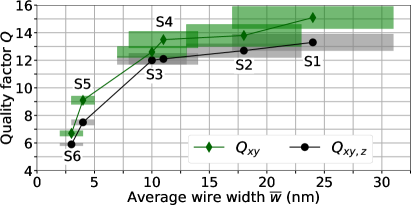
In Fig. 6 the quality factors obtained from the least squares fits for S1-S6 along [] and [] are depicted as a function of . The and values of S1-S4 show a slight decrease in the range of 24 nm 10 nm, whereas upon reduction of below 10 nm in S5 and S6 and are significantly reduced. To comprehend this trend, the interface-to-volume ratio of the NWs has to be considered. In the volume part, i.e. the core of the NWs, the atoms are located in a bulk-like environment with a high degree of crystalline order. At the interface towards the substrate the defect density is generally increased and thus the scattering of phonons is enhanced. For the small wires of S5 and S6 the interface-to-volume ratio is significantly higher and consequently and are distinctly reduced.
| direction | (Å2) | () | () | () | |||
|---|---|---|---|---|---|---|---|
| Theory | [] | 254 5 | 0.0096 0.0002 | 2.62 0.02 | 2.60 0.02 | - | 4988 |
| [] | 245 5 | 0.0096 0.0002 | 2.68 0.02 | 2.61 0.02 | - | - | |
| S1 | [] | 249 5 | 0.0100 0.0002 | 2.69 0.02 | 2.61 0.02 | 3.200.04 | 4700 50 |
| [] | 245 5 | 0.0104 0.0002 | 2.74 0.02 | 2.62 0.02 | 3.030.07 | 4780 100 | |
| S2 | [] | 250 5 | 0.0101 0.0002 | 2.67 0.02 | 2.60 0.02 | 3.510.07 | 4550 100 |
| [] | 245 5 | 0.0105 0.0002 | 2.73 0.02 | 2.61 0.02 | 3.240.08 | 4670 120 | |
| S3 | [] | 248 5 | 0.0101 0.0002 | 2.67 0.02 | 2.60 0.02 | 3.380.06 | 4600 80 |
| [] | 247 5 | 0.0105 0.0002 | 2.72 0.02 | 2.61 0.02 | 3.370.07 | 4610 100 | |
| S4 | [] | 256 5 | 0.0096 0.0002 | 2.64 0.02 | 2.59 0.02 | 3.010.09 | 4780 140 |
| [] | 251 5 | 0.0102 0.0002 | 2.69 0.02 | 2.59 0.02 | 3.130.04 | 4730 60 | |
| S5 | [] | 259 5 | 0.0104 0.0002 | 2.66 0.02 | 2.59 0.02 | 3.690.04 | 4480 50 |
| [] | 250 5 | 0.0110 0.0002 | 2.74 0.02 | 2.60 0.02 | 3.820.05 | 4420 60 | |
| S6 | [] | 255 5 | 0.0105 0.0002 | 2.68 0.02 | 2.59 0.02 | 3.960.05 | 4370 60 |
| [] | 255 5 | 0.0110 0.0002 | 2.71 0.02 | 2.60 0.02 | 4.000.05 | 4360 60 |
A study of the lattice dynamics of epitaxial -FeSi2 nanoislands on Si(111) unveiled a polarization-dependence of the phonon damping, i.e. a stronger damping of z-polarized phonons, in islands with average heights below 10 nm Kalt et al. (2020). To examine if this effect is also present in the investigated NWs, the PDOS obtained along -FeSi2[] were fitted by the weighted sum of the ab initio calculated xy- and z-polarized PDOS convoluted with DHO functions with independent quality factors. Although the results indicate that this effect might also be present in S5 and S6, the low intensity of the peak at 20 meV does not allow for a definite conclusion.
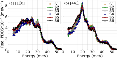
In Fig. 7 the Fe-partial reduced PDOS [g(E)/E2] of S1-S6 is shown. Along both directions no systematic increase in low-energy states is observed with reduction of from 24 nm (S1) to 10 nm (S3). However, the samples with the smallest NWs, S5 and S6, show an increase of states in the region from 5 to 15 meV. Such an enhancement of low-energy states has been observed in the PDOS of thin films Pradip et al. (2019); Fe3Si_interface ; Ślezak et al. (2007) and surfaces Stankov et al. (2007). It is attributed to interface/surface-specific vibrational modes, which are more pronounced in the smallest NWs.
A comparison of the PDOS and reduced PDOS of the capped and uncapped NWs of S3 and S4 unveils only minor deviations (see figure in supplementary material sm ). The negligible influence of the capping layer can be explained by the endotaxial growth of the NWs, which results in a large NW/substrate interface and a small fraction of atoms located at the surface of the NWs.
III.3 Thermodynamic and elastic properties
The thermodynamic and elastic properties obtained from the ab initio calculated and experimentally determined PDOS Chumakov and Sturhahn (1999) are given in Table 3. The experiments show an average decrease of the mean force constant by 1.6 % along [] compared to [], while the mean square displacement and the vibrational entropy on average increase by 5 % and 2 %, respectively. These differences originate from the vibrational anisotropy of the tetragonal -FeSi2 unit cell. The contribution of z-polarized phonons along -FeSi2[] induces the observed softening of the crystal compared to -FeSi2[].
The reduction of of the NWs from S1-S6 leads to an increase of by 5 % along [] and by 5.8 % along []. This is in agreement with the trend observed in the values obtained for the Fe-Si scattering path by modeling the EXAFS data (see Table. 2). is also slightly increased from S1 to S6, most likely due to the enhancement of high energy states above the cutoff energy, induced by the broadening of the peak at 45 meV. A similar behavior was observed in -FeSi2 nanoislands Kalt et al. (2020). A comparison with the theoretically expected values for bulk -FeSi2 shows that the and values are on average increased by 8 % and 2 %, respectively, in the smallest NWs. The values of the heat capacity coincide within the uncertainty for S1-S6 in both directions.
The low-energy part of the PDOS in all samples can be described by the Debye model: . The coefficient is on average increasing as the NWs size is decreasing (Fig. 7). Using , the sound velocity of S1-S6 was calculated Hu et al. (2003). For comparison the theoretical value for [], determined from the slopes of three acoustic branches calculated along -M direction, is also given. The experimental values are clearly reduced compared to the theoretical value. Reason for these differences is that a perfect crystal is assumed for the ab initio calculations, whereas in the NWs the propagation of sound waves is decelerated by scattering at defects, which are mostly present at interfaces. Since the interface-to-volume ratio is increased when the NWs dimensions are reduced, is also reduced from S1-S6 by 9 %.
IV Conclusions
Endotaxial FeSi2 NWs were grown on Si(110) by reactive deposition epitaxy. Systematic RHEED and AFM studies unveiled the formation of single-crystalline, unidirectionally aligned NWs with average widths from 24 to 3 nm and lengths from several m to about 100 nm. A combined experimental and theoretical EXAFS study demonstrated that the NWs exhibit the metastable, surface-stabilized -FeSi2 crystal structure.
The Fe-partial PDOS was determined along and across the NWs by NIS experiments performed at room temperature.
A pronounced vibrational anisotropy originating from the specific orientation of the tetragonal -FeSi2 unit cell on the Si(110) surface was unveiled.
Modeling of the experimental data with first-principles calculations showed that upon reduction of from 24 to 3 nm the features of PDOS broaden significantly.
This is attributed to phonon scattering at the NW/substrate interface, which is particularly strong in the smallest NWs characterized with the highest interface-to-volume ratio.
Furthermore, the reduction of from 24 nm to 3 nm leads to an increase of the mean square displacement by 5 % and a reduction of the sound velocity by 9 %.
The damping of lattice vibrations is slightly stronger across the nanowires, due to the smaller size of the -FeSi2 crystal along this direction.
A comparison of the PDOS of NWs with identical sizes measured with and without a capping layer demonstrates that the influence of surface-specific vibrational modes is negligible due to the endotaxial character of the NWs.
The presented results on the lattice dynamics and thermoelastic properties of FeSi2 nanowires are expected to be generally valid for the technologically important class of endotaxial silicide nanowires.
Acknowledgements.
S.S. acknowledges the financial support by the Helmholtz Association (VH-NG-625) and BMBF (05K16VK4). P.P. acknowledges support by the Narodowe Centrum Nauki (NCN, National Science Centre) under Project No. 2017/25/B/ST3/02586 and the access to ESRF financed by the Polish Ministry of Science and High Education, decision number: DIR/WK/2016/19. The European Synchrotron Radiation Facility is acknowledged for beamtime provision at the Nuclear Resonance beamline ID18. We thank Mr. J.-P. Celse for technical assistance during the experiment at ID18. We acknowledge DESY (Hamburg, Germany), a member of the Helmholtz Association HGF, for the provision of experimental facilities. Parts of this research were carried out at the High Resolution Dynamics Beamline P01 at PETRA III. We thank Mr. C. Hagemeister and Mr. F.-U. Dill for technical assistance during the experiment at P01.Literatur
- Murarka (1995) S.P. Murarka, Intermetallics 3, 173 (1995).
- Chen_book (2004) L.J. Chen, Silicide technology for integrated circuits Institution of Electrical Engineers, London (2004).
- Chen (2005) L.J. Chen, JOM 57, 24 (2005).
- Bennett et al. (2011) P.A. Bennett, Z. He, D.J. Smith, and F.M. Ross, Thin Solid Films 519, 8434 (2011).
- He et al. (2004) Z. He, D.J. Smith, and P.A. Bennett, Phys. Rev. Lett. 93, 256102 (2004).
- Mahato et al. (2017) J.C. Mahato, D. Das, N. Banu, B. Satpati, and B.N. Dev, Nanotechnology 28, 425603 (2017).
- Liang et al. (2006) S. Liang, R. Islam, D.J. Smith, P.A. Bennett, J.R. O’Brien, and B. Taylor, Appl. Phys. Lett. 88, 113111 (2006).
- Liang et al. (2006) S. Liang, R. Islam, D.J. Smith, and P.A. Bennett, J. Cryst. Growth 295, 166 (2006).
- Das et al. (2014) D. Das, J.C. Mahato, B. Bisi, B. Satpati, and B.N. Dev, Appl. Phys. Lett. 105, 191606 (2014).
- Zou et al. (2017) Z.-Q. Zou, X. Li, X.-Y. Liu, K.-J. Shi, and X.-Q. Guo, Appl. Surf. Sci. 399, 200 (2017).
- Bozyigit et al. (2016) D. Bozyigit, N. Yazdani, M. Yarema, O. Yarema, W.M.M. Li, S. Volk, K. Vuttivorakulchai, M. Luisier, F. Juranyi, and V. Wood, Nature 531, 618 (2016).
- Hepplestone (2005) S.P. Hepplestone, and G.P. Srivastava, Appl. Phys. Lett. 87, 231906 (2005).
- Steinhögl et al. (2002) W. Steinhögl, G. Schindler, G. Steinlesberger, and M. Engelhardt, Phys. Rev. B 66, 075414 (2002).
- Rideau et al. (2011) D. Rideau, W. Zhang, Y.M. Niquet, C. Delerue, C. Tavernier, and H. Jaouen, 2011 International Conference on Simulation of Semiconductor Processes and Devices 47 (2011).
- Tobler et al. (2015) S.K. Tobler, and P.A. Bennett, J. Appl. Phys. 118, 125305 (2015).
- Nishiguchi et al., (1997) N. Nishiguchi, Y. Ando, and M.N. Wybourne, J. Phys. Condens. Matter 9, 5751 (1997).
- Mukdadi et al., (1997) O.M. Mukdadi, S.K. Datta, and M.L. Dunn, J. Appl. Phys. 97, 074313 (2005).
- Srivastava (2006) S.P. Hepplestone and G.P. Srivastava, Nanotechnology 17, 3288 (2006).
- Allen (2007) P.B. Allen, Nano Lett. 7, 11 (2007).
- Mizuno et al., (2009) S. Mizuno and N. Nishiguchi, J. Phys. Condens. Matter 21, 195303 (2009).
- Sengün (2010) Y. Sȩngün and S. Durukanoǧlu, Phys. Rev. B 83, 113409 (2011).
- Velasco (2011) D. Martínez-Gutiérrez and V.R. Velasco, Surf. Sci. 605, 24 (2011).
- Mizuno (2014) S. Mizuno, Jpn. J. Appl. Phys. 53, 07KB02 (2014)Bessas.
- Saviot (2018) L. Saviot, Phys. Rev. B 97, 155420 (2018).
- Zou (2001) J. Zou and A. Balandin, J. Appl. Phys. 89, 2932 (2001).
- Glavin (2001) B.A. Glavin, Phys. Rev. Lett. 86, 4318 (2001).
- Lü (2006) X. Lü and J.H. Chu, J. Appl. Phys., 100, 014305 (2006).
- Qiu (2011) B. Qiu, L. Sun, and X. Ruan, Phys. Rev. B 83, 035312 (2011).
- Karamitaheri (2014) H. Karamitaheri, N. Neophytou, and H. Kosina, J. Appl. Phys. 115, 024302 (2014).
- Zhou (2017) Y. Zhou, X. Zhang, and M. Hu, Nano Lett. 17, 1269 (2017).
- Rashid (2018) Z. Rashid, L. Zhu, and Wu Li, Phys. Rev. B 97, 075441 (2018).
- Qiu (2011) B. Qiu and X. Ruan, Phys. Rev. B 83, 035312 (2011).
- Nishiguchi (2002) N. Nishiguchi, Physica E 13, 1 (2002).
- Uno (2011) S. Uno, J. Hattori, K. Nakazato, and M. Nobuya, J. Comput. Electron. 10, 104 (2011).
- Yamada (2012) Y. Yamada, H. Tsuchiya, and M. Ogawa, J. Appl. Phys. 111, 063720 (2012).
- Tienda-Luna (2013) I.M. Tienda-Luna, F.G. Ruiz, A. Godoy, L. Donetti, C. Martínez-Blanque, and F. Gámiz, Appl. Phys. Lett. 103, 163107 (2013).
- Malhotra (2019) A. Malhotra and M. Maldovan, Nanotechnology 30, 372002 (2019).
- Li et al. (1999) B. Li, D. Yu, and S.-L. Zhang, Phys. Rev. B 59, 1645 (1999).
- Wang et al. (2000) R.P. Wang, G.W. Zhou, Y.L. Liu, S.H. Pan, H.Z. Zhang, D.P. Yu, and Z. Zhang, Phys. Rev. B 61, 16827 (2000).
- Piscanec et al. (2003) S. Piscanec, M. Cantoro, A.C. Ferrari, J.A. Zapien, Y. Lifshitz, S.T. Lee, S. Hofmann, and J. Robertson, Phys. Rev. B 68, 241312(R) (2003).
- Adu et al. (2005) K.W. Adu, H.R. Gutierrez, U.J. Kim, G.U. Sumanasekera, and P.C. Eklund, Nano Lett. 5, 409 (2005).
- Patsha et al. (2018) A. Patsha and S. Dhara, Nano Lett. 18, 7181 (2018).
- Luca et al. (2019) M. De Luca, C. Fasolato, M.A. Verheijen, Y. Ren, M.Y. Swinkels, S. Kölling, E.P.A.M. Bakkers, R. Rurali, X. Cartoixa, and I. Zardo, Nano Lett. 19, 4702 (2019).
- Mante et al. (2018) P.-A. Mante, L. Belliard, and B. Perrin, Nanophotonics 7, 1759 (2018).
- Mariager et al. (2010) A.O. Mariager, D. Khakhulin, H.T. Lemke, K.S. Kjaer, L. Guerin, L. Nuccio, C.B. Sørensen, M.N. Nielsen, and R. Feidenhans’l, Nano Lett. 10, 2461 (2010).
- Kargar et al. (2016) F. Kargar, B. Debnath, J.-P. Kakko, A. Säynätjoki, H. Lipsanen, D.L. Nika, R.K. Lake, and A.A. Balandin, Nature Com. 7, 13400 (2016).
- Bessas et al. (2013) D. Bessas, W. Töllner, Z. Aabdin, N. Peranio, I. Sergueev, H.-C. Wille, O. Eibl, K. Nielsch, and R.P. Hermann, Nanoscale 5, 10629 (2013).
- Temstögl et al. (2019) D.P. Lozano, S. Couet, C. Petermann, G. Hamoir, J.K. Jochum, T. Picot, E. Menendez, K. Houben, V. Joly, V.A. Antohe, M.Y. Hu, B.M. Leu, A. Alatas, A.H. Said, S. Roelants, B. Partoens, M.V. Milosevic, F.M. Peeters, L. Piraux, J. Van de Vondel, A. Vantomme, K. Temst, and M.J. Van Bael, Phys. Rev. B 99, 064512 (2019).
- Krause et al. (2012) B. Krause, S. Darma, M. Kaufholz, H.-H. Gräfe, S. Ulrich, M. Mantilla, R. Weigel, S. Rembold, and T. Baumbach, J. Synchrotron Radiat. 19, 216 (2012).
- Ravel et al. (2005) B. Ravel and M. Newville, J. Synchrotron Radiat., 12 537 (2005.
- Kohn and Chumakov (2000) V.G. Kohn and A.I. Chumakov, Hyperfine Interact. 125, 205 (2000).
- (52) M. Seto, Y. Yoda, S. Kikuta, X.W. Zhang, and M. Ando, Phys. Rev. Lett. 74, 3828 (1995).
- (53) W. Sturhahn, T.S. Toellner, E.E. Alp, X. Zhang, M. Ando, Y. Yoda and S. Kikuta, M. Seto, C.W. Kimball, and B. Dabrowski , Phys. Rev. Lett. 74, 3832 (1995).
- Wille et al. (2010) H.-C. Wille, H. Franz, R. Röhlsberger, W.A. Caliebe, and F.U. Dill, J. Phys.: Conf. Series 217, 0120081 (2010).
- Rüffer and Chumakov (1996) R. Rüffer and A.I. Chumakov, Hyperfine Interact. 97, 589 (1996).
- Ibrahimkutty et al. (2015) S. Ibrahimkutty, A. Seiler, T. Prüßmann, T. Vitova, R. Pradip, O. Bauder, P. Wochner, A. Plech, T. Baumbach, and S. Stankov, J. Synchrotron Radiat. 22, 91 (2015).
- (57) G. Kresse and J. Furthmüller, Phys. Rev. B 54, 11169 (1996).
- (58) G. Kresse and J. Furthmüller, Comput. Mater. Sci. 6, 15 (1996).
- (59) J.P. Perdew, K. Burke, and M. Ernzerhof, Phys. Rev. Lett. 77, 3865 (1996).
- (60) J.P. Perdew, K. Burke, and M. Ernzerhof, Phys. Rev. Lett. 78, 1396 (1997).
- (61) K. Parlinski, Z.Q. Li, and Y. Kawazoe, Phys. Rev. Lett. 78, 4063 (1997).
- (62) K. Parlinski, Software PHONON ver. 6.15, Cracow, Poland, 2015.
- Kalt et al. (2020) J. Kalt, M. Sternik, B. Krause, I. Sergueev, M. Mikolasek, D. Bessas, O. Sikora, T. Vitova, J. Göttlicher, R. Steininger, P.T. Jochym, A. Ptok, O. Leupold, H.-C. Wille, A.I. Chumakov, P. Piekarz, K. Parlinski, T. Baumbach, and S. Stankov, Phys. Rev. B 101, 165406 (2020).
- (64) P. Delescluse and A. Masson, Surf. Sci. 100, 423 (1980).
- (65) P. J. Dobson, J.H. Neave and B.A. Joyce, Surf. Sci. 119, L339 (1982).
- (66) G. Wang, S.K. Lok, S.K. Chan, C. Wang, G.K.L. Wong and I.K. Sou, Nanotechnology 20, 215607 (2009).
- (67) See Supplemental Material at http for RHEED, EXAFS, AFM data evaluation, calculation of the direction-projected phonon density of states, and comparison of ex situ and in situ PDOS.
- Berbezier et al. (1994) I. Berbezier, J. Chevrier, and J. Derrien, Surf. Sci. 315, 27 (1994).
- Kataoka et al. (2006) K. Kataoka, K. Hattori, Y. Miyatake, and H. Daimon, Phys. Rev. B 74, 155406 (2006).
- Chumakov and Sturhahn (1999) A.I. Chumakov and W. Sturhahn, Hyperfine Interact. 123/124, 718 (1999).
- (71) S.Y. Chen, H.C. Chen, and L.J. Chen, Appl. Phys. Lett. 88 193114 (2006).
- (72) J.H. Won, K. Sato, M. Ishimaru, and Y. Hirotsu, J. Appl. Phys. 100, 014307 (2006).
- Chumakov et al. (1997) A.I. Chumakov, R. Rüffer, A.Q.R. Baron, H. Grünsteudel, H.F. Grünsteudel, and V.G. Kohn, Phys. Rev. B 56, 10758 (1997).
- Kohn et al. (1998) V.G. Kohn, A.I. Chumakov, and R. Rüffer, Phys. Rev. B 58, 8437 (1998).
- Fultz (2010) B. Fultz, Prog. Mater. Sci. 55, 247 (2010).
- (76) B. Fåk and B. Dorner, Institute Laue Langevin Technical Report No. 92FA008S, 1992, (unpublished); B. Fåk and B. Dorner, Physica B 234, 1107 (1997).
- (77) The experimental data was additionally modeled with Axy and Az being free parameters in the least squares optimization. The quality factors obtained with this approach coincide within the uncertainty with the values given in Fig. 5, Axy and Az deviate at most by 2 % from the calculated values of Axy=0.9 and Az=0.1.
- Pradip et al. (2019) R. Pradip, P. Piekarz, D.G. Merkel, J. Kalt, O. Waller, A.I. Chumakov, R. Rüffer, A.M. Oleś, K. Parlinski, T. Baumbach, and S. Stankov, Nanoscale 116, 10968 (2019).
- (79) J. Kalt, M. Sternik, I. Sergueev, J. Herfort, B. Jenichen, H.-C. Wille, O. Sikora, P. Piekarz, K. Parlinski, T. Baumbach, and S. Stankov, Phys. Rev. B 98, 121409(R) (2018).
- Ślezak et al. (2007) T. Ślezak, J. Łażewski, S. Stankov, K. Parlinski, R. Reitinger, M. Rennhofer, R. Rüffer, B. Sepiol, M. Ślezak, N. Spiridis, M. Zajac, A.I. Chumakov, and J. Korecki, Phys. Rev. Lett. 99, 0661031 (2007).
- Stankov et al. (2007) S. Stankov, R. Röhlsberger, T. Ślezak, M. Sladecek, B. Sepiol, G. Vogl, A.I. Chumakov, R. Rüffer, N. Spiridis, J. Łażewski, K. Parlinski,and J. Korecki, Phys. Rev. Lett. 99, 1855011 (2007).
- Hu et al. (2003) M.Y. Hu, W. Sturhahn, T.S. Toellner, P.D. Mannheim, D.E. Brown, J. Zhao, and E.E. Alp, Phys. Rev. B 67, 094304 (2003).