Ultrafast optical circuit switching for data centers
using integrated soliton microcombs
Abstract
Networks inside current data centers comprise a hierarchy of power-hungry electronic packet switches interconnected via optical fibers and transceivers. As the scaling of such electrically-switched networks approaches a plateau, a power-efficient solution is to implement a flat network with optical circuit switching (OCS), without electronic switches and a reduced number of transceivers due to direct links among servers. One of the promising ways of implementing OCS is by using tunable lasers and arrayed waveguide grating routers. Such an OCS-network can offer high bandwidth and low network latency, and the possibility of photonic integration results in an energy-efficient, compact, and scalable photonic data center network. To support dynamic data center workloads efficiently, it is critical to switch between wavelengths in sub nanoseconds (ns). Here we demonstrate ultrafast photonic circuit switching based on a microcomb. Using a photonic integrated microcomb in conjunction with semiconductor optical amplifiers (SOAs), sub ns (< 500 ps) switching of more than 20 carriers is achieved. Moreover, the 25-Gbps non-return to zero (NRZ) and 50-Gbps four-level pulse amplitude modulation (PAM-4) burst mode transmission systems are shown. Further, on-chip Indium phosphide (InP) based SOAs and arrayed waveguide grating (AWG) are used to show sub-ns switching along with 25-Gbps NRZ burst mode transmission providing a path toward a more scalable and energy-efficient wavelength-switched network for future data centers.
There is a massive growth in data center network traffic due to emerging applications such as AI, server-less computing, resource disaggregation, multimedia streaming, and big dataKatz (2009). These applications are evolving quite drastically, requiring data centers networks with low-latency, high-bandwidth, and high scalability. Current data center networks comprise a multi-tier interconnection of electronic switches and optical transceivers that consume a lot of power, particularly at high network bandwidths. Further, continued bandwidth scaling of the electrical switches poses a significant challengeBallani et al. (2018); Cheng et al. (2018).
Optical circuit switching (OCS) has been proposed as an alternative technology to overcome these challenges; it can provide high bandwidth and low network latency (due to no network buffers), and by allowing for a flat data center topology, the network can be more energy-efficient as fewer electrical switches and transceivers are requiredBarry et al. (2018). In OCS the servers are optically interconnected directly without needing the opto-electronic-opto (O-E-O) conversion. Micro-electro-mechanical (MEMS) based OCS systems are commercially available with the possibility of high port counts ( 1000 ports)Han et al. (2014); Kim et al. (2003). However, MEMS-based OCS architectures suffer from slow switching time ( ms), affecting efficient utilization of network resources, and require extreme fabrication precision. In contrast, modern data centers require fast switching ( ns) to efficiently support emerging hardware-accelerated applications; for applications like key-value stores, > 97% of the packets have a size of 576 bytes or lessClark et al. (2018). Many photonic chip-based techniques have been used to demonstrate the fast optical switching (ns) such as semiconductor optical amplifiers (SOAs) Tanaka et al. (2009), electro-absorption modulators (EAMs) Segawa et al. (2013), and Mach–Zehnder interferometers (MZIs)Dupuis et al. (2019, 2020). The arrayed waveguide grating routers (AWGRs) Yin et al. (2013); Xiao et al. , in conjunction with a tunable laser (TL), is a promising optical circuit switching technology as the core of the network is passive which benefits both fault-tolerance and future scaling. Recent studies have shown that the tuning of the laser plays a major role in switching speed, and it has been indeed improved from 80 ns to 5 ns by optimizing the designs Simsarian et al. (2006); Funnell et al. (2017). Moreover, sub-ns switching system is demonstrated recently by “disaggregating” or separating the lasing from the actual tuningShi et al. (2019); Ballani et al. (2020). This has been achieved, for example, by using a discrete bank of lasers as a multi-wavelength source and a wavelength selector containing photonic integrated arrayed waveguide grating (AWG) and SOAs. The SOAs are preferred as switching elements due to fast and lossless switching, chip-scale integration, and high extinction ratio Tanaka et al. (2009).
Here we propose and demonstrate in a proof-of-concept experiment a disaggregated tunable transceiver that uses photonic chip-based soliton microcombs as a multi-wavelength source, which are generated in high-quality () microresonators exhibiting third-order nonlinearity () and anomalous dispersionKippenberg et al. (2018); Herr et al. (2013). The soliton microcombs have been used in many system-level applications, for example, distance ranging (LiDAR) Trocha et al. (2018); Suh and Vahala (2018a); Riemensberger et al. , microwave photonics Torres-Company and Weiner (2014); Wu et al. (2018); Suh and Vahala (2018b); Liu et al. (2020a), optical coherence tomography (OCT) Ji et al. (2019); Marchand et al. (2020), and coherent communication Marin-Palomo et al. (2017); Fülöp et al. ; Corcoran et al. . The remarkable improvements in the losses of high-confinement integrated waveguides, a widely used platform for integrated photonics Moss et al. (2013); Blumenthal et al. (2018), allows the generation of solitons using the on-chip laser Stern et al. (2018); Pavlov et al. (2018); Raja et al. (2019). The broadband-bandwidth operation across C- and L-bands, precise spacing control to match ITU frequency grid (50/100 GHz), low power consumption, and wafer-scale scalability make the soliton microcomb an attractive solution for an ultra-fast wavelength switched system in comparison with a bank of lasers Marin-Palomo et al. (2017). Further, no extra guard band is required for frequency stabilization or to align each comb channel to the frequency grid.
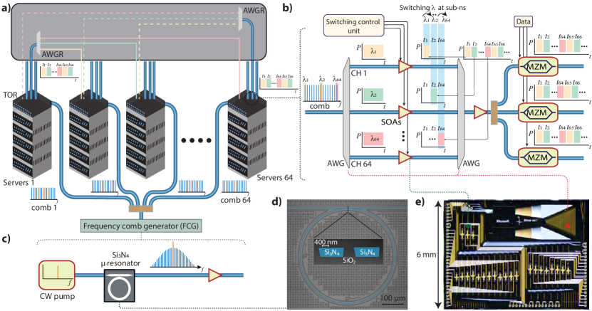
We use a based soliton microcomb as a multi-wavelength source to show ultrafast ( 550 ps) optical wavelength switching. In a proof-of-concept experiment, we demonstrate switching of 20 individual comb channels in a sub-ns time scale ( 550 ps) using discrete SOAs. Further, 25-GBd (baud-rate) no-return to zero on-off keying (NRZ) and four-level pulse amplitude modulation (PAM-4) burst mode transmission systems along with ultrafast switching are shown. Then, a more compact switching system consisting of PIC-based AWG and SOAs is implemented to show sub-ns switching and 25-GBd NRZ burst mode transmission, indicating the potential utilization of such a miniaturized system to mitigate power and scaling issues. A key advantage of the disaggregated transceiver design is that the multi-wavelength comb source can be shared across many (e.g. 64) servers in parallel instead of using 64 separate comb sources, using a split-and-amplify architecture (figure 1a). The source can thus be treated as a shared infrastructure element such as the power source in today’s data centers. This allows for an appealing division of functionality since the power consumed by the comb source is amortized as the power efficiency of the end-to-end system converges to the efficiency of the amplifiers while allowing for a high-quality and stable light source that can be rapidly wavelength-tuned (cf. discussion on power analysis and Supplementary information (SI)).
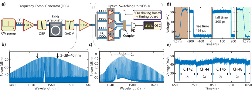
Figure 1 shows the OCS architecture containing the soliton microcomb, SOAs, AWGs in the switch and AWGRs to route the data across many servers (cf. Method). This architecture allows further parallelization of different resources by sharing the soliton across many servers and modulators for power efficiency and parallel data transmission, respectively (figure 1a & b ). The multi-wavelength source is generated by pumping a packaged microresonator fabricated using the photonic Damascene reflow Pfeiffer et al. (2018); Liu et al. (2018a) process enabling a mean intrinsic -factor () of > 15 million. Initially, a multi-soliton is initiated by performing a scan over resonance (forward tuning) and then a single soliton is generated via backwards switching Guo et al. (2017) (Figure 2b). The soliton is amplified using a low-noise and compact EDFA resulting in a comb with a maximum power of up to -4 dBm and an optical signal-to-noise ratio (OSNR) of > 34 dB. The post-amplified soliton as shown in figure 2c is de-multiplexed using a 100G spaced 48 channels AWG ( 1525 -1564 ) providing 30-dB isolation. The individual comb channels are initially switched using discrete SOAs with a small-signal gain 11-13 dB at 1550 nm. Figure 2d shows a 10% 90% rise and fall times of 493 ps and 395 ps, respectively, for a single microcomb carrier centered at 1555 nm (CH 37 of AWG) when applying a current of 120 mA to operate the SOA. Similarly, more than 20 comb channels (1540 - 1564 ) in C-band are tested individually to show sub-ns switching (cf. SI). Even though not tested due to the unavailability of an L-band AWG, the current results indicate that more than 40 comb channels in the L-band could be used as well.
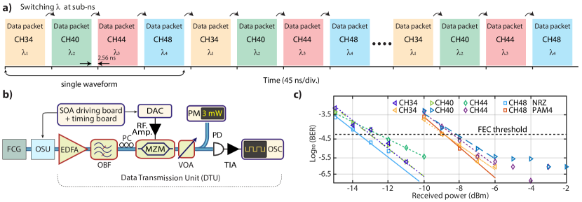
For a proof-of-concept system-level demonstration, fast switching within a four different comb channels is performed. Figure 2e shows 4 different comb channels switching at ns-timescale with a separation of 5.6 . A guard zone of 2.56 ns is used to allow a smooth switching between adjacent comb channels while an external reference clock (timing board) aligns the different switching signals. Distinct currents are applied to the SOAs to achieve a constant output power and to compensate for the non-uniform comb power per line or SOAs gain (figure 2e). While the sub-ns switching of four channels with a maximum 20 nm separation has been demonstrated, the maximum channel separation is mainly limited by the optical band-pass filter (cf. SI).
In the following experiment, we show 25 Gbps (NRZ) and 50 Gbps (PAM-4) burst mode data transmission while switching between four comb channels using the setup shown in figure 3b. The four optical carriers after switching are further amplified to overcome the insertion loss () of the 20-GHz Mach-Zehnder modulator (MZM) which is operating at the quadrature point. In addition to eliminating comb channels in the next order FSR of the AWG, the OBF is utilized to suppress the out-of-band SOA and EDFA amplified spontaneous emission (ASE) noise. The burst mode sequence at 25 GBaud symbol rate, generated by the arbitrary waveform generator is applied to the MZM with a random sequence of - and -bits for NRZ and PAM-4 respectively. The electrical waveform is amplified using a trans-impedance amplifier (TIA) after detecting it on a fast photodiode having 50-GHz bandwidth. The amplified waveform is acquired using a real-time oscilloscope with 160 GSamples/s sampling rate. The digital signal processing (DSP), explained in detail in ref Shi et al. (2019), is performed offline to obtain the bit error ratio (BER). The received optical power (ROP) vs. (BER) of the system, as shown in figure 3c, is characterized by changing the optical power of incoming waveform via a variable optical attenuator (VOA). A BER of below , which is the threshold for forward error correction (FEC) in data center transmission systems, is achieved for both NRZ and PAM-4 at a ROP of -12 dBm and -8 dBm respectively. The BER error floor for PAM4 at a ROP of > -6 dBm emerges due to ASE and AWG crosstalk.
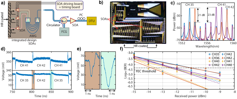
Next, integrated Indium phosphide (InP) chip-based SOAs and AWG are used to show 25-Gbps NRZ burst mode data transmission along with fast OCS using a soliton microcomb. Figure 4b shows the photonic integrated circuit (PIC) based wavelength selector PIC with a dimension of 6 mm 8 mm. The reflection of the light from the high-reflection (HR) coated facet allows simultaneous utilization of an AWG with 3250 GHz separated channels as multiplexer and de-multiplexer. This simplifies the wavelength alignment procedure and reduces the footprint of the device. Nineteen SOAs are connected via integrated waveguides to AWG output channels. The wavelength alignment of the comb channels to the AWG is performed by changing the temperature of the PIC, resulting in seven comb channels matching with the AWG. This can also be realized by changing the temperature of the chip. Figure 4c shows the optical spectrum of the AWG aligned comb channels indicating a >20 dB isolation with adjacent channels. Initially, the 10% 90% rising and falling times of PIC is characterized by performing simultaneous switching between two comb channels. The maximum (minimum) experimentally observed switching time is 820 ps ( 375 ps). Moreover, the overshoot in the switching signal, as seen in figure 4d, arises due to impedance mismatch between the SOAs on-chip electrodes and the RF probes Shi et al. (2019). Then, a burst mode data transmission demonstration with 25-Gbps NRZ modulation is performed. A BER below FEC threshold is obtained when switching between two-channels with different combinations for a ROP -11 dBm. The PAM-4 burst mode transmission demonstration requires further improvement in the output power of the comb due to low in- and out-coupling in a packaged . The main reason behind the low coupling efficiency (15 %) is an additional 2-dB splicing loss between UHNA and SMF-28 fiber, which can be reduced to 0.2 dB by using state-of-art splicing instrumentsYin et al. (2019). Similarly, the AWG crosstalk and insertion of loss of the PIC can be further improved to enhance the overall performance of this architecture. Nevertheless, the current results show the potential of a soliton microcomb as a suitable multi-wavelength source for 25 GBd NRZ burst mode transmission along with fast switching.
Regarding the power consumption, the current multi-wavelength source consumes a total electrical power of 30 W (cf. SI) providing more than 60 carriers, having an optical power -20 dBm ( 500 mW electrical power per carrier). The electrical power consumption can be improved down to 193 mW per carrier (15.5 W total) by reducing the splicing loss between UHNA and SMF fibers Yin et al. (2019), implementing on-chip actuators Liu et al. (2020b) instead of a bulk temperature controller and using a power-efficient, compact distributed feedback (DFB) laser as CW pump Stern et al. (2018); Raja et al. (2019). By optimizing the microresonator dispersion design, it is possible to generate 122 comb channels having an optical power > -14 dBm without needing any post-amplification Marin-Palomo et al. (2017). Similarly, an optimized amplifier utilization with an amplifier for C- and L-band, respectively, would give a comb with an optical power per line 13 dBm in the C- and L- bands mentioned in SI of ref. Marin-Palomo et al. (2017).
More importantly, this high power comb source can be shared among multiple servers by adding a hierarchy of passive optical splitters and amplifiers for better power and resource utilization (figure 1a). The soliton microcomb source distributed among 32 servers provides carriers with -4 dBm while consuming 2.57 W (1.115 W) electrical power per server by using a state of the art commercial EDFA (on-chip amplifier Juodawlkis et al. (2011)) making it a highly power-efficient and flexible solution for the data center (cf. SI). More broadly, the flexibility of sharing the comb across many servers, with the fast wavelength selection done on the server itself, means that the overall electrical power efficiency per channel approaches the power efficiency of the EDFAs with the comb power as only a small contributor. This indicates that an optimized shared comb source would consume a comparable electrical power to other multi-wavelength source solutions, including recent techniques that use a bank of tunable lasers as a multi-wavelength sourceGerard et al. (2020); Ballani et al. (2020). Since the wavelength tuning is done on the bank of tunable lasers itself, sharing it between multiple servers would lead to an increased complexity when synchronizing the wavelength switching between the servers, due to the varying time delays between the bank of tunable lasers and the servers. As a matter of fact, one tunable laser bank per server would be more optimal for a time-multiplexed solution Gerard et al. (2020) which would require at least 232 tunable lasers for switching between 32 servers instead of a single amplified comb chip. Moreover, a comb does not require additional complex algorithms for fast switching and wavelength stabilization, thus offering an appealing division of functionality by leveraging a complex yet highly shared light source.
In conclusion, ultrafast optical circuit switching is demonstrated using a chip-based microcomb for future power-efficient and low latency data centers. More than twenty individual comb channels in C-band having a power > -20 dBm have been switched at 550 ps using discrete SOAs. The optical circuit switching system with 25-GBd NRZ and PAM-4 burst mode data transmission is shown while switching between different comb channels. Further, a PIC containing on-chip SOAs and an AWG is implemented to show sub-ns switching and 25-GBd NRZ transmission. The current demonstration can provide a route for a fully integrated, fast-tunable transceiver providing dense carriers for wavelength switching to meet the power and latency requirements posed by future cloud workloads.
Methods
Switching architecture:
The link between two servers is only established via a single wavelength (comb tooth) in specific time slots () as shown in figure 1a. The soliton microcombs provide many coherent optical carriers assigned to distinct servers. The switching operation is performed by applying a control signal on the SOAs, e.g., the switching from to data slot is done by applying an on signal to the second SOA and off signals to all other SOAs. A trigger signal from an external reference clock is used to align the switching control and data-encoding units.
microresoantor: The microresonators are fabricated by using photonic Damascene reflow process enabling waveguides with ultra-smooth sidewalls and linear propagation loss 1 dB\m Pfeiffer et al. (2018); Liu et al. (2020a). The designed microresonators are over-coupled () with a FSR of 99.5 GHz and intrinsic linewidth of 15 MHz Liu et al. (2018a). The waveguides have a dimension of 1500900 . The double inverse nano tapers are used to facilitate the light coupling in- and out- of the chip Liu et al. (2018b).
Soliton microcomb generation: A compact fiber laser (Koheras BASIK) is amplified using an EDFA. Then, amplified spontaneous emission (ASE) noise is filtered out using a narrow optical bandpass filter. The chip is packaged by splicing the ultrahigh numerical aperture (UHNA) fiber with standard SMF-28 fiber with chip through (fiber-chip-fiber) 15% coupling efficiency Raja et al. (2020). A single soliton is initiated at an input power of 450 in the bus waveguide by applying a custom designed ramp voltage. The deterministic soliton initiation and backward tuning are controlled via a computer interface. The strong pump line is filtered out using an OADM. Then the soliton is amplified using a low-noise EDFA before de-multiplexing.
PIC: The InP-based wavelength selector PIC incorporates 23 SOAs of which 4 are used as references. The other 19 SOAs are connected to an 1x32 AWG which acts as a multiplexer and demultiplexer. One of the PIC facets is high-reflection coated so that the light is reflected back through the SOAs and AWG to the input waveguide. The reflective single AWG design reduces the footprint compared to using two AWGs and avoids wavelength misalignment of the AWGs. The wavelength selector PIC was designed using the JEPPIX foundry and fabricated at Fraunhofer HHI.
Switching control unit: The switching control unit provides the bias currents and electrical switching signals to the SOAs. It also controls the clock and time synchronisation of the switching signals.
Funding Information: This work was supported by a joint research ICES agreement no. MRL Contract No. 2019-034 (01.01.2019 - 31.12.2021). This material is based upon work supported by the Air Force Office of Scientific Research, Air Force Materiel Command, USAF under Award No. FA9550-19-1-0250, and by Swiss National Science Foundation under grant agreement No. 176563 (BRIDGE). This work was supported by funding from the European Union H2020 research and innovation programme PhoMEC under grant agreement 862528.
Acknowledgments:
The samples were fabricated and grown in the Center of MicroNanoTechnology (CMi) at EPFL.
Author contribution: A.L. and K.S. designed the and InP samples, respectively. J.L. fabricated the microresonator. A.S.R., S.L., and M.K. characterized the samples. M.K., X.F., and A.S.R. contributed in breadboard based soliton generator. S.L., A.S.R., and K. S. carried out switching communication experiments. R.B., D.C., I.H., F.K., B.T. and K.J. contributed in the optical transmission system design and optimization. K.S., S.L., and A.S.R. analysed and processed the data. A.S.R., S.L., H.B., and T.J.K. wrote the manuscript, with the input from others. H.B., T.J.K., and P.C. supervised the project.
Data Availability Statement: The code and data used to produce the plots within this work will be released on the repository Zenodo upon publication of this preprint.
References
- Katz (2009) R. H. Katz, IEEE Spectrum 46, 40 (2009).
- Ballani et al. (2018) H. Ballani, P. Costa, I. Haller, K. Jozwik, K. Shi, B. Thomsen, and H. Williams, in Optical Fiber Communication Conference (OSA, 2018) p. W1C.3.
- Cheng et al. (2018) Q. Cheng, M. Bahadori, M. Glick, S. Rumley, and K. Bergman, Optica 5, 1354 (2018).
- Barry et al. (2018) L. P. Barry, J. Wang, C. McArdle, and D. Kilper, in Optical Switching in Next Generation Data Centers, edited by F. Testa and L. Pavesi (Springer International Publishing, 2018) pp. 23–44.
- Han et al. (2014) S. Han, T. J. Seok, N. Quack, B.-w. Yoo, and M. C. Wu, in Optical Fiber Communication Conference (2014), paper M2K.2 (Optical Society of America, 2014) p. M2K.2.
- Kim et al. (2003) J. Kim, C. Nuzman, B. Kumar, D. Lieuwen, J. Kraus, A. Weiss, C. Lichtenwalner, A. Papazian, R. Frahm, N. Basavanhally, D. Ramsey, V. Aksyuk, F. Pardo, M. Simon, V. Lifton, H. Chan, M. Haueis, A. Gasparyan, H. Shea, S. Arney, C. Bolle, P. Kolodner, R. Ryf, D. Neilson, and J. Gates, IEEE Photonics Technology Letters 15, 1537 (2003).
- Clark et al. (2018) K. Clark, H. Ballani, P. Bayvel, D. Cletheroe, T. Gerard, I. Haller, K. Jozwik, K. Shi, B. Thomsen, P. Watts, H. Williams, G. Zervas, P. Costa, and Z. Liu, in 2018 European Conference on Optical Communication (ECOC) (2018) pp. 1–3.
- Tanaka et al. (2009) S. Tanaka, S.-H. Jeong, S. Yamazaki, A. Uetake, S. Tomabechi, M. Ekawa, and K. Morito, IEEE Journal of Quantum Electronics 45, 1155 (2009).
- Segawa et al. (2013) T. Segawa, M. Nada, M. Nakamura, Y. Suzaki, and R. Takahashi, in 39th European Conference and Exhibition on Optical Communication (ECOC 2013) (2013) pp. 1–3.
- Dupuis et al. (2019) N. Dupuis, J. E. Proesel, H. Ainspan, C. W. Baks, M. Meghelli, and B. G. Lee, Optics Letters 44, 3610 (2019).
- Dupuis et al. (2020) N. Dupuis, J. E. Proesel, N. Boyer, H. Ainspan, C. W. Baks, F. Doany, E. Cyr, and B. G. Lee, in Optical Fiber Communication Conference Postdeadline Papers 2020 (2020), paper Th4A.6 (Optical Society of America, 2020) p. Th4A.6.
- Yin et al. (2013) Y. Yin, R. Proietti, X. Ye, C. J. Nitta, V. Akella, and S. J. B. Yoo, IEEE Journal of Selected Topics in Quantum Electronics 19, 3600409 (2013).
- (13) X. Xiao, Y. Zhang, K. Zhang, R. Proietti, and S. J. B. Yoo, in 2019 Conference on Lasers and Electro-Optics (CLEO), pp. 1–2.
- Simsarian et al. (2006) J. Simsarian, M. Larson, H. Garrett, H. Xu, and T. Strand, IEEE Photonics Technology Letters 18, 565 (2006).
- Funnell et al. (2017) A. C. Funnell, K. Shi, P. Costa, P. Watts, H. Ballani, and B. C. Thomsen, Journal of Lightwave Technology 35, 4438 (2017).
- Shi et al. (2019) K. Shi, S. Lange, I. Haller, D. Cletheroe, R. Behrendt, B. Thomsen, F. Karinou, K. Jozwik, P. Costa, and H. Ballani, in The 45th European Conference on Optical Communication (ECOC Post-deadline Paper) (2019).
- Ballani et al. (2020) H. Ballani, P. Costa, R. Behrendt, D. Cletheroe, I. Haller, K. Jozwik, F. Karinou, S. Lange, K. Shi, B. Thomsen, and H. Williams, Proceedings of ACM SIGCOMM, (2020).
- Kippenberg et al. (2018) T. J. Kippenberg, A. L. Gaeta, M. Lipson, and M. L. Gorodetsky, Science 361 (2018).
- Herr et al. (2013) T. Herr, V. Brasch, J. D. Jost, C. Y. Wang, N. M. Kondratiev, M. L. Gorodetsky, and T. J. Kippenberg, Nature Photonics 8, 145 (2013).
- Trocha et al. (2018) P. Trocha, M. Karpov, D. Ganin, M. H. P. Pfeiffer, A. Kordts, S. Wolf, J. Krockenberger, P. Marin-Palomo, C. Weimann, S. Randel, W. Freude, T. J. Kippenberg, and C. Koos, Science 359, 887 (2018).
- Suh and Vahala (2018a) M.-G. Suh and K. J. Vahala, Science 359, 884 (2018a).
- (22) J. Riemensberger, A. Lukashchuk, M. Karpov, W. Weng, E. Lucas, J. Liu, and T. J. Kippenberg, Nature 581, 164.
- Torres-Company and Weiner (2014) V. Torres-Company and A. M. Weiner, Laser & Photonics Reviews 8, 368 (2014).
- Wu et al. (2018) J. Wu, X. Xu, T. G. Nguyen, S. T. Chu, B. E. Little, R. Morandotti, A. Mitchell, and D. J. Moss, IEEE Journal of Selected Topics in Quantum Electronics 24, 1 (2018).
- Suh and Vahala (2018b) M.-G. Suh and K. Vahala, Optica 5, 65 (2018b).
- Liu et al. (2020a) J. Liu, E. Lucas, A. S. Raja, J. He, J. Riemensberger, R. N. Wang, M. Karpov, H. Guo, R. Bouchand, and T. J. Kippenberg, Nature Photonics 14, 486 (2020a).
- Ji et al. (2019) X. Ji, X. Yao, A. Klenner, Y. Gan, A. L. Gaeta, C. P. Hendon, and M. Lipson, Optics Express 27, 19896 (2019).
- Marchand et al. (2020) P. J. Marchand, J. C. Skehan, J. Riemensberger, J.-J. Ho, M. H. P. Pfeiffer, J. Liu, C. Hauger, T. Lasser, and T. J. Kippenberg, arXiv:1902.06985 [physics] (2020).
- Marin-Palomo et al. (2017) P. Marin-Palomo, J. N. Kemal, M. Karpov, A. Kordts, J. Pfeifle, M. H. P. Pfeiffer, P. Trocha, S. Wolf, V. Brasch, M. H. Anderson, R. Rosenberger, K. Vijayan, W. Freude, T. J. Kippenberg, and C. Koos, Nature 546, 274 (2017).
- (30) A. Fülöp, M. Mazur, A. Lorences-Riesgo, s. B. Helgason, P.-H. Wang, Y. Xuan, D. E. Leaird, M. Qi, P. A. Andrekson, A. M. Weiner, and V. Torres-Company, Nature Communications 9, 1598.
- (31) B. Corcoran, M. Tan, X. Xu, A. Boes, J. Wu, T. G. Nguyen, S. T. Chu, B. E. Little, R. Morandotti, A. Mitchell, and D. J. Moss, Nature Communications 11, 2568.
- Moss et al. (2013) D. J. Moss, R. Morandotti, A. L. Gaeta, and M. Lipson, Nature Photonics 7, 597 (2013).
- Blumenthal et al. (2018) D. J. Blumenthal, R. Heideman, D. Geuzebroek, A. Leinse, and C. Roeloffzen, Proceedings of the IEEE, Proceedings of the IEEE 106, 2209 (2018).
- Stern et al. (2018) B. Stern, X. Ji, Y. Okawachi, A. L. Gaeta, and M. Lipson, Nature 562, 401 (2018).
- Pavlov et al. (2018) N. G. Pavlov, S. Koptyaev, G. V. Lihachev, A. S. Voloshin, A. S. Gorodnitskiy, M. V. Ryabko, S. V. Polonsky, and M. L. Gorodetsky, Nature Photonics 12, 694 (2018).
- Raja et al. (2019) A. S. Raja, A. S. Voloshin, H. Guo, S. E. Agafonova, J. Liu, A. S. Gorodnitskiy, M. Karpov, N. G. Pavlov, E. Lucas, R. R. Galiev, A. E. Shitikov, J. D. Jost, M. L. Gorodetsky, and T. J. Kippenberg, Nature Communications 10, 1 (2019).
- Pfeiffer et al. (2018) M. H. P. Pfeiffer, J. Liu, A. S. Raja, T. Morais, B. Ghadiani, and T. J. Kippenberg, Optica 5, 884 (2018).
- Liu et al. (2018a) J. Liu, A. S. Raja, M. Karpov, B. Ghadiani, M. H. P. Pfeiffer, B. Du, N. J. Engelsen, H. Guo, M. Zervas, and T. J. Kippenberg, Optica 5, 1347 (2018a).
- Guo et al. (2017) H. Guo, M. Karpov, E. Lucas, A. Kordts, M. H. P. Pfeiffer, V. Brasch, G. Lihachev, V. E. Lobanov, M. L. Gorodetsky, and T. J. Kippenberg, Nature Physics 13, 94 (2017).
- Yin et al. (2019) P. Yin, J. R. Serafini, Z. Su, R.-J. Shiue, E. Timurdogan, M. L. Fanto, M. L. Fanto, and S. Preble, Optics Express 27, 24188 (2019).
- Liu et al. (2020b) J. Liu, H. Tian, E. Lucas, A. S. Raja, G. Lihachev, R. N. Wang, J. He, T. Liu, M. H. Anderson, W. Weng, S. A. Bhave, and T. J. Kippenberg, Nature 583, 385 (2020b).
- Juodawlkis et al. (2011) P. W. Juodawlkis, J. J. Plant, W. Loh, L. J. Missaggia, F. J. O’Donnell, D. C. Oakley, A. Napoleone, J. Klamkin, J. T. Gopinath, D. J. Ripin, S. Gee, P. J. Delfyett, and J. P. Donnelly, IEEE Journal of Selected Topics in Quantum Electronics 17, 1698 (2011).
- Gerard et al. (2020) T. Gerard, C. Parsonson, Z. Shabka, P. Bayvel, D. Lavery, and G. Zervas, arXiv:2003.05489 [cs, eess] (2020).
- Liu et al. (2018b) J. Liu, A. S. Raja, M. H. P. Pfeiffer, C. Herkommer, H. Guo, M. Zervas, M. Geiselmann, and T. J. Kippenberg, Optics Letters 43, 3200 (2018b).
- Raja et al. (2020) A. S. Raja, J. Liu, N. Volet, R. N. Wang, J. He, E. Lucas, R. Bouchandand, P. Morton, J. Bowers, and T. J. Kippenberg, Optics Express 28, 2714 (2020).