[SI-]SI_MnPS3_domain_v092920
Ultrafast current and field driven domain-wall dynamics in van der Waals antiferromagnet MnPS3
Abstract
The discovery of magnetism in two-dimensional (2D) van der Waals (vdW) materials[1, 2, 3, 4] has flourished a new endeavour of fundamental problems in magnetism as well as potential applications in computing, sensing and storage technologies[5, 6, 7, 8, 9, 10]. Of particular interest are antiferromagnets [11, 12], which due to their intrinsic antiferromagnetic exchange coupling show several advantages in relation to ferromagnets such as robustness against external magnetic perturbations. This property is one of the cornerstones of antiferromagnets[13] and implies that information stored in antiferromagnetic domains is invisible to applied magnetic fields preventing it from being erased or manipulated. Here we show that, despite this fundamental understanding, the magnetic domains of recently discovered 2D vdW MnPS3 antiferromagnet[14, 15] can be controlled via external magnetic fields and electric currents. We realize ultrafast domain-wall dynamics with velocities up to 1500 m s-1 and 3000 m s-1 respectively to a broad range of field magnitudes (0.000122 T) and current densities ( A cm-2). Both domain wall dynamics are determined by the edge terminations which generated uncompensated spins following the underlying symmetry of the honeycomb structure. We find that edge atoms belonging to different magnetic sublattices function as geometrical constrictions preventing the displacement of the wall, whereas having atoms of the same sublattice at both edges of the material allows for the field-driven domain wall motion which is only limited by the spin-flop transition of the antiferromagnet beyond 25 T. Conversely, electric currents can induce motion of domain walls in most of the edges except those where the two sublattices are present at the borders (e.g. armchair edges). Furthermore, the orientation of the layer relative to the current flow provides an additional degree of freedom for controlling and manipulating magnetic domains in MnPS3. Our results indicate that the implementation of 2D vdW antiferromagnets in real applications requires the engineering of the layer edges which enables an unprecedented functional feature in ultrathin device platforms.
School of Mathematics and Physics, Queen’s University Belfast, BT7 1NN, UK
Department of Physics, The University of York, YO10 5DD, UK
Department of Material Science & Engineering, National University of Singapore, Block EA, 9 Engineering Drive 1, 117575, Singapore
Chongqing 2D Materials Institute, Liangjiang New Area, Chongqing 400714, China
Institute for Condensed Matter Physics and Complex Systems, School of Physics and Astronomy, The University of Edinburgh, EH9 3FD, UK
†email: esantos@ed.ac.uk
The emergence of magnetism in 2D vdW materials has opened exciting new avenues in the exploration of spin-based applications at the ultimate level of few-atom-thick layers. Remarkable properties including giant tunnelling magnetoresistance[16, 17, 4] and layer stacking dependent magnetic phase[18, 19] have recently been demonstrated. Even though these studies show that rich physical phenomena can be observed in 2D ferromagnets, the dynamics of domain walls which determine whether such compounds can be effectively implemented in real life device platforms remains elusive. Very few reports have shed some light on the intriguing behaviour of magnetic domains[20, 21] and their walls[22] in ferromagnetic layered materials. The scenario is even less clear for 2D antiferromagnets where the antiferromagnetic exchange coupling between spins adds a level of complexity in terms of the manipulation of the magnetic moments by conventional techniques as zero net magnetization is obtained[13]. Indeed, recent measurements using tunnelling magnetoresistance, a common approach for ferromagnetic materials, unveiled that antiferromagnetic correlations persist down to the level of individual monolayers of MnPS3[23]. This result suggests that yet unexplored ingredients at low dimensionality play an important role in the detection and manipulation of the antiferromagnetic order in 2D vdW compounds. Moreover, how domain walls in MnPS3 behave and can be controlled externally in functional devices for practical applications are still open questions.
Here we show that electrical currents and, unexpectedly, magnetic fields can move domain walls in monolayer MnPS3 at low-temperatures achieving fast velocities within the km s-1 limit. While bulk antiferromagnetic compounds are insensitive to magnetic fields, the interplay between low-dimensionality and edge-type offers control over domain wall dynamics via an initially unthinkable external parameter. In configurations where the layer terminates with either a zigzag array of Mn atoms or dangling-bonds, the domain walls are controllable via both currents and magnetic fields at a broad range of magnitudes. For configurations where the edge atoms assume an armchair configuration, the domain wall appears pinned and no motion is observed irrespective of the field intensity or current density applied. Our results indicate a rich variety of possibilities depending on the edge roughness and introduces the layer termination as one of the determinant factors for integration of 2D antiferromagnets in novel domain-wall based applications.
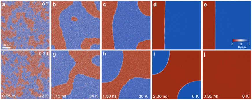
We firstly investigate how magnetic domains are formed in monolayer MnPS3 through simulating the zero-field cooling process for a large square flake of 0.3 m 0.3 m using atomistic spin dynamics which incorporate atomistic (several Å’s) and micromagnetic (m-level) underlying details (see full set of details in Supplementary Notes LABEL:SI-methods-dftLABEL:SI-LLG1). The system is thermally equilibrated above the Curie temperature at 80 K and then linearly cooled to 0 K in a simulated time of 4.0 ns as shown in Figure 1 and Supplementary Movies S1-S2. The time evolution of the easy-axis component of the magnetization Sz is used to display the nucleation of the magnetic domains at different temperatures and magnetic fields. While domain walls appeared at zero field with a large extension over the simulation area (Fig. 1a-e), an external field can flush out any domains resulting in a homogeneous magnetization after 2 ns (Fig. 1f-j). We also observed that some simulations at zero field ended up in the formation of a monodomain throughout the surface. This suggests that antiferromagnetic domains are not intrinsically stable in MnPS3 similarly as in ferromagnetic layered materials, e.g. CrI3[22]. Indeed, the metastability of the domains prevents the wall profiles from reaching a truly ground-state configuration as they initially appears winded with several nodes at 0 K (Fig. 1d), but incidentally evolved to an unwound state (Fig. 1e). A close look reveals a continuous rotation of the spins over the extension of the wall pushing the nodes out of the domain wall profile (Supplementary Figure LABEL:SI-wind-DW and Supplementary Movie S3). Such interactions between nodes can extend as long as 95 nm along the wall which is more that two order of magnitudes larger than the thickness (0.8 nm[14]) of the monolayer MnPS3. At longer times, the domain wall reaches stability and does not show any sudden variations on the spin configurations.
To determine whether the interplay between metastability and the high magnetic anisotropy of MnPS3 could give additional features to the domain walls, we analyse the local behaviour of the spins in the domain wall (Figure 2). We notice that as the spins rotate from one magnetic domain to another they tend to align with the zig-zag crystallographic direction displaying an angle of (Fig. 2a-b). The projections of the total magnetization at the wall over the out-of-plane (Sz) and in-plane (Sx, Sy) components show sizeable magnitudes of Sy and Sx as the spins transition from one domain to another despite the easy-axis anisotropy along of Sz (Fig. 2c-d). This indicates a domain wall of hybrid characteristics rather than one of Bloch and Néel type (Fig. 2e-f). We can extract the domain wall width by fitting the different components of the magnetization (Sx, Sy, Sz) to standard equations[24] of the form:
| (1) | |||||
| (2) |
where and z0 are the domain wall positions at in-plane and out-of-plane coordinates, respectively. The domain wall widths are within the range of nm. Such small widths are commonly observed in permanent magnetic materials[24] due to their exceptionally high magnetic anisotropy such as Nd2Fe14B (3.9 nm), SmCo5 (2.6 nm), CoPt (4.5 nm) and Mn overlayers on Fe(001) (4.55 nm)[25]. In these systems, magnetic domains are energetically stable after zero-field cooling due to long range dipole interactions which were also checked in our study resulting in no modifications of the results. Therefore, MnPS3 reunites characteristics from soft-magnets (large area uniform magnetization) and hard-magnets (large magnetic anisotropy, narrow domain walls) within the same material.
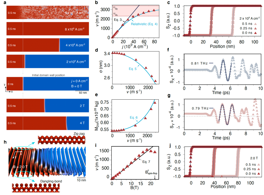
An outstanding question raised by these hybrid features is whether the domain walls can be manipulated by electric currents and magnetic fields. It is well known that antiferromagnets are insensitive to external magnetic fields but are rather controllable through currents particularly in high-anisotropy materials[13, 26]. However, the low dimensionality together with the underlying symmetry of the honeycomb structure may lead to novel features on the dynamics of domain walls not yet observed in bulk antiferromagnets. To investigate this we simulate the spin-transfer torque induced by spin-polarized currents and the effect of magnetic fields on a large nano-flake of monolayer MnPS3 of dimensions of 300 nm50 nm (see Supplementary Note LABEL:SI-torque for details). The domain wall is initially stabilized from one-atom-thick wall which broadens and develops a profile during the thermalization over a simulation time of 0.5 ns. The system is then allowed to evolve for longer times ( ns) to ensure that no changes are observed in the system close to the end of the dynamics.
Surprisingly, both electric currents and magnetic fields are able to induce the motion of domain walls in the antiferromagnetic MnPS3 resulting in a broad range of velocities (Figure 3). For current-induced domain wall motion, wall velocities up to 3000 m s-1 are seen at a maximum current density of A cm-2 (Fig. 3a-b). At such large values of , we observe primarily two regimes that are characterized by different dependences of with . For 109 A cm-2 (Fig. 3b) a linear dependence is noticed which can be described by a one-dimensional model (Supplementary Note LABEL:SI-sec:1D-model) as:
| (3) |
where , with the Bohr magneton, the domain wall width, the spin Hall angle, the Gilbert damping parameter, the electron charge, the modulus of the magnetization per lattice, and the layer thickness. Eq.3 is consistent with adiabatic spin-transfer mechanisms in thin antiferromagnets[13, 26, 27] where the conduction electrons from the current transfer angular momentum to the spins of the wall which keeps its coherence through a steady motion (Fig. 3a and Supplementary Movie S4). The value of extracted from our simulation data helps to find other parameters not easily accessible in experiments or from theory, e.g. . The magnitude of determines the conversion efficiency between charge and spin currents, and it is the figure of merit of any spintronic application. Using the definition of (Supplementary Note LABEL:SI-sec:1D-model), we can estimate which is comparable to standard heterostructures and antiferromagnets[13] but at a much thinner limit. This suggests MnPS3 as a potential layered compound for power-efficient device platforms. For 109 A cm-2 the wall velocities tend to saturate to a maximum magnitude near 3000 m s-1 (Fig. 3b) with a deviation from the linear dependence observed previously (Eq. 3). This intriguing behaviour can be understood in terms of the relativistic kinematics of antiferromagnets[28, 13]. As the wall velocities approach the maximum group velocities (, ), which sets the maximum speed for spin interactions into the system, relativistic effects in terms of the Lorenz invariance become more predominant. This is due to the finite inertial mass of the antiferromagnetic domain wall which can be decomposed into spin-waves represented through relativistic wave equations[28, 29, 27]. We can extend this idea further in a 2D vdW antiferromagnet by examining the variations of several quantities via special relativity concepts. For instance, the variation of the wall velocities versus current densities can be well analysed using:
| (4) |
where is the maximum spin-wave group velocity at one of the branches of the magnon dispersion (Supplementary Note LABEL:SI-sec:magnon). Eq.4 includes quasi-relativistic corrections[29, 27] to the linear dependence recorded at low values of the density (Eq. 3) and can be solved self-consistently in for each magnitude of . Strikingly, Eq.4 provides an accurate description of the wall velocity not only at low magnitudes of the density, where relativistic effects are rather small, but also for 109 A cm-2. At such limit, the domain wall width and the domain wall mass MDW also shrinks and expands, respectively, exhibiting effects similar to the Lorentz contraction (Fig. 3d-e). These phenomena can be reasoned by (see Supplementary Note LABEL:SI-sec:1D-model for details):
| (5) | |||||
| (6) |
where is domain wall width at low-velocities (3.41 nm), (with the exchange parameter for the first nearest-neighbours and the gyromagnetic ratio), is the width of the stripe of the material, and is the layer thickness. There is a sound agreement between the simulation data (Fig. 3d-e) and Eqs. 56 over a wide range of velocities with minor deviations occurring above 2500 m s-1 due to non-linear spin excitations. We found that at such large wall velocities, spin waves or magnons are emitted throughout the layer with frequencies in the terahertz regime (Fig. 3f-g). These excitations can be found in the wake of the wall forming simultaneously in front and behind the wall motion (see Supplementary Movie S5). Analysing the variations of Sz over time at different (Supplementary Figure LABEL:SI-turbulent-DW), we noticed that high currents generated precession of the spins around the easy-axis with their high in-plane projections (Sx, Sy) being transmitted through spin-waves into the system (Fig. 3f-g). This is critical at large values of where the variation of the position of the domain wall with time results in two velocities before and after the magnons start being excited (Supplementary Figure LABEL:SI-turbulent-DW). This behaviour is particularly turbulent at longer times as the wall profile can not be defined any more with the appearance of several vortex, antivortex and spin textures at both edges of the layer and inside the flake (Supplementary Movie S6).
To have a deeper understanding of the characteristics of spin excitations on the domain wall dynamics in MnPS3, we have developed an analytical model using linear spin-wave theory[30, 31] that accounts on the magnon dispersion ) and their group velocities over the entire Brillouin zone. Supplementary Note LABEL:SI-sec:magnon provides a full description of the details involved. The maximum spin-wave group velocities (, ) that MnPS3 can sustain at different magnon branches (Supplementary Figure LABEL:SI-group-vel) are in the range from m s-1 to m s-1 (Fig. 3b). These magnitudes correspond to the highest velocities at which spin excitations can propagate in the system and put the lower () and upper limits () where magnons participate in the domain-wall dynamics. Indeed, there is a good agreement with the numerically calculated wall-velocities where the spin-waves start being emitted into the sheet (2248 m s-1), and the wall saturates to its maximum speed (2970 m s-1). The slightly lower values obtained in the simulations relative to and are due to the effect of damping on the propagation of domain walls due to the emission of spin-waves. A similar feature has been observed in the past in 3D ferromagnetic[32, 33] and antiferromagnetic[27, 34] compounds but the emergence of such phenomena in a 2D vdW antiferromagnet is unprecedented. Additionally, we can estimate a maximum wave frequency () corresponding to of about 4.03 THz. This value surpasses those measured in the state-of-the-art antiferromagnetic materials such as in MnO[35], NiO[36, 37], DyFeO3[38], HoFeO3[39] and heterostructures combining MnF2 and platinum[40] by several times. This implies that antiferromagnetic domain walls in MnPS3 can be used as a terahertz source of electric signal at the ultimate limit of a few atoms thick layer.
Remarkably, the application of a magnetic field results in a very counter-intuitive behaviour as the domain wall moves with velocities as high as 1500 m s-1 (Fig. 3h-j and Supplementary Note LABEL:SI-sec:field_dw for additional discussions). We can fit most of the field-induced domain wall dynamics for T with:
| (7) |
with a linear regression coefficient of . The motion is steady, keeping the wall shape throughout the motion. We observe however that both the domain wall width and the domain wall mass change their magnitudes in opposite trend as that observed in the current-driven domain wall dynamics (Supplementary Figure LABEL:SI-width_mass_B). We attribute this difference to the distinct operation of the external stimulus on the domain wall. In the current driven case, the action is tightly focused at the centre of the wall, where the angular change in neighbouring spins is the largest. For large currents the wall is not able to relax fully leading to relativistic contraction in the wall width. In contrast, the magnetic field acts across the whole wall and tends to strengthen the spin flop (SF) state, which in turn leads to an increase in the domain wall width with increasing field strength (Supplementary Figure LABEL:SI-width_mass_Ba). This effect is sufficient to counteract the relativistic effect (which is also present) and leads to a net decrease of the domain wall mass (Supplementary Figure LABEL:SI-width_mass_Bb). Wider domain walls naturally have lower mass as they are easier to move until SF states are achieved for fields above 22 T. In addition, some curvature is formed as the wall moves with its starting points from the terminations of the sheet parallel to the wall movement (Fig. 3a, h and Supplementary Movie 7). The spins around one edge move in advance relative to those at the middle of the system and at the opposite edge creating a curved wall during the motion (see detailed features in Supplementary Movie 8). Such deviation from the planar wall shape has been reported in hetero-interfaces formed by NiFe/FeMn bilayers[41] but not yet in a monolayer of a 2D vdW antiferromagnet. This indicates a direct relation between domain-wall motion and the material geometry via edge roughness similarly as in magnetic wires[42]. A close look unveils that the type of edge plays a pivotal role in the domain wall dynamics induced by both magnetic fields and electric currents. Sheets terminated with edge atoms in zig-zag (ZZ) and dangling-bond (DB) configurations (Fig. 3h) in any combination (e.g. ZZ-ZZ, ZZ-DB, DB-DB) are susceptible to be manipulated by currents. Nevertheless, only domain wall in layers with dissimilar edges (e.g. ZZ-DB) can be controlled by magnetic fields. Borders formed by atoms in the armchair (ARM) configuration remain inert irrespective of the stimulus applied (Supplementary Figure LABEL:SI-arm1). Intriguingly, ARM edges under applied currents show a short displacement of the domain wall at earlier stages of the dynamics (0.07 ns) but rapidly stabilizes to a constant position at longer times. As the current flows through the wall, the spins feel the torque induced by the spin-polarized electrons but rather than reorient the spins to follow the current direction, the spins at the wall precess around the easy-axis with no motion of the domain-wall. This mechanism is shown in details in Supplementary Movies S9-S10. The ARM edge in this case works as an effective pinning barrier for domain-wall propagation.
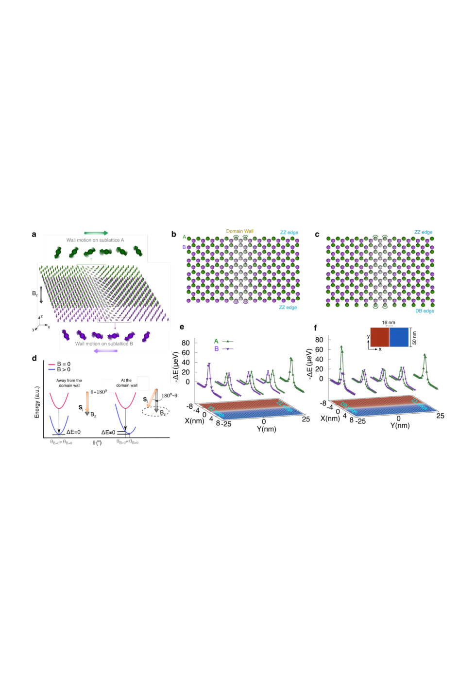
The control of the domain-wall motion in an antiferromagnetic material via magnetic fields opens a new ground in the investigation of the role of edges on 2D magnetic materials. The fundamental ingredient that enables such phenomena is based on the underlying magnetic sublattices (e.g. A or B) composing the honeycomb structure (Fig. 4a-c). Despite the border considered, for edge atoms residing at different sublattices the magnetic field induces a torque at each sublattice that mutually compensates each other generating no net displacement of the domain-wall (Supplementary Movie S11). For edge atoms at the same sublattice the effect is additive inducing the translation of the wall. Indeed, we can further confirm this mechanism analysing the spin interactions present in the system on a basis of a generalized XXZ Heisenberg Hamiltonian in the form of:
| (8) |
where is the bilinear exchange interactions between spins Si and Sj at sites and , is the anisotropic exchange, is the on-site magnetic anisotropy and Bi is the external magnetic field applied along the easy-axis (e.g. Bz). We only include bilinear exchange terms in Eq. 8 since biquadratic exchange interactions are negligible in MnPS3[43]. We considered pair-wise interactions in up to the third nearest neighbours () (Supplementary Table LABEL:SI-tbl:table2). All parameters are calculated using strongly correlated density functional theory based on Hubbard- methods. Supplementary Notes LABEL:SI-methods-dftLABEL:SI-mag-parameters convey the full details of the approaches employed. Eq. 8 is then applied to calculate the spin interactions into the system taking into account any angular variations of the spins induced by the field. We determine the stability of the system before and after the application of Bz distinguishing the atoms away from the domain wall from those at the wall (Fig. 4d). Such procedure is instrumental to unveil the influence of the edges on the energetics of the domain-wall dynamics as the atoms at these two spatial regions may respond differently to a magnetic perturbation. In fact, we found that spins that are distanced from the domain-wall (i.e. spin-up for , and spin-down for ) do not suffer any angular variation with Bz as the layer reached a new ground-state. Nevertheless, for spins at the domain-wall the new ground-state under a finite field (B) is obtained at a value of different to that at B (Fig. 4d-f). This indicates that the wall spins tend to rotate under magnetic fields and the effect is particularly strong for atoms at the edges. The variations in energy show that when the two edges are similar (Fig. 4e) two different sublattices will be localized at the borders which will respond likewise generating similar variation of energies. As the atoms at the edges are more uncoordinated relative to those in the bulk of the system, they gain more energy from aligning with Bz which allows the spins to rotate more freely but in opposite direction compensating any displacement of the domain-wall. The scenario is completely different when the atoms at the edges belong to the same sublattice such as in a ZZ-DB layer (Fig. 4f). In this case, has a larger variation at the DB edge due to the lesser coordination with neighbouring atoms and consequently less exchange energy. This results in a more prompt rotation of the spins at the DB edge than that at the ZZ edge dragging the wall slightly ahead with the field (Supplementary Movie S8). Even though our analysis has been applied for MnPS3 it should be universal for any antiferromagnetic layered material with a honeycomb lattice.
One of the main implications for having uncompensated spins at the edges selectively controlling domain-wall motion in 2D vdW antiferromagnets is that depending how the layer is oriented in a device-platform we can have many possibilities to induce domain wall dynamics. By engineering the type of edges in MnPS3 we can either induce a fast domain-wall dynamics through both current and magnetic fields, or no motion whatsoever via geometrical constrictions. Our findings suggest that 2D layered antiferromagnets would not be invisible to common magnetic probes (e.g. tunnelling magneto-resistance[23]) which is normally problematic for materials that hold antiferromagnetic coupling between the spins within the layer. In this case the antiferromagnetic layer can play a more active role in magnetic structures rather than induce exchange bias in an adjacent ferromagnetic layer[13]. With the rapid integration of magnetic layered materials in applications and the discovery of more compounds with similar characteristics, our predictions will open novel grounds in the investigations of edge-mediated 2D antiferromagnetic spintronics
Supplementary Materials
Supplementary Notes 115, Supplementary Movies 113 and Supplementary Figures 116.
Data Availability
The data that support the findings of this study are available within the paper and its Supplementary Information.
Competing interests
The Authors declare no conflict of interests.
Acknowledgments
RFLE gratefully acknowledges the financial support of ARCHER UK National Supercomputing Service via the embedded CSE programme (ecse1307). EJGS acknowledges computational resources through the UK Materials and Molecular Modelling Hub for access to THOMAS supercluster, which is partially funded by EPSRC (EP/P020194/1); CIRRUS Tier-2 HPC Service (ec131 Cirrus Project) at EPCC (http://www.cirrus.ac.uk) funded by the University of Edinburgh and EPSRC (EP/P020267/1); ARCHER UK National Supercomputing Service (http://www.archer.ac.uk) via Project d429. EJGS acknowledges the EPSRC Early Career Fellowship (EP/T021578/1) and the University of Edinburgh for funding support.
Author Contributions
EJGS conceived the idea and supervised the project. IMA performed ab initio and Monte Carlo simulations under the supervision of EJGS. IMA and EJGS elaborated the analysis and figures. RFLE implemented the spin-transfer-torque method. EJGS wrote the paper with inputs from all authors. KSN helped in the analysis and discussions. All authors contributed to this work, read the manuscript, discussed the results, and agreed to the contents of the manuscript.
References and Notes
References
- [1] Huang, B. et al. Layer-dependent ferromagnetism in a van der waals crystal down to the monolayer limit. Nature 546, 270 EP – (2017). URL https://doi.org/10.1038/nature22391.
- [2] Gong, C. et al. Discovery of intrinsic ferromagnetism in two-dimensional van der waals crystals. Nature 546, 265–269 (2017). URL http://dx.doi.org/10.1038/nature22060. Letter.
- [3] Guguchia, Z. et al. Magnetism in semiconducting molybdenum dichalcogenides. Science Advances 4 (2018). URL https://advances.sciencemag.org/content/4/12/eaat3672. https://advances.sciencemag.org/content/4/12/eaat3672.full.pdf.
- [4] Klein, D. R. et al. Probing magnetism in 2d van der waals crystalline insulators via electron tunneling. Science 360, 1218–1222 (2018). URL http://science.sciencemag.org/content/360/6394/1218. http://science.sciencemag.org/content/360/6394/1218.full.pdf.
- [5] Gibertini, M., Koperski, M., Morpurgo, A. F. & Novoselov, K. S. Magnetic 2d materials and heterostructures. Nature Nanotechnology 14, 408–419 (2019). URL https://doi.org/10.1038/s41565-019-0438-6.
- [6] Gong, C. & Zhang, X. Two-dimensional magnetic crystals and emergent heterostructure devices. Science 363 (2019). URL https://science.sciencemag.org/content/363/6428/eaav4450. https://science.sciencemag.org/content/363/6428/eaav4450.full.pdf.
- [7] Li, L. H., Tian, T., Cai, Q., Shih, C.-J. & Santos, E. J. G. Asymmetric electric field screening in van der waals heterostructures. Nature Communications 9, 1271 (2018). URL https://doi.org/10.1038/s41467-018-03592-3.
- [8] Santos, E. J. G. Carrier-mediated magnetoelectric coupling in functionalized graphene. ACS Nano 7, 9927–9932 (2013). URL https://doi.org/10.1021/nn4037877.
- [9] Hong, J. et al. Intrinsic controllable magnetism of graphene grown on fe. The Journal of Physical Chemistry C 123, 26870–26876 (2019). URL https://doi.org/10.1021/acs.jpcc.9b05886.
- [10] Tian, T. et al. Electronic polarizability as the fundamental variable in the dielectric properties of two-dimensional materials. Nano Letters 20, 841–851 (2020). URL https://doi.org/10.1021/acs.nanolett.9b02982.
- [11] Okuda, K. et al. Magnetic properties of layered compound mnps3. Journal of the Physical Society of Japan 55, 4456–4463 (1986). URL https://doi.org/10.1143/JPSJ.55.4456. https://doi.org/10.1143/JPSJ.55.4456.
- [12] Makimura, C., Sekine, T., Tanokura, Y. & Kurosawa, K. Raman scattering in the two-dimensional antiferromagnet MnPSe3. Journal of Physics: Condensed Matter 5, 623–632 (1993). URL https://doi.org/10.1088%2F0953-8984%2F5%2F5%2F013.
- [13] Baltz, V. et al. Antiferromagnetic spintronics. Rev. Mod. Phys. 90, 015005 (2018). URL https://link.aps.org/doi/10.1103/RevModPhys.90.015005.
- [14] Long, G. et al. Isolation and characterization of few-layer manganese thiophosphite. ACS Nano 11, 11330–11336 (2017). URL https://doi.org/10.1021/acsnano.7b05856.
- [15] Kim, K. et al. Antiferromagnetic ordering in van der waals 2d magnetic material MnPS3 probed by raman spectroscopy. 2D Materials 6, 041001 (2019). URL https://doi.org/10.1088%2F2053-1583%2Fab27d5.
- [16] Song, T. et al. Giant tunneling magnetoresistance in spin-filter van der waals heterostructures. Science 360, 1214–1218 (2018). URL http://science.sciencemag.org/content/360/6394/1214. http://science.sciencemag.org/content/360/6394/1214.full.pdf.
- [17] Wang, Z. et al. Very large tunneling magnetoresistance in layered magnetic semiconductor CrI3. Nat. Commun. 9, 2516 (2018).
- [18] Song, T. et al. Switching 2d magnetic states via pressure tuning of layer stacking. Nature Materials 18, 1298–1302 (2019). URL https://doi.org/10.1038/s41563-019-0505-2.
- [19] Chen, W. et al. Direct observation of van der waals stacking–dependent interlayer magnetism. Science 366, 983–987 (2019). URL https://science.sciencemag.org/content/366/6468/983. https://science.sciencemag.org/content/366/6468/983.full.pdf.
- [20] Thiel, L. et al. Probing magnetism in 2d materials at the nanoscale with single-spin microscopy. Science (2019). URL https://science.sciencemag.org/content/early/2019/04/24/science.aav6926. https://science.sciencemag.org/content/early/2019/04/24/science.aav6926.full.pdf.
- [21] Zhong, D. et al. Layer-resolved magnetic proximity effect in van der waals heterostructures. Nature Nanotechnology 15, 187–191 (2020). URL https://doi.org/10.1038/s41565-019-0629-1.
- [22] Wahab, D. A. et al. Quantum rescaling, metastability and hybrid domain-walls in two-dimensional cri3 magnets. arXiv: (2020).
- [23] Long, G. et al. Persistence of magnetism in atomically thin mnps3 crystals. Nano Letters 20, 2452–2459 (2020). URL https://doi.org/10.1021/acs.nanolett.9b05165.
- [24] Hubert, A. & Schafer, R. Magnetic Domains: The Analysis of Magnetic Microstructures (Springer Science and Business Media, 2008).
- [25] Schlickum, U., Janke-Gilman, N., Wulfhekel, W. & Kirschner, J. Step-induced frustration of antiferromagnetic order in mn on fe(001). Phys. Rev. Lett. 92, 107203 (2004). URL https://link.aps.org/doi/10.1103/PhysRevLett.92.107203.
- [26] Jungwirth, T., Marti, X., Wadley, P. & Wunderlich, J. Antiferromagnetic spintronics. Nature Nanotechnology 11, 231–241 (2016). URL https://doi.org/10.1038/nnano.2016.18.
- [27] Shiino, T. et al. Antiferromagnetic domain wall motion driven by spin-orbit torques. Phys. Rev. Lett. 117, 087203 (2016). URL https://link.aps.org/doi/10.1103/PhysRevLett.117.087203.
- [28] Haldane, F. D. M. Nonlinear field theory of large-spin heisenberg antiferromagnets: Semiclassically quantized solitons of the one-dimensional easy-axis néel state. Phys. Rev. Lett. 50, 1153–1156 (1983). URL https://link.aps.org/doi/10.1103/PhysRevLett.50.1153.
- [29] Kim, S. K., Tserkovnyak, Y. & Tchernyshyov, O. Propulsion of a domain wall in an antiferromagnet by magnons. Phys. Rev. B 90, 104406 (2014). URL https://link.aps.org/doi/10.1103/PhysRevB.90.104406.
- [30] Oguchi, T. Theory of spin-wave interactions in ferro- and antiferromagnetism. Phys. Rev. 117, 117–123 (1960). URL https://link.aps.org/doi/10.1103/PhysRev.117.117.
- [31] Kubo, R. The spin-wave theory of antiferromagnetics. Phys. Rev. 87, 568–580 (1952). URL https://link.aps.org/doi/10.1103/PhysRev.87.568.
- [32] Wieser, R., Vedmedenko, E. Y. & Wiesendanger, R. Domain wall motion damped by the emission of spin waves. Phys. Rev. B 81, 024405 (2010). URL https://link.aps.org/doi/10.1103/PhysRevB.81.024405.
- [33] Bouzidi, D. & Suhl, H. Motion of a bloch domain wall. Phys. Rev. Lett. 65, 2587–2590 (1990). URL https://link.aps.org/doi/10.1103/PhysRevLett.65.2587.
- [34] Tveten, E. G., Qaiumzadeh, A. & Brataas, A. Antiferromagnetic domain wall motion induced by spin waves. Phys. Rev. Lett. 112, 147204 (2014). URL https://link.aps.org/doi/10.1103/PhysRevLett.112.147204.
- [35] Nishitani, J., Nagashima, T. & Hangyo, M. Terahertz radiation from antiferromagnetic mno excited by optical laser pulses. Applied Physics Letters 103, 081907 (2013). URL https://doi.org/10.1063/1.4819181.
- [36] Kampfrath, T. et al. Coherent terahertz control of antiferromagnetic spin waves. Nature Photonics 5, 31–34 (2011). URL https://doi.org/10.1038/nphoton.2010.259.
- [37] Satoh, T. et al. Spin oscillations in antiferromagnetic nio triggered by circularly polarized light. Phys. Rev. Lett. 105, 077402 (2010). URL https://link.aps.org/doi/10.1103/PhysRevLett.105.077402.
- [38] Kimel, A. V. et al. Ultrafast non-thermal control of magnetization by instantaneous photomagnetic pulses. Nature 435, 655–657 (2005). URL https://doi.org/10.1038/nature03564.
- [39] Mukai, Y., Hirori, H., Yamamoto, T., Kageyama, H. & Tanaka, K. Antiferromagnetic resonance excitation by terahertz magnetic field resonantly enhanced with split ring resonator. Applied Physics Letters 105, 022410 (2014). URL https://doi.org/10.1063/1.4890475.
- [40] Vaidya, P. et al. Subterahertz spin pumping from an insulating antiferromagnet. Science 368, 160 (2020). URL http://science.sciencemag.org/content/368/6487/160.abstract.
- [41] Nikitenko, V. I. et al. Asymmetry in elementary events of magnetization reversal in a ferromagnetic/antiferromagnetic bilayer. Phys. Rev. Lett. 84, 765–768 (2000). URL https://link.aps.org/doi/10.1103/PhysRevLett.84.765.
- [42] Nakatani, Y., Thiaville, A. & Miltat, J. Faster magnetic walls in rough wires. Nature Materials 2, 521–523 (2003). URL https://doi.org/10.1038/nmat931.
- [43] Kartsev, A. et al. Higher-order exchange interactions in two-dimensional magnets. arXiv: (2020).
Figure captions