Optical Signatures of Defect Centres in Transition Metal Dichalcogenide Monolayers
Abstract
Even the best quality 2D materials have non-negligible concentrations of vacancies and impurities. It is critical to understand and quantify how defects change intrinsic properties, and use this knowledge to generate functionality. This challenge can be addressed by employing many-body perturbation theory to obtain the optical absorption spectra of defected transition metal dichalcogenides. Herein metal vacancies, which are largely unreported, show a larger set of polarized exitons than chalcogenide vacancies, introducing localized excitons in the sub-optical-gap region, whose wave functions and spectra make them good candidates as quantum emitters. Despite the strong interaction with substitutional defects, the spin texture and pristine exciton energies are preserved, enabling grafting and patterning in optical detectors, as the full optical-gap region remains available. A redistribution of excitonic weight between the A and B excitons is visible in both cases and may allow the quantification of the defect concentration. This work establishes excitonic signatures to characterize defects in 2D materials and highlights vacancies as qubit candidates for quantum computing.
keywords:
Optical absorption, Transition metal dichalcogenides, defect centres, quantum dotsPedro Miguel M. C. de Melo* Zeila Zanolli* Matthieu J. Verstraete
Dr. Pedro Miguel Monteiro Campos de Melo
nanomat/Q-mat/CESAM, Université de Liège, Institut de Physique, B-4000 Sart Tilman, Liège, Belgium
Chemistry Department, Debye Institute for Nanomaterials Science, Condensed Matter and Interfaces, Utrecht University, PO Box 80.000, 3508 TA Utrecht, The Netherlands
European Theoretical Spectroscopy Facility (ETSF) www.etsf.eu
Email: p.m.monteirocamposdemelo@uu.nl
Prof. Dr. Zeila Zanolli
Catalan Institute of Nanoscience and Nanotechnology (ICN2), CSIC and BIST, Campus UAB, Bellaterra, 08193 Barcelona, Spain
Chemistry Department, Debye Institute for Nanomaterials Science, Condensed Matter and Interfaces, Utrecht University, PO Box 80.000, 3508 TA Utrecht, The Netherlands
European Theoretical Spectroscopy Facility (ETSF) www.etsf.eu
Email: z.zanolli@uu.nl
Prof. Dr. Matthieu Jean Verstraete
nanomat/Q-mat/CESAM, Université de Liège, Institut de Physique, B-4000 Sart Tilman, Liège, Belgium
European Theoretical Spectroscopy Facility (ETSF) www.etsf.eu
Transition metal dichalcogenides (TMDs) have become strong contenders for the engineering of optical devices, especially thanks to their coupling of the spin and valley degrees of freedom, and the presence of strongly bound excitons, opening avenues for next generation opto-electronics1, 2. Manufactured samples have strongly improved in quality, but will always contain a significant concentration of defects3, 4. Graphene can be crystallized almost perfectly in very large flakes, but TMDs present many more natural defects, in particular chalcogen vacancies (see e.g. Ref. 5). On the bright side, defects and substitutional dopants can be used to tune the electronic structure and optical properties of materials 6. By doing so, devices sensitive to specific wavelengths and polarizations can be engineered (reviewed in Ref. 7), and can even behave as single photon emitters 8. There is an ongoing search for long lived spin states at room temperatures in TMDs. Here defects are expected to play a crucial role in both scattering and storing spin information - we showed recently that intrinsic scattering mechanisms (the electron-phonon interaction) can quickly destroy the pumped spin-polarisation 9. Chalcogen vacancies can also be used as grafting sites for functional groups, to create bio and chemical sensors10, 11. Alkane and other functional groups can be incorporated directly into the matrix (as opposed to thiol links, for instance, which necessitate Au). Carbon atoms have also been used as acceptor dopants for bulk semiconductors 12. In TMDs, mixed phases with transition metal carbides have been shown to have applications in catalysis 13, 14, while in MoS2 it was shown that carbon substitutions had a strong effect on the TMD electronic and optical properties 15, 16.
Many experiments give access to the presence and properties of localized defects. In TMDs the most commonly used are: Scanning Tunnelling Microscopy which shows contrast changes due to chemical substitution and electron cloud reconstruction around defects17; Scanning Tunnelling Spectroscopy, which probes the detailed electronic structure at the defect site17; optical spectroscopy showing absorption and photoluminescence by the defect-induced states18, 19, 20; tunnelling transport from insulated contacts through a core material, which is resonant through defect states in the core band gap19; transmission electron microscopy, which gives both structural and chemical information3, 21.
Understanding how defects affect optical properties is a first essential step towards controlled functionalization of materials, both for fingerprinting (optical characterization is simple, remote, and non destructive) and to understand derived optical functionalities. First-principles computational techniques provide a high degree of physical insight and predictive power in the spectral features of defects, to find new peaks and yield quantitative positions and weight transfers.
In this work, we present a fully First-principles investigation of defected monolayers of WS2, based on the Bethe Salpeter Equation (BSE) for electron-hole interactions within many body perturbation theory. We analyze the resulting changes in electronic band structure and optical absorption spectra, aiming to answer the question: can we identify a defect, and ideally quantify its concentration 22, just by looking at the absorption spectrum? While chalcogenide vacancies have been subject to some studies22, metal vacancies and isovalent substitutions like MoW and are still largely unreported, limiting our knowledge of their behaviour as quantum emitters or chemical detectors. We find that defects fall into two functional categories, based on the presence of bound states within the band-gap of WS2. We discuss their spectra, spin textures and the criteria which could be used to identify each defect.
In Figure 1 we show the four defects that are the focus of our work: two vacancies (S and W ions); and two substitutions, MoW and . The S vacancy is the most commonly found defect in monolayers of WS2 and often assigned to specific features below the optical gap 18. In the substitution case MoW is quite commonly found in nature, and carbon is a common dopant in semiconductors 23. Studies have been made on the potential transport applications of TMDs and transition metal carbides 13, 24. In the case of MoS2 experiments point to changes to the electronic structure due to carbon doping, which should translate into new optical features 15, 25.
In ideal defect engineering, induced changes in the system should yield new controllable features that are distinct from the pristine properties. In the case of TMDs, a key property that relates to optics is the polarisation of states at the K wave vector in the Brillouin zone. The polarization will control the allowed optical transitions that form bright excitons. We label in order of increasing energy the last two occupied states and the first two unoccupied states at K as . For pristine WS2 (see the Supplementary Material for more information), the first bright exciton would be made of an optical transition from to , while the second brightest exciton would be made by a transition from to . This is due to the fact that optical selection rules enforce spin conservation in TMDs: the valence and conduction manifold differ in orbital character, guaranteeing the needed angular momentum change when absorbing a helical photon 26.
We start by analyzing two systems which feature states in the pristine band gap: the sulfur and tungsten vacancies. Their DFT band structures are shown in Figure 1 a) and 1 c), respectively. Note that using a 55 supercell, the point K of the pristine Brillouin zone (BZ) folds back into the point K of the supercell BZ.
Both systems preserve the spin polarisation of pristine states at K, meaning that the A and B peaks that are the dominant features of the pristine spectrum must also be present. For the S vacancy, Figure 1 a), new non-dispersive mid-gap singlet states appear 1.08 and 1.28 eV above the valence band edge, in agreement with what was previously found 27, 16. At K the first band is almost completely spin-unpolarized, while the second is completely polarized. This opens a path for new emission channels, as electronic transitions from the pristine valence states to these new defect states are allowed, with different oscillator strengths and different excitation energies.
The W vacancy is more challenging numerically: the defect bands are split off from the bulk conduction and valence bands, but in the 55 supercell they still show some dispersion and a finite band width. Their position and spin texture are close to what has been found in other DFT calculations for this defect using larger supercells 16, and we extract a semi-quantitative picture of the optical properties. Together with the six new mid-gap states, there are also four new occupied states bound to the defect in the valence region (unlike the S vacancy). All these states are spin polarized at K, so if we consider optical selection rules, we can expect new peaks to show up in the absorption spectrum. These peaks will be a combination of transitions between pristine and defect states, and others between defect states (occupied to empty) in the mid-gap region.
The effects of changes in the band structure on the BSE optical spectrum are shown in Figure 3. For comparison the absorption spectrum of the pristine system is shown in grey. The energies of all identified excitons are listed in Table 1 in the SI, along with the reference energies for the pristine case. Note in passing that the higher energy peaks beyond A and B are not reproduced in full in our calculations, due to limitations in the number of states included in the BSE for such large systems.
With an S vacancy in Figure 1 a) two new peaks arise at 1.35 and 1.14 eV due to the mid-gap states. They are marked D1 and D2 in Figure 1 b). As shown in the inset, D1 and D2 correspond to optical transitions from the top valence band to the defect state at 1.28 eV and 1.08 eV, respectively. However, since the lowest defect state is not fully polarized, the resulting dipole matrix element is much smaller than that of the D1 peak, where the defect state is fully polarized.
The exciton wave function for the peak corresponding to D1 is shown in Figure 3 a). Here the hole is placed at the position of the vacant sulfur ion (marked by the green sphere) and the magnitude on the colour-map shows the probability density of the electron (see the Figure 5 in the SI where all the excitonic wave functions are depicted). The color map shows that exciton states are highly localized on the neighboring tungsten atoms, indicating that the S vacancy does indeed form a quantum dot.
For the W vacancy, whose spectrum is shown in Figure 1 d), more peaks are present due to the increased number of defect states. In total we identify five excitons: three composed from holes in the valence band and electrons in defect states, D1 to D3; and two others with both the electron and the hole bound to two different manifolds of defect states, D4 and D5. The states involved in the formation in the excitons are shown in the inset of Fig 1 d). The most striking feature is the relative intensity of the D4 and D5 excitons relative to the A and B excitons. As defect states have very weak dispersion, the associated electrons and holes will have large effective masses. It is possible to show 28 that oscillator strengths are proportional to the reduced mass of electron and hole, which explains why the effect is further magnified for transitions between defect states in the case of the W vacancy.
A more detailed analysis to the excitonic wave functions shows that two of the low intensity peaks (D1 and D3) are artefacts due to the interaction of defect states in neighboring periodic replicas. They result from electron-hole pairs localized on different vacancy sites (see Figure 7 in the SI for zoomed out plots of excitonic wave function). The majority of the electronic charge in the exciton is not localized near the same ion vacancy as the hole, and is bound thanks to a finite overlap of the DFT defect state wavefunctions. These two peaks will disappear if larger supercells are used: the dipole matrix element and oscillator strength will go do 0. We note that while the BSE is solved only for , the introduction of non-dispersive defect states allows for many transitions to occur throughout the BZ, so an exciton function can actually be composed of several vertical transitions at different momenta (NB: this is distinct from a finite wave vector for the whole exciton).
In the case of D2, shown in Figure 7 in the SI, there is a residual interaction with adjacent vacancy sites, but now the hole is correctly bound to an electron located at the same site. For D5, shown in Figure 3 b) both the electron and hole are entirely located at the same site.
We studied two cases of substitutions in the WS2 monolayer; one with a molybdenum atom replacing a tungsten atom; and another where a sulfur atom was replaced by a methyl, the simplest (divalent) group representing grafted organic substituents.
In both cases no mid gap states where found (see Figure 4 in the SI for their bandstructures), which can be rationalized as follows. In the case of MoW substitution, molybdenum and tungsten have the same valence, close atomic and covalent radii29, 30, 31, resulting in similar chemical properties. A small concentration of defects does not lead to strong changes in the charge density, thus leaving the system practically unchanged when compared to the pristine case. For the substitution, the methylene group provides the same number of valence electrons as the sulfur atom. The breaking of local symmetry is not strong enough to perturb the band edges.
The lack of mid-gap states is reflected in the absorption spectra shown in Figure 4. In both cases the excitonic peaks lie almost on top of those of the pristine system, with the largest deviation being 60 meV for the MoW A peak. The energies for the defected A and B peaks are shown in Table 1 in the SI.
There is, however, both weight transfer and changes in spin texture for the A and B peaks at higher energies in the absorption spectrum of both substitutions, which suggests methods to identify these defects experimentally. The strongest signature of the substitution lies within the exciton wave functions shown in Figure 5. While the exciton cloud is still dispersed throughout the crystal, there is a higher charge concentration near the substitution. In the case this is valid for the A exciton (Figure 5 c)), and in MoW both A and B excitonic states localize near the defect. The case also shows breaking of symmetry by the methyl molecule. The localization is due both to the defect-related electronic states and to the choice of the initial position of the hole. For reference, in boron nitride similar extensions of 3-5 nearest neighbors are found in Ref. 32.
The two peaks which correspond to the bulk excitons A and B known from literature, and are within 50 meV of those of the pristine system in all cases (this is below the absolute precision of the first principles methods, and shows the basic convergence of our supercell sizes).
We can now establish a more complete picture of how different defects change optical properties of TMDs. The main changes to the optical spectrum come from new mid-gap states. Isovalent substitutions like MoW and will not be trivially seen in the absorption spectra, but can still be detected by the ratio of the A and B peak intensities, and by localisation in the exciton’s spatial distribution.
In terms of potential applications, the two vacancies are clear front runners for designing quantum dots and quantum emitters. In particular the S vacancy has already shown some promising results as a single photon emitter 33. The two mid-gap defect states are actively considered for quantum computing applications: they are separated in energy by 0.21 eV, making them addressable using mid-infrared lasers, and insulating them from the highest phonon energy in pristine WS2, which is 53 meV 34, 35.
The W vacancy offers a larger set of localized excitons, but is more energetic and harder to produce (see Table 1 in the SI). Here the brightest excitons are made of transitions between single particle defect states, due to their large effective masses. These exciton states show potential in devices as they would behave as bright emitters with multiple internal states, behaving like an embedded molecule for multivalued quantum computing36. The residual band width will disappear only in a 77 supercell16, but the spin texture and qualitative features are already well represented here (see Figure 3 in the SI). In actual samples, this vacancy type is more likely to be charged, with electrons filling the dangling S ion’s orbitals.
We have shown that the isovalent substitutions MoW and will not produce in-gap states. Though this is intuitive, it is not trivial, and the local electronic structure is strongly modified as shown by the excitonic wave functions. For purposes of grafting organic molecules, this means the full band gap window of intrinsic WS2 will be available for optical sensing.
In conclusion, we employ powerful and accurate first principles techniques to shed some light into the changes in optical properties introduced by point defects in TMDs. Two promising systems, S and W ion vacancies, have potential for quantum emitters and even quantum computing. Isovalent vacancies do not introduce mid-gap states in the band structure, but do change the relative intensity of the canonical A and B peaks, and the spatial distribution of the first and second excitonic states, in the case even leading to a breaking of symmetry. In both cases the full sub optical gap region is available for use in detection of molecules that might graft themselves onto the TMD’s surface.
Supporting Information
Supporting Information is available from the Wiley Online Library. Additional details on the convergence with cell size, the wave functions for all defect-bound exciton states, and DFT and Many-body Perturbation theory methods and numerical parameters used in our calculations.
Acknowledgements
We wish to acknowledge important input, discussions, and stimulus from M. Terrones, B. Biel, and M. Palummo, as well as extensive support from the Yambo developer team.
PMMCM and MJV acknowledge funding by the Belgian FNRS (PDR G.A. T.1077.15, T.0103.19, and an “out” sabbatical grant to ICN2 Barcelona), and the Communauté Française de Belgique (ARC AIMED G.A. 15/19-09). This publication is based upon work of the MELODICA project, funded by the EU FLAG-ERA_JTC2017 call.
The work benefited from HPC-EUROPA3 (INFRAIA-2016-1-730897) H2020 Research Innovation Action hosted by the Theory and Simulation group at ICN2 supported by the Barcelona Supercomputing Center, and from the access provided by ICN2 (Barcelona, Spain) within the framework of the NFFA-Europe Transnational Access Activity (grant agreement No 654360, proposal ID 717, submitted by PMMCM).
Z.Z. acknowledges support by the Ramón y Cajal program RYC-2016-19344 (MINECO/AEI/FSE, UE), Spanish MINECO (FIS2015-64886-C5-3-P), the Severo Ochoa Program (MINECO, SEV-2017-0706), the CERCA programme of the Generalitat de Catalunya (Grant 2017SGR1506), the EC H2020-INFRAEDI-2018-2020 MaX Materials Design at the Exascale CoE(grant No. 824143), and the Netherlands sector plan program 2019-2023.
Computational resources have been provided by the Consortium des Equipements de Calcul Intensif (CECI), funded by FRS-FNRS G.A. 2.5020.11; the Zenobe Tier-1 supercomputer funded by Walloon G.A. 1117545; and by PRACE DECI grants 2DSpin and Pylight on Beskow (G.A. 653838 of H2020, and FP7 RI-312763). The authors thankfully acknowledge the computer resources at Mare Nostrum technical support provided by the Barcelona Supercomputing Center (Spanish Supercomputing Network, RES). This publication is based upon work from COST Action TUMIEE (CA17126), supported by COST (European Cooperation in Science and Technology).
Conflicts of Interest
The authors have no commercial or financial conflicts of interest.
References
- [1] Q. H. Wang, K. Kalantar-Zadeh, A. Kis, J. N. Coleman, M. S. Strano, Nature Nanotechnology 2012, 7, 11 699.
- [2] K. F. Mak, J. Shan, Nature Photonics 2016, 10, 4 216.
- [3] D. Edelberg, D. Rhodes, A. Kerelsky, B. Kim, J. Wang, A. Zangiabadi, C. Kim, A. Abhinandan, J. Ardelean, M. Scully, D. Scullion, L. Embon, R. Zu, E. J. G. Santos, L. Balicas, C. Marianetti, K. Barmak, X. Zhu, J. Hone, A. N. Pasupathy, Nano Letters 2019, 19, 7 4371.
- [4] N. Briggs, S. Subramanian, Z. Lin, X. Li, X. Zhang, K. Zhang, K. Xiao, D. Geohegan, R. Wallace, L.-Q. Chen, M. Terrones, A. Ebrahimi, S. Das, J. Redwing, C. Hinkle, K. Momeni, A. van Duin, V. Crespi, S. Kar, J. A. Robinson, 2D Materials 2019, 6, 2 022001.
- [5] H.-P. Komsa, J. Kotakoski, S. Kurasch, O. Lehtinen, U. Kaiser, A. V. Krasheninnikov, Physical Review Letters 2012, 109, 3 035503.
- [6] S. Feng, Z. Lin, X. Gan, R. Lv, M. Terrones, Nanoscale Horizons 2017, 2, 2 72.
- [7] Z. Lin, B. R. Carvalho, E. Kahn, R. Lv, R. Rao, H. Terrones, M. A. Pimenta, M. Terrones, 2D Materials 2016, 3, 2 022002.
- [8] R. Bourrellier, S. Meuret, A. Tararan, O. Stéphan, M. Kociak, L. H. Tizei, A. Zobelli, Nano Letters 2016, 16, 7 4317.
- [9] M. Ersfeld, F. Volmer, P. M. M. C. de Melo, R. de Winter, M. Heithoff, Z. Zanolli, C. Stampfer, M. J. Verstraete, B. Beschoten, Nano Letters 2019, 19, 6 4083.
- [10] A. Bolotsky, D. Butler, C. Dong, K. Gerace, N. R. Glavin, C. Muratore, J. A. Robinson, A. Ebrahimi, ACS Nano 2019, 13, 9 9781.
- [11] J. Azadmanjiri, P. Kumar, V. K. Srivastava, Z. Sofer, ACS Applied Nano Materials 2020, 3, 4 3116.
- [12] L. W. Yang, P. D. Wright, V. Eu, Z. H. Lu, A. Majerfeld, Journal of Applied Physics 1992, 72, 5 2063.
- [13] Z. Hai, J. Du, M. K. Akbari, C. Xue, H. Xu, S. Zhuiykov, Ionics 2017, 23, 7 1921.
- [14] J. Wu, L. Ma, A. Samanta, M. Liu, B. Li, Y. Yang, J. Yuan, J. Zhang, Y. Gong, J. Lou, R. Vajtai, B. Yakobson, A. K. Singh, C. S. Tiwary, P. M. Ajayan, Advanced Materials Interfaces 2017, 4, 4 1600866.
- [15] Q. Yue, S. Chang, S. Qin, J. Li, Physics Letters A 2013, 377, 19 1362.
- [16] M. A. Khan, M. Erementchouk, J. Hendrickson, M. N. Leuenberger, Phys. Rev. B 2017, 95, 24 245435.
- [17] B. Schuler, J.-H. Lee, C. Kastl, K. A. Cochrane, C. T. Chen, S. Refaely-Abramson, S. Yuan, E. van Veen, R. Roldán, N. J. Borys, R. J. Koch, S. Aloni, A. M. Schwartzberg, D. F. Ogletree, J. B. Neaton, A. Weber-Bargioni, ACS Nano 2019, 13, 9 10520.
- [18] V. Carozo, Y. Wang, K. Fujisawa, B. R. Carvalho, A. McCreary, S. Feng, Z. Lin, C. Zhou, N. Perea-López, A. L. Elías, B. Kabius, V. H. Crespi, M. Terrones, Science Advances 2017, 3, 4 e1602813.
- [19] T. Y. Jeong, H. Kim, S.-J. Choi, K. Watanabe, T. Taniguchi, K. J. Yee, Y.-S. Kim, S. Jung, Nature Communications 2019, 10, 1 3825.
- [20] J. Dang, S. Sun, X. Xie, Y. Yu, K. Peng, C. Qian, S. Wu, F. Song, J. Yang, S. Xiao, L. Yang, Y. Wang, M. A. Rafiq, C. Wang, X. Xu, npj 2D Materials and Applications 2020, 4, 1 2.
- [21] J. Hong, R. Senga, T. Pichler, K. Suenaga, Physical Review Letters 2020, 124, 8 87401.
- [22] S. Refaely-Abramson, D. Y. Qiu, S. G. Louie, J. B. Neaton, Physical Review Letters 2018, 121, 16 167402.
- [23] Y. J. Zheng, Y. Chen, Y. L. Huang, P. K. Gogoi, M.-Y. Li, L.-J. Li, P. E. Trevisanutto, Q. Wang, S. J. Pennycook, A. T. S. Wee, S. Y. Quek, ACS Nano 2019, 13, 5 6050.
- [24] J. Jeon, Y. Park, S. Choi, J. Lee, S. S. Lim, B. H. Lee, Y. J. Song, J. H. Cho, Y. H. Jang, S. Lee, ACS Nano 2018, 12, 1 338.
- [25] A.-M. Hu, L.-l. Wang, W.-Z. Xiao, G. Xiao, Q.-Y. Rong, Computational Materials Science 2015, 107 72.
- [26] A. Molina-Sánchez, D. Sangalli, L. Wirtz, A. Marini, Nano Letters 2017, 17, 8 4549.
- [27] B. Schuler, D. Y. Qiu, S. Refaely-Abramson, C. Kastl, C. T. Chen, S. Barja, R. J. Koch, D. F. Ogletree, S. Aloni, A. M. Schwartzberg, J. B. Neaton, S. G. Louie, A. Weber-Bargioni, Physical Review Letters 2019, 123, 7 76801.
- [28] C. Hamaguchi, Basic Semiconductor Physics, Graduate Texts in Physics. Springer International Publishing, Cham, 2017.
- [29] B. Cordero, V. Gómez, A. E. Platero-Prats, M. Revés, J. Echeverría, E. Cremades, F. Barragán, S. Alvarez, Dalton Transactions 2008, , 21 2832.
- [30] P. Pyykkö, M. Atsumi, Chemistry - A European Journal 2009, 15, 46 12770.
- [31] P. Pyykkö, M. Atsumi, Chemistry - A European Journal 2009, 15, 1 186.
- [32] F. Paleari, T. Galvani, H. Amara, F. Ducastelle, A. Molina-Sánchez, L. Wirtz, 2D Materials 2018, 5, 4 45017.
- [33] Y. M. He, G. Clark, J. R. Schaibley, Y. He, M. C. Chen, Y. J. Wei, X. Ding, Q. Zhang, W. Yao, X. Xu, C. Y. Lu, J. W. Pan, Nature Nanotechnology 2015, 10, 6 497.
- [34] N. A. Pike, A. Dewandre, B. Van Troeye, X. Gonze, M. J. Verstraete, Physical Review Materials 2018, 2, 6 63608.
- [35] N. A. Pike, A. Dewandre, B. Van Troeye, X. Gonze, M. J. Verstraete, Physical Review Materials 2019, 3, 7 74009.
- [36] B. Fresch, M. V. Klymenko, R. D. Levine, F. Remacle, 295–318. Springer International Publishing, Cham, ISBN 978-3-319-65826-1, 2018, URL https://doi.org/10.1007/978-3-319-65826-1_15.
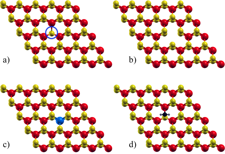
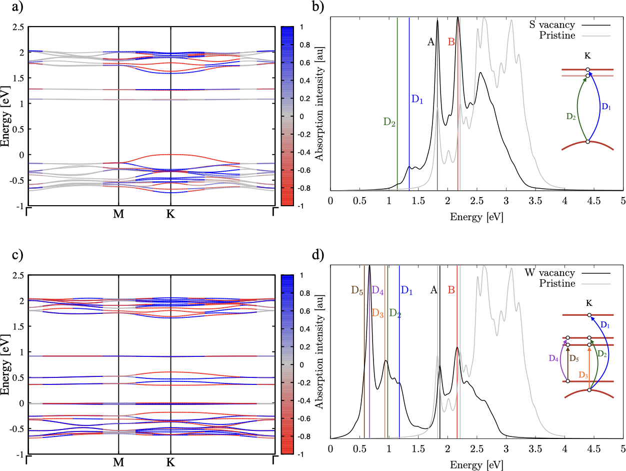
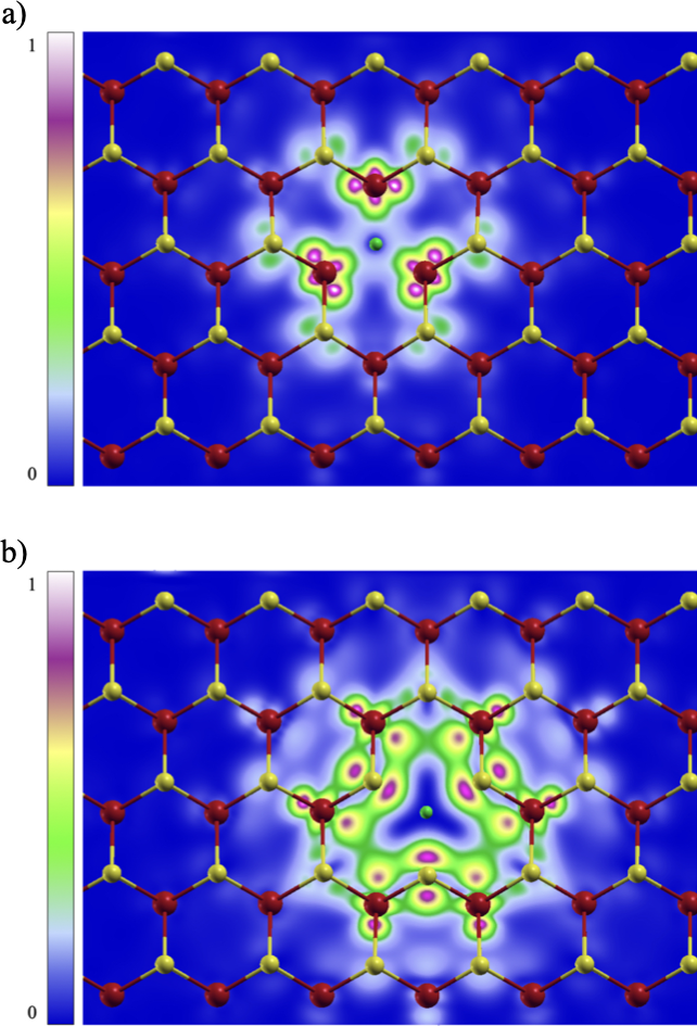
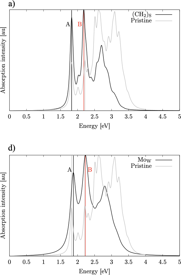
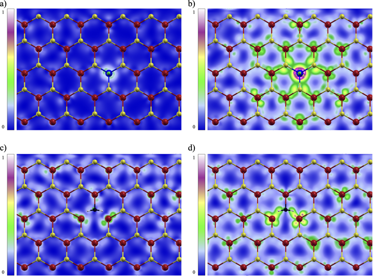
Table of Contents