Monolithic Thin-Film Chalcogenide-Silicon Tandem Solar Cells Enabled by a Diffusion Barrier
Abstract
Following the recent success of monolithically integrated Perovskite/Si tandem solar cells, great interest has been raised in searching for alternative wide bandgap top-cell materials with prospects of a fully earth-abundant, stable and efficient tandem solar cell. Thin film chalcogenides (TFCs) such as the Cu2ZnSnS4 (CZTS) could be suitable top-cell materials. However, TFCs have the disadvantage that generally at least one high temperature step ( 500 °C) is needed during the synthesis, which could contaminate the Si bottom cell. Here, we systematically investigate the monolithic integration of CZTS on a Si bottom solar cell. A thermally resilient double-sided Tunnel Oxide Passivated Contact (TOPCon) structure is used as bottom cell. A thin ( 25 nm) TiN layer between the top and bottom cells, doubles as diffusion barrier and recombination layer. We show that TiN successfully mitigates in-diffusion of CZTS elements into the c-Si bulk during the high temperature sulfurization process, and find no evidence of electrically active deep Si bulk defects in samples protected by just 10 nm TiN. Post-process minority carrier lifetime in Si exceeded 1.5 ms, i.e., a promising implied open-circuit voltage (i-Voc) of 715 mV after the high temperature sulfurization. Based on these results, we demonstrate a first proof-of-concept two-terminal CZTS/Si tandem device with an efficiency of 1.1% and a Voc of 900 mV. A general implication of this study is that the growth of complex semiconductors on Si using high temperature steps is technically feasible, and can potentially lead to efficient monolithically integrated two-terminal tandem solar cells.
keywords:
Tandem, Photovoltaic, Silicon, TOPCon, CZTS, Titanium NitrideMSC:
[2019] 00-01, 99-001 Introduction
The current global uptake of photovoltaic (PV)-based solar energy has been enabled by the remarkable developments in crystalline Silicon (c-Si) solar cell technologies, both in terms of module efficiencies and costs, with market shares consistently around 90% for decades – a figure which is expected to remain unchanged in the near future [1, 2, 3]. However, as the Si cell efficiency approaches the Shockley-Queisser (SQ) single-junction limit [4], further cell improvements are now only incremental, and the focus is instead on systems cost reduction and raw material utilization [2, 3].
Multi-junction solar cells can achieve higher efficiencies than the single-junction SQ limit, with AM 1.5 limits of around 45% and 50.5% for double (also called tandem) and triple-junction solar cells, respectively [5, 6]. However, to transition the global PV market from a single- to a multi-junction solar cell technology, the following conditions must be met: 1) The efficiency improvements should not sacrifice cost competitiveness, namely in terms of the Levelized Cost of Electricity (LCOE); 2) The raw materials used should be abundant, inexpensive and non-toxic; 3) Each individual junction, as well as the full device, must be stable and have a lifetime of decades [7, 8].
Various multi-junction cell configurations have been proposed and demonstrated experimentally, particularly with Si and III-V semiconductors, reaching efficiencies of 32.8% and 37.9% for tandem and triple-junction cells, respectively [9, 10, 11, 12]. In space applications, multi-junction III-V solar cells have been used almost exclusively since the late 1990s, but with costs not competitive with the single-junction c-Si technology for terrestrial applications [13, 14]. Out of all the possible multi-junction configurations, a monolithically integrated two-terminal (MI-2T) tandem device is considered a priori to be the most feasible for cost-competitive, large-scale applications, since it retains the module design simplicity of single-junction technologies and minimizes the total number of processing steps. Despite all of its potential advantages, MI-2T tandem devices are challenging to achieve in practice because every processing step has to be compatible and the properties of the preceding interface and layers should not be compromised [15].
c-Si is an excellent partner in a tandem solar cell for the same reasons that gave it a dominant position in the PV market. Its band gap of 1.12 eV is near ideal for a MI-2T tandem – when used together with an absorber with a bandgap of 1.72 eV, a theoretical maximum efficiency of close to 43% can be achieved [6, 9]. Recently, a lot of interest has been raised after a series of MI-2T Perovskite/Si tandem devices achieved efficiencies above 25%, with the current record set at 28% [16, 17, 18], a value higher than that of the best Si solar cell.
Thin film chalcogenides (TFCs) such as CdTe, CuInxGa1-x(SySe1-y)2 (CIGSSe), Cu2ZnSn(SxSe1-x)4 (CZTSSe) and their respective solid solutions and cationic substitutions could be suitable alternatives to Perovskites due to their increasing single-junction solar cell efficiencies, competitive production costs and superior stability. Indeed, a 16.8% Cd1-xZnxTe/Si tandem cell has been demonstrated using low temperature molecular beam epitaxy (MBE) [19]. However, in most cases, TFCs have the disadvantage that a high temperature step 500 °C ) is needed, contrary to Perovskites which can be processed at low temperatures ( 200 °C) [15, 16]. Recently, a promising monolithic Si/CGSe tandem cell with an efficiency of 10% has been reported [20], where the CGSe layer was produced by co-evaporation and high-temperature annealing. The authors report that the bottom Si cell J-V curve was not degraded during the top cell processing, however no further details were provided regarding the characterization of the bottom Si cell, and it is unclear what would be the resilience of the bottom cell for different processing parameters, or different deposition methods. Hence, to the best of our knowledge, the implications of high temperature processing on the feasibility of a MI-2T TFC/Si tandem device remain relatively unknown and have not yet been directly assessed experimentally.
In this work, we discuss the challenges of producing TFC/Si MI-2T tandem devices, using the sulfide kesterite Cu2ZnSnS4 (CZTS), an earth abundant and environmentally friendly representative of the TFC group. In particular, we assess the contamination and degradation of a Tunnel Oxide Passivated Contact (TOPCon) Si bottom cell during the CZTS processing steps. We test the introduction of a thin titanium nitride (TiN) diffusion barrier layer between the Si and CZTS structures and use the results to evaluate the process compatibility between CZTS and Si. We show that compatibility can be achieved, and report on a first proof of concept CZTS/Si tandem solar cell with an efficiency of 1.1% and a Voc of 900 mV, a value higher than that of each respective individual reference cell. Moreover, we suggest strategies for future device improvement.
1.1 The Top Cell: CZTS
The kesterite sulfide-selenide CZTSSe attracted interest as an all earth abundant alternative to CIGSSe consisting of non-toxic elements (in particular the sulfide CZTS), achieving solar cell efficiencies above 10% using industrially upscalable methods such as sputtering [21]. Sulfide CZTS, in particular, has some features which suggest that it could be a promising tandem partner for Si. Through different solid solutions and cationic substitutions, the bandgap of kesterites can be tuned – for instance, through Ge or Ag incorporation the bandgap of sulfide CZTS can be increased from the nominal 1.5 eV to about 2.1 eV, an ideal range for tandem applications [22, 23, 24, 25, 26, 27]. Moreover, CZTS and Si are closely lattice-matched, with an a-axis lattice mismatch of less than 0.1% [28, 29]. This means that heteroepitaxial growth of CZTS on Si could be possible, and this has indeed been proven experimentally [30, 31, 32]. While this allows in principle for growing CZTS/Si tandem devices epitaxially (free of grain boundaries), epitaxial growth of CZTS on Si with the necessary tunnel junction structures has not been demonstrated yet.
So far, the TFC solar cells with the highest efficiencies, in particular in the case of CZTS, involved at least one high temperature step [29] (with the notable exceptions of MBE [19] and monograin technology [33]). Herein, we argue that one of the biggest challenges towards a TFC/Si MI-2T tandem device could be a cross-contamination of the bottom Si cell with metallic elements such as Cu or chalcogens like S, during the high temperature step.
1.2 The Bottom Silicon Cell: Tunnel Oxide Passivating Contacts (TOPCon)
The tunnel oxide passivating contact (TOPCon) structure has played a key role in the recent silicon solar cell efficiency improvements [34, 35, 36, 37, 38]. The structure consists of stacks of thin ( 1.2 – 1.5 nm) SiO2 layers (tunnelling oxide, TO) and highly doped (Phosphorous or Boron) polycrystalline silicon layers (PolySi) on both sides of a crystalline silicon (c-Si) wafer. This structure provides excellent surface passivation and carrier selectivity. Consequently, high implied Voc of 750 mV and external Voc of up to 739 mV have been achieved [39]. In contrast to its aSi:H heterojunction counterpart, the TOPCon structure alone is resilient to high temperature annealing up to 900 °C, which is well above the typical annealing temperatures used in the synthesis of chalcogenide semiconductors and in other front and backend processes. Moreover, the simple one-dimensional current transport and full coverage of contacts at both sides allows for very low contact resistivity and thereby low fill-factor (FF) losses [40]. A major drawback of a front PolySi contact in a single-junction device is the parasitic absorption losses in the blue wavelength region within the PolySi layer. As a result, a short-circuit current density (Jsc) loss of 0.5 mA/cm2 is expected for every 10 nm of PolySi in a single junction cell [41]. However, this loss is not a limitation in a tandem configuration, where the high-energy photons are absorbed in the top cell. Thus, the double-sided TOPCon structure may be an ideal candidate for double-junction tandem solar cell.
1.3 The Need for a Diffusion Barrier Layer
When a nearly complete silicon solar cell is used as substrate for the growth of a TFC, there is a risk of contamination from metallic and chalcogen elements that should be thoroughly assessed. In this contribution, we study the case of co-sputtered CZTS precursors from Cu, ZnS and SnS targets on c-Si model substrates. During co-sputtering, the impinging energetic ions and neutrals can directly cause sputter damage, or contaminate the Si bulk by implantation. After co-sputtering, CZTS is formed by high temperature reactive annealing in a sulfur atmosphere. Here, the elements Cu, Zn, Sn and S (the latter both from the precursors and from the atmosphere) may diffuse into the Si bulk. We note that this high temperature step is of particular interest, since it is nearly ubiquitous in high-quality TFC fabrication, even in single-step processes (for instance co-evaporation of CIGS).
Copper contamination in silicon deserves special consideration as it is a common element of both the CIGS and the CZTS group of alloys and, most importantly, because it is one of the most common detrimental contaminants known in crystalline Si, as widely reported in the photovoltaic and integrated circuit industries [42, 43, 44]. Copper has a high diffusivity in Si, and can diffuse through the entire thickness of a Si wafer at room temperature in a matter of hours, although the solid solubility is 1015 cm-3 at the relevant temperatures [42]. Cu exhibits a complex defect physics in Si, leading to point defects and complexes, decoration of extended defects, precipitation of copper silicides, out-diffusion to the surface and segregation phenomena. In particular, copper silicides have been shown to lead to mid-gap defect traps in Si and a high recombination activity [45], detrimental in solar cells.
Although studied to a lesser extent than copper, the other elements of CZTS could also be harmful contaminants for a bottom Si cell. Zinc can introduce near-midgap defect levels in Si as shown in pure diffusion studies [46, 47, 48]. Tin was studied in particular as a dopant to improve the radiation resistance of c-Si devices, but was also found to form midgap states in Si [49, 50]. Finally, sulfur was studied notably in “black silicon” processing, where it was found that its incorporation creates deep bandgap states, which increase the infrared light absorption in Si, making it appear more “black” [46, 51, 52].
Here, we suggest that one possible way to prevent bottom cell contamination is using a diffusion barrier layer at the bottom-cell/top-cell interface. In general, a barrier layer must have properties such as mechanical stability, good adhesion, high temperature stability and low diffusivity for the contaminating elements. For tandem solar cell applications, it must also be electrically conductive and transparent in the near infrared region. To the best of our knowledge, only one published work directly addresses this problem, suggesting the use of ZnS as a barrier layer for the growth of CZTS/Si tandem cells [53]. In this work, we propose titanium nitride (TiN) as a barrier layer at the CZTS/Si interface, a novel concept for the monolithic integration of a top thin-film cell on a bottom Si cell. TiN has been extensively studied as a barrier layer for copper metallization in integrated circuits, although it is arguably not the most effective barrier known against Cu diffusion [44, 54, 55]. TiN has been employed as a back contact modification and barrier against over-sulfurization (or over-selenization) in single-junction CZTSSe cells, and proved to be compatible with up to 9% efficiency devices [56, 57, 58, 59, 60]. Due to its poor transparency, the TiN thickness must be limited to only a few nm.
By contrast, in a MI-2T Perovskite/Si tandem solar cell, a Si-based tunnel junction or a simple interface recombination layer based on a transparent conductive oxide (TCO) can be used to achieve high performing devices [15, 16]. This could also be a possibility if contamination-free growth of TFCs on Si can be proven. In this regard, it is noteworthy to mention that there are studies suggesting that some TCO substrates could be compatible with TFC growth conditions [24, 61].
2 Materials and Methods
A set of double side polished 100 mm diameter, 1 .cm, 350 m thick, (100) n-type Cz-Si wafers were used.
The fabrication process of the TOPCon structure is as follows. After the wafers were cleaned in RCA1 (H2O2:NH4OH:5H2O) and RCA2 (H2O2:HCl:5H2O) mixtures, 1.2 nm of SiO2 (tunnel oxide or TO) was grown by chemical oxidation in a 65 %wt HNO3 solution at 95 °C. Subsequently, 40 nm PolySi layers were deposited using Low Pressure Chemical Vapor Deposition (LPCVD) at 620°C, using SiH4, B2H6, or PH3 as precursors for p+ or n+ PolySi layers, respectively. The samples were then annealed in N2 at 850 °C for 20 min for further dopant diffusion and activation. All samples have a symmetrical passivation of TO/n+PolySi on both sides, except in two cases: for Deep Level Transient Spectroscopy (DLTS), this passivating stack was not used, and for the tandem solar cell fabrication, an asymmetrical passivation was used, with TO/n+PolySi on the front and TO/p+PolySi on the rear side. In the fabrication of tandem cells, a hydrogenation process was performed on the as-passivated bottom cell precursor wafer. For this purpose, a sacrificial 75 nm hydrogenated SiN (SiN:H) layer was deposited on both sides of the wafer using Plasma Enhanced Chemical Vapor Deposition (PECVD) at 300 °C. After a hydrogen drive-in process at 400 °C for 30 min in N2 atmosphere, the SiN:H layers were stripped in a buffered HF solution. The benefits of this SiN hydrogenation process are similar to those achieved by annealing in forming gas [62]. A few experiments used an alternative surface passivation with 40 nm Al2O3, deposited by Atomic Layer Deposition (ALD) using tetramethylammonia (TMA) and H2O as precursors.
TiN barrier layers ( 25 nm) were deposited in a Picosun Plasma-Enhanced ALD (PEALD) system using TiCl4 and NH3 precursors at 500 °C. To improve the optical transparency of TiN, the ALD chamber was not passivated for nitride depositions in the tandem cell fabrication. As a result, a slightly higher amount of oxygen is present in the TiN layer used in the tandem cell. Metallic 100 nm Cu layers were sputtered on the TOPCon structure and annealed at 550 °C in vacuum ( mbar). CZTS precursors were co-sputtered from Cu, ZnS, and SnS targets, and annealed in a graphite box with a reactive N2 atmosphere containing 50 mg of S pellets, at dwell temperatures of 525 – 575 °C for 30 min, in order to form CZTS films with a thickness around 300 nm. This CZTS thickness was chosen based on optical simulations (not shown here) and photocurrent density (Jsc) results from single junction CZTS devices, in order to match the photocurrents of the two cells. Prior to lifetime, Secondary Ion Mass Spectrometry (SIMS), and DLTS measurements, the Cu, CZTS and TiN layers were removed (after the sulfurization/annealing step) in a mixture of H2O2:4H2SO4 (piranha) and RCA1 solutions, followed by a dilute HF dip. For the Rutherford Backscattering Spectroscopy (RBS) measurements, only piranha was used.
The effective minority carrier lifetime (eff) of Si was measured by the microwave detected photoconductance decay method (-PCD) in steady-state configuration at 1-sun illumination using an MDP lifetime scanner from Freiberg Instruments. The reported lifetime values were obtained from maps of the whole wafer area with 1 cm edge-exclusion margin. The i-Voc values were calculated based on the method described in [63].
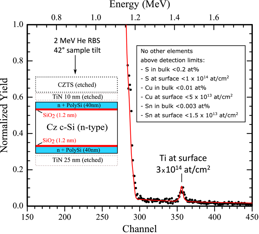
The in-diffusion depth profile were measured by SIMS and RBS on selected samples. The SIMS depth profiles were obtained from a Cameca IMS-7f microprobe. A 10 keV O2+ primary beam was mainly utilized, and rastered over m2, and the positive ions were collected from a circular area with a diameter of 33 m. For sulfur, however, a 5 keV Cs+ primary beam was employed, and clusters of 32S133Cs were detected to minimize matrix effect and avoid mass interference. The quantification of Cu depth profiles was obtained by measuring an implanted reference sample, ensuring a 10 % error in accuracy. The crater depths were measured by a Dektak 8 stylus profilometer, and a constant sputter erosion rate was assumed for the depth calculation. The RBS measurements were done using 2 MeV He ions and a silicon PIN diode detector under a 168∘ angle. The collected RBS data were analyzed and fitted using RUMP [64].
DLTS was used to characterize electrically active defects in the Si bulk. DLTS measurements were performed on circular Schottky diodes (1 mm diameter), where 50 nm thick Pd contacts were deposited by thermal evaporation. The backsides were coated with silver paste to form an ohmic contact. During the measurements the diodes were held at V reverse bias and pulsed to 1 V, filling all majority traps within the depletion width of 1 m. The samples were cooled to 35 K by a closed-cycle cryostat and six rate windows (with lengths 2i 10 ms, = 1, , 6), were used to record the capacitance transients while heating to 300 K. The transients were multiplied by a lock-in weighting function for improved signal extraction. Further details on the method and setup are given in [65].
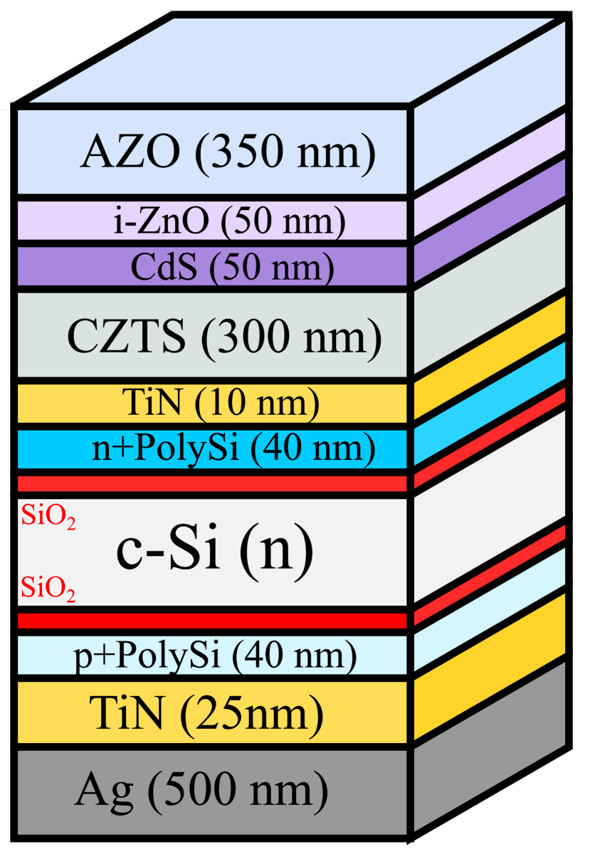
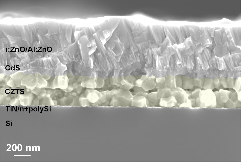
For the monolithic CZTS-Si tandem device, a 50 nm CdS layer, by chemical bath deposition, was used as the buffer to form the p-n heterojunction of the top cell, followed by a 50 nm intrinsic i-ZnO and a 350 nm Al-doped ZnO (AZO) as the TCO layer. Both window layers, i-ZnO and AZO, were deposited using reactive sputtering. A 500 nm Ag layer was thermally evaporated as the back contact. No front metal contacts were used for simplicity, as the active tandem cell areas were only 33 mm2. The full tandem solar cell was post-annealed on a hot plate in air at 250 °C for 15 min, in order to improve the properties of the CZTS/CdS heterojunction (see Figure S13).
The J-V characteristic curves of the solar cells were measured at near Standard Test Conditions (STC: 1000 W/m2, AM 1.5 and 25 °C). A Newport class ABA steady state solar simulator was used. The irradiance was measured with a cm2 Mono-Si reference cell from ReRa certified at STC by the Nijmegen PV measurement facility. The temperature was kept at 25 3 °C as measured by a temperature probe on the contact plate. The acquisition was done with 2 ms between points, using a 4 wire measurement probe, from reverse to forward voltage. The external quantum efficiency (EQE) of the tandem cell was measured using a QEXL setup (PV Measurements) equipped with a grating monochromator, adjustable bias voltage, and a bias spectrum.
Room temperature photoluminescence (PL) measurements were done on complete cells with an excitation wavelength of 785 nm using a modified Renishaw Raman spectrometer equipped with a Si CCD detector, in confocal mode.
Scanning electron microscopy (SEM) images of the tandem cell structures were acquired using a Zeiss Merlin field emission electron microscope under a 5 kV acceleration voltage.
3 Results and Discussion
3.1 Minority Carrier Lifetime Measurements on Si
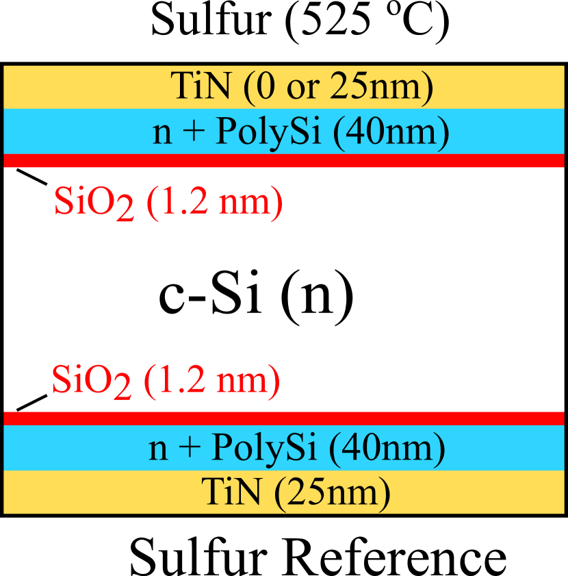
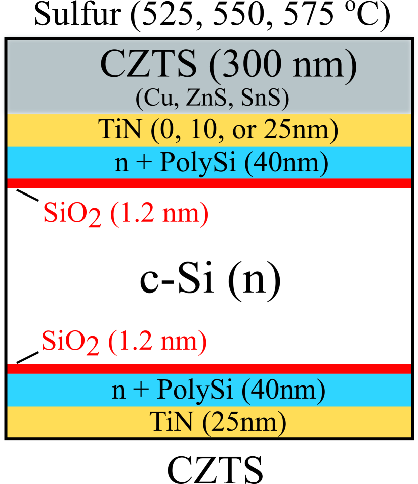
The minority carrier lifetime of Si is used as a figure of merit throughout the paper to evaluate the bottom cell after CZTS and tandem cell processing. For this purpose, 10 symmetrically passivated wafers with an as-passivated mean lifetime of 2.65 0.52 ms were prepared. The uniform surface passivation quality across the wafer set ensures that the passivation and wafer qualities are not variables in the subsequent studies. More details on the passivation statistics are shown in the supplementary information (Figure S1). Three different set of samples were prepared, as listed in Table 1 and illustrated in Figure 1. All the samples have a 25 nm TiN layer on the backside, to eliminate any unwanted contamination from that side during the different processing steps.
| Sample | TiN Thickness (nm) | Annealing atm./T °C | Purpose |
|---|---|---|---|
| Cu Reference | 25 | Vacuum/550 | Compare metallic Cu to CZTS |
| Sulfur Reference | 0, 10 | Sulfur/525 | Isolate the effect of S |
| CZTS | 0, 10, 25 | Sulfur/525, 550, 575 | Integration of CZTS on Si |
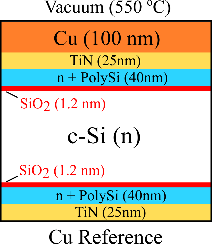
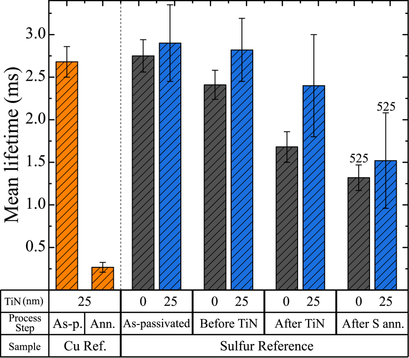
In Figure 2, the Si minority carrier lifetime of the Cu Reference sample is shown as a function of the annealing time. In this case, the TiN barrier layer fails after a 15 min annealing at 550 °C , with a 73% loss of lifetime. The lifetime is further degraded with increasing annealing time. These results indicate that, for this temperature range, the 25 nm TiN barrier layer provided insufficient protection of the sample against Cu diffusion.

In Figure 3 (a) and (b), the Si carrier lifetime results for the Sulfur Reference and CZTS cases are shown. Here, the lifetime was monitored after each major processing step, namely the TiN deposition and the CZTS annealing steps. From the As-Passivated to the Before TiN step, there was a waiting time on the order of a few weeks, causing a slight decrease in the lifetime due to aging. The final lifetimes of Figure 3 (a) are reduced to 45-50% of the As-passivated value after annealing in a sulfur atmosphere, suggesting the role of S as a contaminating species. The 60 min point of the Cu Reference carrier lifetime of Figure 2 is included in Figure 3 (a) for comparison, showing that the impact of the S atmosphere is less severe than that of metallic Cu. Further details and lifetime maps of the Cu Reference and Sulfur Reference carrier lifetime measurements are shown in the supplementary Figure S2 and Figure S3, respectively.
In Figure 3 (b), the key observation is that the final lifetime values after CZTS processing are significantly higher than that of the Cu Reference case, in spite of the fact that metallic Cu is present in the co-sputtered CZTS precursors. One possible explanation for this milder contamination effect is that the driving force for the formation of Cu2-xS phases (the binary phases in the CZTS phase diagram with the lowest melting point [29]) competes directly with the diffusion of the available Cu into Si. Therefore, the competing Cu2-xS formation reaction reduces the driving force for Cu diffusion into Si. Moreover, the lifetime values after CZTS processing are comparable to the Sulfur Reference case, indicating that having CZTS in addition to a sulfur atmosphere does not lead to additional lifetime deterioration.
The influence of the annealing temperature was also studied in the CZTS case with a series of different annealing temperatures at 525 °C, 550 °C and 575 °C, for the cases without TiN and 10 nm TiN, as shown in the “After CZTS” step of Figure 3 (b). One single measurement with a TiN thickness of 25 nm is included as reference for comparison in the subsequent studies. However, this thickness would be too high for use in a tandem cell (due to poor transparency). The annealing series shows that while the 10 nm TiN case seems to follow a trend with increasing temperature, this is not true for the case without TiN. This is likely due to spatial variations in the sample’s lifetime, shown by the uncertainty bars, which have a magnitude comparable to the variations seen in the temperature series. Moreover, it can be seen that the 0 nm and 10 nm TiN series have comparable absolute carrier lifetimes after CZTS processing. To further understand this behavior, we plot in Figure 4 the same results but scaled to the respective “After TiN” lifetimes. By doing this, it becomes clear that the lifetime deterioration during CZTS processing is more significant when no TiN is present. This scaling procedure is also justified as it can be noted in both Figure 3 (a) and (b) that the final (post-process) lifetime values are affected by a significant and non-uniform loss in lifetime during the TiN deposition step. The reason for this loss may be attributed to a minor contamination originating from the ALD chamber and stainless steel carrier used during the deposition (e.g. iron contamination). We discuss this issue in greater detail and show additional experimental data in the SI (see Figure S8). However, further future investigation will be required to fully clarify this effect.
Despite the degradation throughout the processing, the final lifetimes are above 1 ms, which corresponds to an i-Voc above 700 mV. This encouraging result indicates that the performance of the bottom silicon cell may not necessarily be compromised as a result of the CZTS synthesis. However, given the comparable absolute lifetime values, regardless of the TiN thickness, it is not yet clear from the lifetime results alone whether the use of a TiN barrier layer would be useful.
To further evaluate whether the observed degradation is related to a bulk contamination or TO/n+PolySi surface depassivation, a complementary experiment was conducted where a silicon wafer was passivated only at the end of the CZTS processing, after etching the CZTS and TiN layers. Any possible unforeseen effects caused by the TO/n+PolySi passivation are avoided by using this configuration. We refer to this as the “end-passivated” sample. Here, we repeated the Si/TiN(25nm)/CZTS sample, except using a non-passivated bare silicon wafer (no TO/n+PolySi passivation) as the substrate. Subsequent to the CZTS and TiN etching and cleaning, 40 nm ALD Al2O3 was deposited on both sides for surface passivation. The results, plotted in Figure 5, indicate a tolerable 14 mV decrease in i-Voc ( 30% lifetime decrease) for the sample with CZTS processing compared to the clean reference sample.
Even though this experiment does not directly clarify the effect of the PolySi layer on the diffusion of contaminants from CZTS processing, it shows that relatively high-end lifetimes can be achieved without using a PolySi layer. This suggests that there is some flexibility of design in the bottom Si cell, and offers new perspectives for future tandem integration experiments.

3.2 SIMS and RBS Analysis
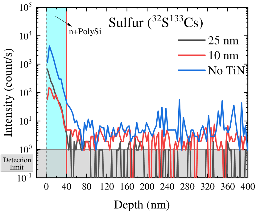
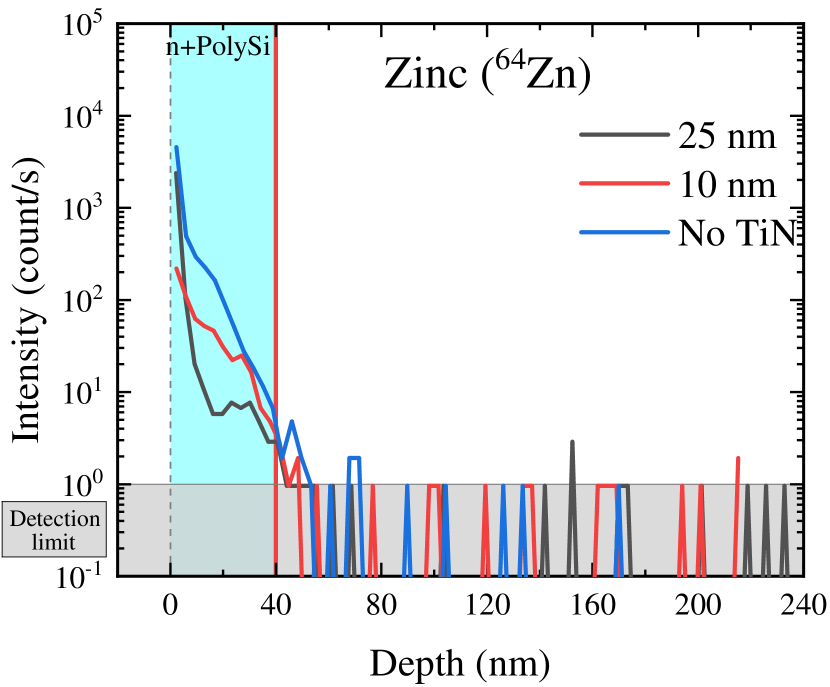
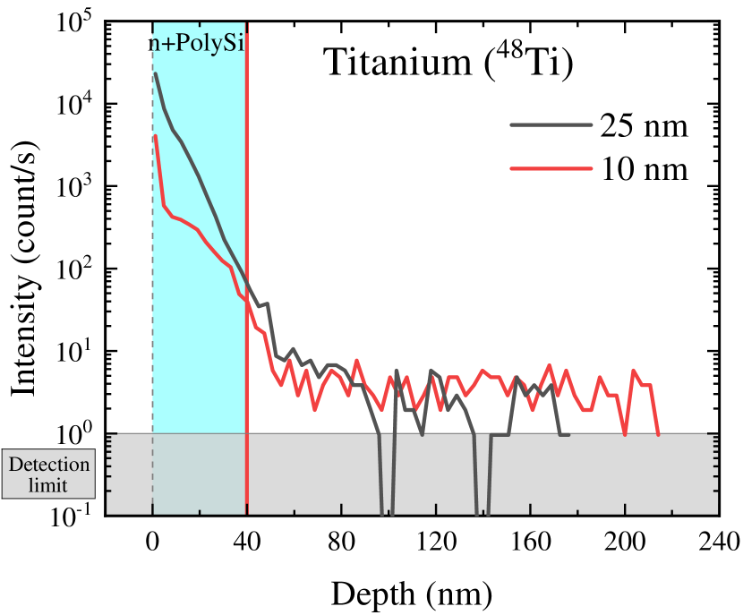
To correlate the lifetime results with possible diffusion of contaminants into the Si bulk, SIMS and RBS measurements were performed on selected Cu Reference and CZTS-processed samples (after selective removal of the Cu, TiN and CZTS layers). The SIMS results are illustrated in Figure 6. For the Cu Reference samples, the corresponding quantitative Cu SIMS depth profiles are shown in Figure 6 (a). A clear diffusion tail into the c-Si bulk is detected in all cases, with a Cu peak concentration of up to 1020 cm-3 occurring in the PolySi. Furthermore, an increase in Cu concentration is seen with increasing annealing time, which is in qualitative agreement with the lifetime results of Figure 2. In Figure 6 (b), a quantitative Cu profile is presented for the CZTS-processed samples annealed at 525 °C. The Cu profiles reveal that for the No TiN and 10 nm TiN samples, there is a diffusion tail extending at least 100 nm into the Si bulk, but for the 25 nm TiN case the Cu concentration drops sharply to below detection limits after the PolySi. In all three cases, the Cu concentration is 2 – 3 orders of magnitude lower compared to the Cu Reference case, which helps to justify their significantly higher lifetimes. Into the Si bulk (close to the surface), the Cu concentration is always lower than 1018 cm-3, which in Si corresponds to 0.002 at% (or 20 ppm).
Depth profiles of other relevant elements during CZTS processing, namely Zn, Sn, S and Ti (from TiN) are shown in Figure 6 (c) to (f). Other elements than Cu appear to be at background levels or near detection limits into the c-Si bulk.
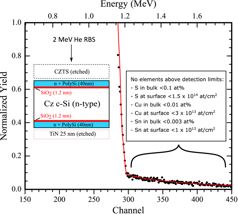
To complement the SIMS analysis, RBS measurements were done on the CZTS-processed samples with 0 nm and 10 nm TiN, annealed at 525 °C. The results are illustrated in Figure 7 (a) and (b), respectively. Since all the potential contaminant elements are heavier than Si, the RBS data is zoomed in at energies higher than the Si onset. None of the possible contaminants are detected in Si, except for some Ti at the surface, which was not fully removed during the piranha etching (confirmed with SEM, not shown here). This means that an estimate for the upper limit for the concentration of these contaminants can be established, given by the sensitivity of the measurement itself. For the measurement conditions of Figure 7 (a) and (b), these upper limits are given in the figure insets. In the particular case of Cu, which was also quantitatively measured by SIMS, RBS shows that its concentration has to be below 0.01 at%, agreeing with the value of below 0.002 at% obtained by SIMS.
3.3 DLTS Analysis
To further assess the influence of these possible contaminants, DLTS measurements were made on CZTS-processed samples annealed at 525 °C. Here, samples without the TO/n+PolySi passivation were prepared as no Schottky contact (required in our DLTS setup) could be obtained between the metal electrode and the heavily-doped PolySi. An unprocessed bare “Reference” wafer was also included to rule out any possible pre-existing defects. The results are plotted in Figure 8. It is shown that the samples with 10 nm TiN, 25 nm TiN and the Reference wafer do not have any DLTS signal, but the No TiN sample exhibits peaks related to electrically active defects, with two features peaking at 175 K and 275 K. The 175 K peak shows a broadening towards the lower temperature side, which may be related to several overlapping defect signatures or extended defects [66]. In the case of extended defects, an exponential decay in emission rate may not hold, and will influence the extracted activation energies and apparent capture cross-sections from an Arrhenius plot of the corresponding DLTS peak [67]. This peak near 175 K might come from several defects associated with precipitates of Cu [34, 68], but further measurements would be required to assign this unambiguosly. The peak at 275 K could be used instead for making an Arrhenius plot. This peak has a broad shape due to its very low capture cross-section of cm2, and its energy level was found to be 0.16 eV below the conduction band edge, as extracted from the Arrhenius plot. The level at eV has previously been reported in Cu diffused Si and shown to originate from interstitial copper or a complex of interstitial copper by Istratov et al [69]. More details on the DLTS results, analysis and Arrhenius plot can be found in the supplementary information (Figure S4 and Figure S5).
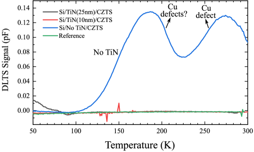
Based on these findings, 10 nm of TiN seems to be sufficient to prevent the formation of electrically active defects in the Si bulk. This thickness was thus selected to prepare a full CZTS/Si tandem solar cell.
3.4 Fabrication of a Monolithic CZTS/Si Solar Cell
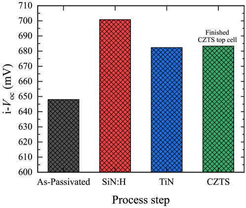
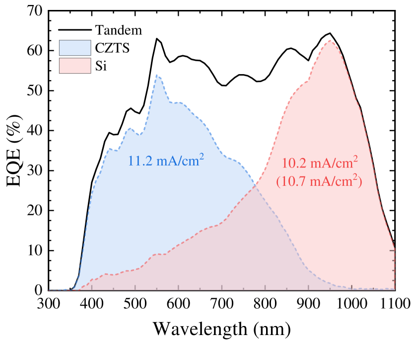
The effective minority carrier lifetime of the silicon bottom cell was monitored at different steps of the fabrication process, similar to Section 3.1. However, the samples are now asymmetrically passivated (with TO/p+PolySi on the backside). An additional SiN hydrogenation step (to improve the passivation quality) was also included. The corresponding i-Voc is shown in Figure 9 as a function of process steps. Figure 9 shows that the i-Voc of the silicon bottom cell was slightly degraded after the TiN deposition step. As mentioned in Section 3.1, we suggest that this degradation may be due to iron contamination (originating from the ALD chamber). However, given the additional hydrogenation step of the p-PolySi explained above, a partial loss in the hydrogen passivation could occur in this case (see supplementary Figure S8). The i-Voc, however, does not degrade further during the full fabrication of the CZTS top cell. This demonstrates that 10 nm TiN was an effective diffusion barrier. The J-V curves, EQE and schematic illustration of the tandem device are shown in Figure 10 (a), (b) and (c), respectively.
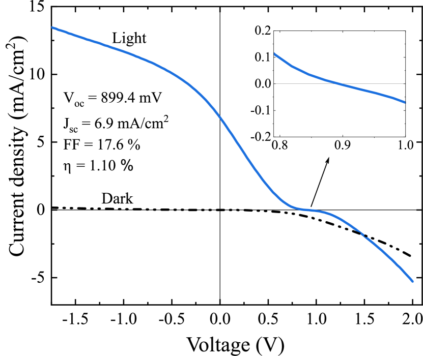
As seen in Figure 10 (a), the tandem cell shows a Voc of 900 mV, which is higher than that expected for each individual junction separately, under the same conditions (see supplementary Figure S6). The efficiency, however, is low (1.10%) and the light J-V curve shows a clear “rollover” effect, which is characterized by a distortion of the J-V curve, causing a very low fill-factor (FF). The magnitude of the Jsc seems to be also affected by the distortion as the EQE measurement in Figure 10 (b) shows a Jsc of around 11 mA/cm2 for each individual cell. We attribute the low efficiency to a combination of the rollover effect and a poorer CZTS top cell compared to the single junction CZTS cell, as will be elaborated below.
This rollover effect, with S-shaped J-V curves, has been reported previously for non-optimal tandem cells, associated with the reverse breakdown voltage regime of the top cell when the tandem is current-mismatched [70]. While this explanation is certainly plausible here, we note that other effects may cause a rollover effect in single-junction solar cells, as was reviewed recently in [71]. This occurs when there is one or more barriers to current extraction throughout the solar cell under illumination. This barrier can be due to the presence of Schottky barriers in non-ohmic contacts (namely the n+PolySi/TiN or TiN/CZTS interfaces), or a non-ideal p-n junction, leading to a voltage-dependent current blocking behavior. In particular, this effect has been reported for non-ideal p-n junctions in single-junction CZTS cells [72], and we have also seen it in our internal experiments for CZTS/CdS p-n junctions when the synthesis parameters were not ideal (see supplementary Figure S9). For the tandem cell, our TiN barrier layer was produced in an unpassivated ALD chamber, which improves the optical transparency of TiN by incorporating some oxygen, leading to a TiOxNy film. However, an excessive amount of oxygen can be detrimental, as it is known to increase the sheet resistance of TiN [73]. It has been reported that the presence of 10-15 % oxygen in TiN leads to formation of a Schottky diode with a barrier height of 0.55 eV on n-type Si (100) [74]. In the case of a single Si cell, we found evidence that using a similar 10 nm TiOxNy layer in-between the n+PolySi and TCO layers can cause a roll-over behavior on single junction Si cells (see supplementary Figure S10). Thus, the results of this work suggest that the ideal compromise between transparency and electrical properties in the TiN layer might not have been reached in this initial device, and this will be investigated in future work by tuning the TiOxNy composition. Furthermore, a rollover effect has been reported in CIGS at the Mo/CIGS interface on non-glass substrates, where there is no natural inclusion of Na (or other alkali elements) in the absorber layer. It was shown that this effect can be completely eliminated by providing a sufficient amount of Na [75]. This is particularly relevant in this work, as the growth of CZTS is also substrate dependent, and no intentional Na was added in the fabrication of the tandem cell.
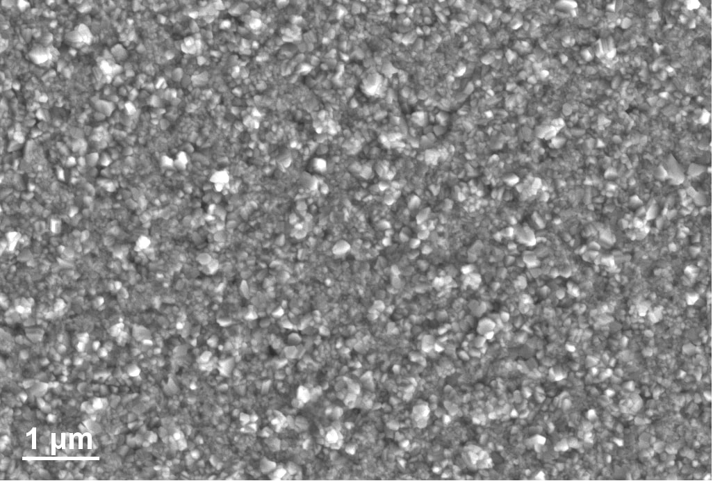
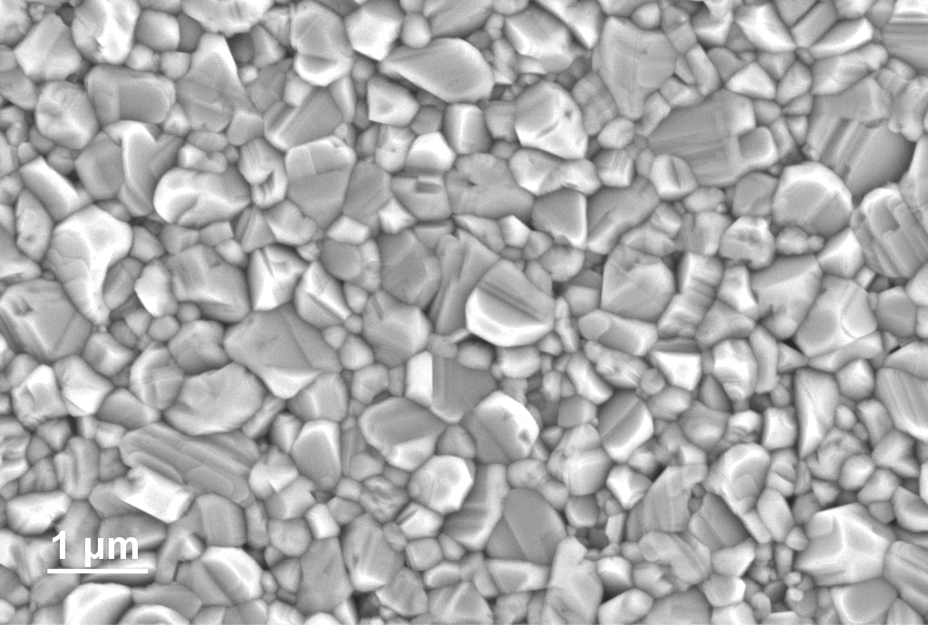
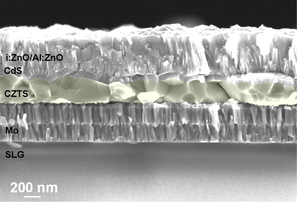
To explore these issues, we compare the results of our tandem device to a baseline single-junction CZTS cell where the CZTS thickness was reduced from the typical 1 m to a value of around 275 nm, similar to the value used for the tandem. This “thin CZTS cell” achieved an efficiency of 5.8%, with a Jsc of 15.8 mA/cm2 and a Voc of 585 mV (the J-V curve is shown in the supplementary Figure S11), which is fairly comparable to state of the art thin CZTS devices (with a record of 8.57% for a 400 nm thick CZTS [76]). However, when compared to the CZTS growth for the tandem cell, significant morphological differences between the two CZTS layers are noticeable. The morphology comparison is presented in Figure 11. The SEM top views of CZTS grown on the Si cell and on Mo/SLG, shown in Figure 11 (a) and (b), respectively, reveal a clear difference in grain size. The SEM cross-section of the tandem cell, in Figure 11 (c), shows that the CZTS exhibits a double layer structure, with a smaller grain size. In comparison, the CZTS grown with the same conditions on Mo-coated soda lime glass (SLG), shown in Figure 11 (d), has a single layer and larger grains. This indicates that the local conditions for CZTS growth are different in the two cases. In addition, CZTS photoluminescence (PL) measurements made on both the fully finished tandem and the thin CZTS cell, confirm that the thin CZTS cell has a significantly higher PL intensity (see supplementary Figure S12). We suggest that one possible reason for these differences is likely to be the contribution of Na diffusion from the glass, which is not available in Si. This possibility will be explored in future work.
The results of this work show that there is a margin for monolithically integrating a CZTS top cell on a full Si bottom cell using high temperature processing above 500 °C, without compromising the bottom cell. Given the constituting contaminant elements of CZTS (in particular Cu and S), we suggest that this study could be generalized to other thin film chalcogenide materials (many of which do contain Cu), and thereby open up the possibility of exploring new emerging wide band gap semiconductors as top cell alternatives.
4 Conclusion
We have assessed the potential of monolithically-integrated two-terminal tandem cells based on thin-film chalcogenides on Si, using CZTS and double-sided TOPCon Si as model system. We have investigated the use of a thin TiN barrier layer to protect the bottom Si cell from in-diffusion of metals and sulfur during the CZTS growth, and serve as interface recombination layer between the top and bottom cells at the same time. It was revealed that Cu contamination induced by CZTS growth on the Si bulk is significantly smaller than that from annealing of metallic Cu on Si. While traces of all CZTS elements (except for Sn) can be detected at the surface of c-Si after CZTS annealing, it was shown that the main contributor to the lifetime reduction in the bottom Si cell is Cu. Furthermore, it was shown that a TiN barrier layer as thin as 10 nm can effectively suppress the formation of Cu-related deep defects in Si. Based on these results, we presented a proof-of-concept monolithically integrated CZTS/Si tandem solar cell with an efficiency of 1.1% and a Voc of 900 mV, which shows an additive Voc effect. The i-Voc of the silicon bottom cell was retained during the full fabrication of the CZTS cell when a 10 nm TiN barrier was used. It is suggested that the poor performance of the tandem cell is mainly due to limitations in the CZTS top cell, namely difficulty of reproducing high-quality CZTS absorbers on non-glass substrates, where Na is not available. The possibility of non-ohmic blocking behavior at the TiN interfaces is also mentioned.
By showing that a full TOPCon Si solar cell can be processed at temperatures well above 500 °C in the presence of several critical contaminant elements – notably copper – without suffering from a severe degradation in lifetime and without forming deep defect levels, this work opens up the possibility of exploring other less known and future high bandgap compounds processed at high temperatures. This could allow for achieving high efficiency monolithically integrated tandem solar cells in the future.
5 Acknowledgements
A. Hajijafarassar (A.H.) and F. Martinho (F.M.) contributed equally to this work. This work was supported by a grant from the Innovation Fund Denmark (grant number 6154-00008A). F.M. would like to thank A. A. S. Lancia for the support on the J-V measurements.
6 Data Availability
All the data is available from the corresponding authors upon reasonable request.
References
References
- [1] M. Woodhouse, R. Jones-Albertus, D. Feldman, R. Fu, K. Horowitz, D. Chung, D. Jordan, S. Kurtz, On the Path to SunShot - The Role of Advancements in Solar Photovoltaic Efficiency, Reliability, and Costs doi:10.2172/1344202.
- [2] VDMA, International Technology Roadmap for Photovoltaic (ITRPV): Results 2017 Including maturity report 2018 (2018).
- [3] Markus Fischer, ITRPV 10th Edition 2019 - Report Release and Key Findings (2019).
- [4] W. Shockley, H. J. Queisser, Detailed Balance Limit of Efficiency of p‐n Junction Solar Cells, Journal of Applied Physics 32 (3) (1961) 510–519. doi:10.1063/1.1736034.
- [5] M. A. Green, Solar cells: Operating principles, technology and system applications, Prentice-Hall Inc., 1982.
- [6] M. A. Green, Silicon Wafer-based Tandem Cells: The Ultimate Photovoltaic Solution?, Vol. 8981, International Society for Optics and Photonics, 2014, p. 89810L. doi:10.1117/12.2044175.
- [7] Z. J. Yu, J. V. Carpenter, Z. C. Holman, Techno-economic viability of silicon-based tandem photovoltaic modules in the United States, Nature Energy 3 (9) (2018) 747–753. doi:10.1038/s41560-018-0201-5.
- [8] D. Bae, G. M. Faasse, G. Kanellos, W. A. Smith, Unravelling the practical solar charging performance limits of redox flow batteries based on a single photon device system, Sustainable Energy & Fuels 3 (9) (2019) 2399–2408. doi:10.1039/C9SE00333A.
- [9] Z. J. Yu, M. Leilaeioun, Z. Holman, Selecting Tandem Partners for Silicon Solar Cells, Nature Energy 1 (2016) 16137. doi:10.1038/nenergy.2016.137.
- [10] S. Essig, C. Allebé, T. Remo, J. F. Geisz, M. A. Steiner, K. Horowitz, L. Barraud, J. S. Ward, M. Schnabel, A. Descoeudres, D. L. Young, M. Woodhouse, M. Despeisse, C. Ballif, A. Tamboli, Raising the One-Sun Conversion Efficiency of III–V/Si Solar Cells to 32.8% for Two Junctions and 35.9% for Three Junctions, Nature Energy 2 (9) (2017) 17144. doi:10.1038/nenergy.2017.144.
- [11] M. A. Green, Y. Hishikawa, E. D. Dunlop, D. H. Levi, J. Hohl-Ebinger, M. Yoshita, A. W. Ho-Baillie, Solar Cell Efficiency Tables (Version 53), Progress in Photovoltaics: Research and Applications 27 (1) (2019) 3–12. doi:10.1002/pip.3102.
- [12] Sharp Corporation, Sharp Develops Solar Cell with World’s Highest Conversion Efficiency of 37.9% (2013).
- [13] P. Iles, Evolution of Space Solar Cells, Solar Energy Materials and Solar Cells 68 (1) (2001) 1 – 13, solar Cells in Space. doi:10.1016/S0927-0248(00)00341-X.
- [14] M. Yamaguchi, T. Takamoto, K. Araki, M. Imaizumi, N. Kojima, Y. Ohshita, Present and Future of High Efficiency Multi-Junction Solar Cells, in: CLEO: 2011 - Laser Science to Photonic Applications, 2011, pp. 1–3. doi:10.1364/CLEO_SI.2011.CMT5.
- [15] T. Todorov, O. Gunawan, S. Guha, A Road Towards 25% Efficiency and Beyond: Perovskite Tandem Solar Cells, Molecular Systems Design & Engineering 1 (2016) 370–376. doi:10.1039/C6ME00041J.
- [16] F. Sahli, J. Werner, B. A. Kamino, M. Bräuninger, R. Monnard, B. Paviet-Salomon, L. Barraud, L. Ding, J. J. Diaz Leon, D. Sacchetto, G. Cattaneo, M. Despeisse, M. Boccard, S. Nicolay, Q. Jeangros, B. Niesen, C. Ballif, Fully Textured Monolithic Perovskite/Silicon Tandem Solar Cells with 25.2% Power Conversion Efficiency, Nature Materials 17 (9) (2018) 820–826. doi:10.1038/s41563-018-0115-4.
-
[17]
Oxford
PV Perovskite Solar Cell Achieves 28% Efficiency, [Online: accessed
6-August-2019] (2018).
URL https://www.oxfordpv.com/news/oxford-pv-perovskite-solar-cell-achieves-28-efficiency -
[18]
PV Research Cell Record
Efficiency Chart, [Online: accessed 6-August-2019] (2019).
URL https://www.nrel.gov/pv/cell-efficiency.html - [19] J. W. Garland, T. Biegala, M. Carmody, C. Gilmore, S. Sivananthan, Next-Generation Multijunction Solar Cells: The Promise of II-VI Materials, Journal of Applied Physics 109 (10) (2011) 102423. doi:10.1063/1.3582902.
- [20] A. R. Jeong, S. B. Choi, W. M. Kim, J.-K. Park, J. Choi, I. Kim, J.-h. Jeong, Electrical Analysis of c-Si/CGSe Monolithic Tandem Solar Cells by Using a Cell-selective Light Absorption Scheme, Scientific Reports 7 (1) (2017) 15723. doi:10.1038/s41598-017-15998-y.
- [21] C. Yan, J. Huang, K. Sun, S. Johnston, Y. Zhang, H. Sun, A. Pu, M. He, F. Liu, K. Eder, L. Yang, J. M. Cairney, N. J. Ekins-Daukes, Z. Hameiri, J. A. Stride, S. Chen, M. A. Green, X. Hao, Cu2ZnSn(S,Se)4 Solar Cells with Over 10% Power Conversion Efficiency Enabled by Heterojunction Heat Treatment, Nature Energy 3 (9) (2018) 764–772. doi:10.1038/s41560-018-0206-0.
- [22] S. Oueslati, M. Grossberg, M. Kauk-Kuusik, V. Mikli, K. Ernits, D. Meissner, J. Krustok, Effect of Germanium Incorporation on the Properties of Kesterite Cu2ZnSn(S,Se)4 Monograins, Thin Solid Films 669 (2019) 315 – 320. doi:10.1016/j.tsf.2018.11.020.
- [23] E. Garcia-Llamas, J. Merino, R. Serna, X. Fontané, I. Victorov, A. Pérez-Rodríguez, M. León, I. Bodnar, V. Izquierdo-Roca, R. Caballero, Wide Band-Gap Tuning Cu2ZnSn1-xGexS4 Single Crystals: Optical and Vibrational Properties, Solar Energy Materials and Solar Cells 158 (2016) 147 – 153, Nanotechnology for Next Generation High Efficiency Photovoltaics: NEXTGEN NANOPV Spring International School & Workshop. doi:10.1016/j.solmat.2015.12.021.
- [24] M. Umehara, S. Tajima, Y. Takeda, T. Motohiro, Wide Bandgap Cu2ZnSn1-xGexS4 Fabricated on Transparent Conductive Oxide-Coated Substrates for Top-Cells of Multi-Junction Solar Cells, Journal of Alloys and Compounds 689 (2016) 713 – 717. doi:10.1016/j.jallcom.2016.08.039.
- [25] W. Gong, T. Tabata, K. Takei, M. Morihama, T. Maeda, T. Wada, Crystallographic and Optical Properties of (Cu,Ag)2ZnSnS4 and (Cu,Ag)2ZnSnSe4 Solid Solutions, Physica Status Solidi C 12 (6) (2015) 700–703. doi:10.1002/pssc.201400343.
- [26] G. Sai Gautam, T. P. Senftle, E. A. Carter, Understanding the Effects of Cd and Ag Doping in Cu2ZnSn(S,Se)4 Solar Cells, Chemistry of Materials 30 (14) (2018) 4543–4555. doi:10.1021/acs.chemmater.8b00677.
- [27] H. Cui, X. Liu, F. Liu, X. Hao, N. Song, C. Yan, Boosting Cu2ZnSn(S,Se)4 Solar Cells Efficiency by a Thin Ag Intermediate Layer Between Absorber and Back Contact, Applied Physics Letters 104 (4) (2014) 041115. doi:10.1063/1.4863951.
- [28] S. Adachi, Earth‐Abundant Materials for Solar Cells, John Wiley & Sons, Ltd, 2015, Ch. 2, pp. 21–66. doi:10.1002/9781119052814.ch2.
- [29] S. Schorr, Crystallographic Aspects of Cu2ZnSn(S,Se)4 (CZTS), John Wiley & Sons, Ltd, 2015, Ch. 3, pp. 53–74. doi:10.1002/9781118437865.ch3.
- [30] K. Oishi, G. Saito, K. Ebina, M. Nagahashi, K. Jimbo, W. S. Maw, H. Katagiri, M. Yamazaki, H. Araki, A. Takeuchi, Growth of Cu2ZnSn(S,Se)4 Thin Films on Si (100) Substrates by Multisource Evaporation, Thin Solid Films 517 (4) (2008) 1449 – 1452, proceedings of 2nd International Symposium on the Manipulation of Advanced Smart Materials. doi:10.1016/j.tsf.2008.09.056.
- [31] B. Shin, Y. Zhu, T. Gershon, N. A. Bojarczuk, S. Guha, Epitaxial Growth of Kesterite Cu2ZnSn(S,Se)4 on a Si(001) Substrate by Thermal Co-evaporation, Thin Solid Films 556 (2014) 9 – 12. doi:10.1016/j.tsf.2013.12.046.
- [32] N. Song, M. Young, F. Liu, P. Erslev, S. Wilson, S. P. Harvey, G. Teeter, Y. Huang, X. Hao, M. A. Green, Epitaxial Cu2ZnSn(S,Se)4 Thin Film on Si (111) 4∘ Substrate, Applied Physics Letters 106 (25) (2015) 252102. doi:10.1063/1.4922992.
- [33] E. Mellikov, D. Meissner, T. Varema, M. Altosaar, M. Kauk, O. Volobujeva, J. Raudoja, K. Timmo, M. Danilson, Monograin Materials for Solar Cells, Solar Energy Materials and Solar Cells 93 (1) (2009) 65 – 68. doi:10.1016/j.solmat.2008.04.018.
- [34] F. Haase, F. Kiefer, S. Schäfer, C. Kruse, J. Krügener, R. Brendel, R. Peibst, Interdigitated Back Contact Solar Cells with Polycrystalline Silicon on Oxide Passivating Contacts for Both Polarities, Japanese Journal of Applied Physics 56 (8S2) (2017) 08MB15. doi:10.7567/jjap.56.08mb15.
- [35] F. Feldmann, M. C. Bivour Reichel, M. Hermle, S. W. Glunz, A Passivated Rear Contact for High-Efficiency n-type Silicon Solar Cells Enabling High Voc’s AND FF > 82%, Tech. rep. (2013). doi:10.4229/28thEUPVSEC2013-2CO.4.4.
- [36] F. Haase, C. Hollemann, S. Schäfer, A. Merkle, M. Rienäcker, J. Krügener, R. Brendel, R. Peibst, Laser contact openings for local poly-si-metal contacts enabling 26.1%-efficient polo-ibc solar cells, Solar Energy Materials and Solar Cells 186 (2018) 184 – 193. doi:10.1016/j.solmat.2018.06.020.
- [37] F. Feldmann, M. Bivour, C. Reichel, M. Hermle, S. W. Glunz, Passivated Rear Contacts for High-Efficiency n-type Si Solar Cells Providing High Interface Passivation Quality and Excellent Transport Characteristics, Solar Energy Materials and Solar Cells 120 (2014) 270 – 274. doi:10.1016/j.solmat.2013.09.017.
- [38] F. Feldmann, M. Bivour, C. Reichel, H. Steinkemper, M. Hermle, S. W. Glunz, Tunnel Oxide Passivated Contacts as an Alternative to Partial Rear Contacts, Solar Energy Materials and Solar Cells 131 (2014) 46 – 50, sI: SiliconPV 2014. doi:10.1016/j.solmat.2014.06.015.
- [39] J. B. Heng, J. Fu, B. Kong, Y. Chae, W. Wang, Z. Xie, A. Reddy, K. Lam, C. Beitel, C. Liao, C. Erben, Z. Huang, Z. Xu, 23% High-Efficiency Tunnel Oxide Junction Bifacial Solar Cell With Electroplated Cu Gridlines, IEEE Journal of Photovoltaics 5 (1) (2015) 82–86. doi:10.1109/JPHOTOV.2014.2360565.
- [40] M. Rienäcker, M. Bossmeyer, A. Merkle, U. Römer, F. Haase, J. Krügener, R. Brendel, R. Peibst, Junction Resistivity of Carrier-Selective Polysilicon on Oxide Junctions and Its Impact on Solar Cell Performance, IEEE Journal of Photovoltaics 7 (1) (2017) 11–18. doi:10.1109/JPHOTOV.2016.2614123.
- [41] F. Feldmann, C. Reichel, R. Müller, M. Hermle, The application of poly-Si/SiOx contacts as passivated top/rear contacts in si solar cells, Solar Energy Materials and Solar Cells 159 (2017) 265 – 271. doi:10.1016/j.solmat.2016.09.015.
- [42] E. R. Weber, Impurity Precipitation, Dissolution, Gettering and Passivation in PV Silicon: Final Technical Report, 30 January 1998–29 August 2001doi:10.2172/15000243.
- [43] A. Istratov, E. Weber, Electrical Properties and Recombination Activity of Copper, Nickel and Cobalt in Silicon, Applied Physics A 66 (2) (1998) 123–136. doi:10.1007/s003390050649.
- [44] A. A. Istratov, E. R. Weber, Physics of Copper in Silicon, Journal of The Electrochemical Society 149 (1) (2002) G21–G30. doi:10.1149/1.1421348.
- [45] M. Seibt, R. Khalil, V. Kveder, W. Schröter, Electronic States at Dislocations and Metal Silicide Precipitates in Crystalline Silicon and their Rrole in Solar Cell Materials, Applied Physics A 96 (1) (2009) 235–253. doi:10.1007/s00339-008-5027-8.
- [46] S. Sze, J. Irvin, Resistivity, Mobility and Impurity Levels in GaAs, Ge, and Si at 300 °K, Solid-State Electronics 11 (6) (1968) 599 – 602. doi:10.1016/0038-1101(68)90012-9.
- [47] A. Masuhr, H. Bracht, N. A. Stolwijk, H. Overhof, H. Mehrer, Point Defects in Silicon after Zinc Diffusion - a Deep Level Transient Spectroscopy and Spreading-resistance Profiling Study, Semiconductor Science and Technology 14 (5) (1999) 435–440. doi:10.1088/0268-1242/14/5/011.
- [48] C. S. Fuller, F. J. Morin, Diffusion and Electrical Behavior of Zinc in Silicon, Phys. Rev. 105 (1957) 379–384. doi:10.1103/PhysRev.105.379.
- [49] A. N. Larsen, Radiation-induced defects in Ge- and Sn-doped n-type Si, in: B. O. Kolbesen (Ed.), Crystalline Defects and Contamination: Their Impact and Control in Device Manufacturing III : DECON 2001 : Proceedings of the Satellite Symposium to ESSDERC 2001, Nuremberg, Germany, Electronics division: Proceedings, Electrochemical Society, 2001.
- [50] A. Nylandsted Larsen, J. J. Goubet, P. Mejlholm, J. Sherman Christensen, M. Fanciulli, H. P. Gunnlaugsson, G. Weyer, J. Wulff Petersen, A. Resende, M. Kaukonen, R. Jones, S. Öberg, P. R. Briddon, B. G. Svensson, J. L. Lindström, S. Dannefaer, Tin-vacancy Acceptor Levels in Electron-irradiated n-type Silicon, Phys. Rev. B 62 (2000) 4535–4544. doi:10.1103/PhysRevB.62.4535.
- [51] R. Koyama, W. Phillips, D. Myers, Y. Liu, H. Dietrich, The Energy Levels and the Defect Signature of Sulfur-implanted Silicon by Thermally Stimulated Measurements, Solid-State Electronics 21 (7) (1978) 953 – 955. doi:10.1016/0038-1101(78)90293-9.
- [52] Y. Mo, M. Z. Bazant, E. Kaxiras, Sulfur Point Defects in Crystalline and Amorphous Silicon, Phys. Rev. B 70 (2004) 205210. doi:10.1103/PhysRevB.70.205210.
- [53] N. Song, J. Chen, C. Yan, X. Wen, X. Hao, M. A. Green, Effect of a ZnS Intermediate Layer on Properties of Cu2ZnSn(S,Se)4 Films from Sputtered Zn/CuSn Precursors on Si (100) Substrate, in: 2016 IEEE 43rd Photovoltaic Specialists Conference (PVSC), 2016, pp. 1516–1518. doi:10.1109/PVSC.2016.7749871.
- [54] A. E. Kaloyeros, E. Eisenbraun, Ultrathin Diffusion Barriers/Liners for Gigascale Copper Metallization, Annual Review of Materials Science 30 (1) (2000) 363–385. doi:10.1146/annurev.matsci.30.1.363.
- [55] C. Lee, Y.-L. Kuo, The Evolution of Diffusion Barriers in Copper Metallization, JOM 59 (1) (2007) 44–49. doi:10.1007/s11837-007-0009-4.
- [56] S. Oueslati, G. Brammertz, M. Buffière, H. ElAnzeery, D. Mangin, O. ElDaif, O. Touayar, C. Köble, M. Meuris, J. Poortmans, Study of Alternative Back Contacts for Thin Film Cu2ZnSnSe4-based Solar Cells, Journal of Physics D: Applied Physics 48 (3) (2014) 035103. doi:10.1088/0022-3727/48/3/035103.
- [57] T. Schnabel, E. Ahlswede, On the Interface Between Kesterite Absorber and Mo Back Contact and its Impact on Solution-processed Thin-film Solar Cells, Solar Energy Materials and Solar Cells 159 (2017) 290 – 295. doi:10.1016/j.solmat.2016.09.029.
- [58] S. Englund, V. Paneta, D. Primetzhofer, Y. Ren, O. Donzel-Gargand, J. K. Larsen, J. Scragg, C. P. Björkman, Characterization of TiN Back Contact Interlayers with Varied Thickness for Cu2ZnSn(S,Se)4 thin film solar cells, Thin Solid Films 639 (2017) 91 – 97. doi:10.1016/j.tsf.2017.08.030.
- [59] B. Shin, Y. Zhu, N. A. Bojarczuk, S. Jay Chey, S. Guha, Control of an interfacial MoSe2 layer in Cu2ZnSnSe4 thin film solar cells: 8.9% power conversion efficiency with a TiN diffusion barrier, Applied Physics Letters 101 (5) (2012) 053903. doi:10.1063/1.4740276.
- [60] J. J. Scragg, T. Kubart, J. T. Wätjen, T. Ericson, M. K. Linnarsson, C. Platzer-Björkman, Effects of Back Contact Instability on Cu2ZnSn(S,Se)4 Devices and Processes, Chemistry of Materials 25 (15) (2013) 3162–3171. doi:10.1021/cm4015223.
- [61] M. Espindola-Rodriguez, D. Sylla, Y. Sánchez, F. Oliva, S. Grini, M. Neuschitzer, L. Vines, V. Izquierdo-Roca, E. Saucedo, M. Placidi, Bifacial Kesterite Solar Cells on FTO Substrates, ACS Sustainable Chemistry & Engineering 5 (12) (2017) 11516–11524. doi:10.1021/acssuschemeng.7b02797.
- [62] D. Bae, T. Pedersen, B. Seger, B. Iandolo, O. Hansen, P. C. Vesborg, I. Chorkendorff, Carrier-selective p- and n-contacts for efficient and stable photocatalytic water reduction, Catalysis Today 290 (2017) 59–64. doi:10.1016/j.cattod.2016.11.028.
- [63] J. K. Larsen, F. Larsson, T. Törndahl, N. Saini, L. Riekehr, Y. Ren, A. Biswal, D. Hauschild, L. Weinhardt, C. Heske, C. Platzer-Björkman, Cadmium Free Cu2ZnSn(S,Se)4 Solar Cells with 9.7% Efficiency, Advanced Energy Materials 9 (21) (2019) 1900439. doi:10.1002/aenm.201900439.
- [64] R. Caballero, C. A. Kaufmann, T. Eisenbarth, A. Grimm, I. Lauermann, T. Unold, R. Klenk, H. W. Schock, Influence of Na on Cu(In,Ga)Se2 Solar Cells Grown on Polyimide Substrates at Low Temperature: Impact on the Cu(In,Ga)Se2/Mo Interface, Applied Physics Letters 96 (9) (2010) 092104. doi:10.1063/1.3340459.
- [65] F. Liu, J. Huang, K. Sun, C. Yan, Y. Shen, J. Park, A. Pu, F. Zhou, X. Liu, J. A. Stride, M. A. Green, X. Hao, Beyond 8% Ultrathin Kesterite Cu2ZnSn(S,Se)4 Solar Cells by Interface Reaction Route Controlling and Self-organized Nanopattern at the Back Contact, NPG Asia Materials 9 (7) (2017) e401. doi:10.1038/am.2017.103.
- [66] A. Cuevas, R. A. Sinton, Prediction of the Open-Circuit Voltage of Solar Cells from the Steady-state Photoconductance, Progress in Photovoltaics: Research and Applications 5 (2) (1997) 79–90. doi:10.1002/(SICI)1099-159X(199703/04)5:2<79::AID-PIP155>3.0.CO;2-J.
- [67] L. R. Doolittle, A Semiautomatic Algorithm for Rutherford Backscattering Analysis, Nuclear Instruments and Methods in Physics Research Section B: Beam Interactions with Materials and Atoms 15 (1) (1986) 227 – 231. doi:10.1016/0168-583X(86)90291-0.
- [68] B. G. Svensson, K. Rydén, B. M. S. Lewerentz, Overlapping Electron Traps in n‐type Silicon Studied by Capacitance Transient Spectroscopy, Journal of Applied Physics 66 (4) (1989) 1699–1704. doi:10.1063/1.344389.
- [69] W. Schröter, J. Kronewitz, U. Gnauert, F. Riedel, M. Seibt, Bandlike and Localized States at Extended Defects in Silicon, Phys. Rev. B 52 (1995) 13726–13729. doi:10.1103/PhysRevB.52.13726.
- [70] N. Torazawa, S. Hirao, S. Kanayama, H. Korogi, S. Matsumoto, The Development of Cu Filling and Reliability Performance with Ru-Ta Alloy Barrier for Cu Interconnects, Journal of The Electrochemical Society 163 (6) (2016) E173–E178. doi:10.1149/2.0901606jes.
- [71] R. Saive, S-Shaped Current–Voltage Characteristics in Solar Cells: A Review, IEEE Journal of Photovoltaics (2) (2019) 1–8. doi:10.1109/JPHOTOV.2019.2930409.
- [72] M. Nakamura, S. Murakami, Deep-Level Transient Spectroscopy and Photoluminescence Studies of Formation and Depth Profiles of Copper Centers in Silicon Crystals Diffused with Dilute Copper, Japanese Journal of Applied Physics 49 (7) (2010) 071302. doi:10.1143/jjap.49.071302.
-
[73]
M. Maenpaa, H. Von Seefeld, N. Cheung, M. Nicolet,
Characterization of
Titanium Nitride Films Prepared by RF Sputtering, in: Proceedings of the
Symposium on Thin Film Interfaces and Interactions, 1980, pp. 316–322.
URL https://books.google.dk/books?id=ijK3AAAAIAAJ - [74] S. S. Ang, Titanium Nitride Films with High Oxygen Concentration, Journal of Electronic Materials 17 (2) (1988) 95–100. doi:10.1007/BF02652136.
- [75] A. A. Istratov, H. Hieslmair, C. Flink, T. Heiser, E. R. Weber, Interstitial Copper-related Center in n-type Silicon, Applied Physics Letters 71 (16) (1997) 2349–2351. doi:10.1063/1.120026.
- [76] M. Schnabel, M. Canino, K. Schillinger, P. Löper, C. Summonte, P. R. Wilshaw, S. Janz, Monolithic Si Nanocrystal/Crystalline Si Tandem cells Involving Si Nanocrystals in SiC, Progress in Photovoltaics: Research and Applications 24 (9) (2016) 1165–1177. doi:10.1002/pip.2766.