Effects of substrate-surface reconstruction and orientation on spin-valley polarization in MoTe2/EuO
Abstract
We investigate the spin-valley polarization in MoTe2 monolayer on (111) and (001) surfaces of ferromagnetic semiconductor EuO based on first-principles calculations. We consider surface reconstructions for EuO(111). We find that there is no direct chemical bonding between the reconstructed EuO(111) and the MoTe2 overlayer, in contrast to the case of the ideal EuO(111). However, there is a strong hybridization between the states of MoTe2 and the substrate states, which has a substantial impact on the valleys. The valley polarization due to the magnetic proximity effect is dependent on the detail of the interface structure, which is in the range of a few meV to about 40 meV. These values are at least one order of magnitude smaller than that induced by the ideal EuO(111). When the MoTe2 monolayer is interfaced with EuO(001), the valley polarization is about 3.2 meV, insensitive to the interface structure. By a low-energy effective Hamiltonian model, the effective Zeeman field induced by EuO(001) is about 27 T, comparable to that for WSe2/EuS obtained by experiment.
I INTRODUCTION
Transition metal dichalcogenide (TMD) monolayers, MX2 (M = Mo and W; X = S, Se, and Te), have engendered significant interest in two-dimensional materials for their unique structural and electronic properties Butler et al. (2013); Novoselov et al. (2016); Manzeli et al. (2017); Xu et al. (2014); Wang et al. (2012). They are direct band-gap semiconductors with both the valence band maximum (VBM) and the conduction band minimum (CBM) at the two inequivalent high symmetry points K and K′. Electrons in the two valleys can be used to encode information, thus making the TMD monolayers promising in valleytronicsXiao et al. (2012). An intriguing feature of the TMD family is the valley-dependent spin-momentum locking, which results from the spin-orbit interaction along with the broken inversion symmetryXiao et al. (2012); Zhu et al. (2011). This spin-valley locking allows for the manipulation of the spin-valley polarization in the TMD monolayers, which is of importance for spintronic and valleytronic applications.
Efforts have been devoted to the valley polarization in the TMD monolayers. One approach is to optically pump the electrons in the valleys using circularly polarized light. This approach makes use of the inherent property of the TMD monolayers that the right (left)-handed circularly polarized light are coupled with the K (K′) valley Mak et al. (2012); Zeng et al. (2012). Another straightforward way is to break the time-reversal symmetry that gives rise to the degeneracy of the two valleys by means of external magnetic fields Srivastava et al. (2015); Aivazian et al. (2015); Li et al. (2014); MacNeill et al. (2015). The valley polarization induced by the magnetic field is usually limited to 0.2 meV/T. Recently, magnetic proximity effect has been proposed for manipulating the valley polarization. For this purpose, the TMD monolayers are placed onto surfaces of magnetic semiconductors Qi et al. (2015); Zhang et al. (2016); Liang et al. (2017); Xu et al. (2018); Xue et al. (2019); Zhou et al. (2019); Yang et al. (2018); Song et al. (2016, 2017); Ciorciaro et al. (2020); Seyler et al. (2018); Zhou et al. (2020); Li et al. (2020); Hu et al. (2020); Xie et al. (2018). In particular, first-principles calculations predicted that a MoTe2 monolayer on EuO(111) has a valley polarization of over 300 meVQi et al. (2015); Zhang et al. (2016). However, experiments found that the induced valley polarizations are less than 4 meV and less than 20 meV for WSe2/EuS Zhao et al. (2017) and WS2/EuSNorden et al. (2019), respectively.
The distinct difference in the valley polarization between the theoretical calculations and experiments may be associated with the difference in structural modeling of the heterostructures. Experimentally, the substrate-surface is most likely the (001) surfaceZhao et al. (2017); Norden et al. (2019). However, in the theoretical modelings, the (111) surface was used since it has the same type of lattice as the TMD monolayers and there is a small lattice mismatch between EuO(111) and MoTe2 Qi et al. (2015); Zhang et al. (2016). Moreover, substrate-surface reconstruction may be another factor for the difference in the valley polarization. EuO and EuS are in the rocksalt structure, for which the (111) surface is polar. This type of surface, e.g., NaCl(111), MgO(111), NiO(111), tends to form various surface reconstructions Wolf (1992); Barbier et al. (2000a); Finocchi et al. (2004); Plass et al. (1998); Subramanian et al. (2004); Barbier et al. (2000b); Gajdardziska-Josifovska et al. (1991); Pojani et al. (1997); Zhang and Tang (2008a, b); Franchini et al. (2006), which were unfortunately not considered in the previous studies.
In this paper, we investigate the effects of substrate-surface reconstruction and orientation on the valley polarization in MoTe2/EuO by means of first-principles calculations. We find that surface reconstruction plays an important role in determing the interface structure that unlike the ideal EuO(111), there is no direct chemical bonding between the overlayer and the reconstructed surfaces. The valley polarization is strongly dependent on the details of the interface structure for MoTe2/EuO(111), which varies from less than 1 meV to about 40 meV. While for MoTe2/EuO(001), it is about 3 meV for all the considered configurations of the interface.
II COMPUTATIONAL DETAILS
Our density-functional theory (DFT) calculations were performed using the Vienna ab initio simulation packageKresse and Furthmüller (1996, 1996). We use the projector augmented wave method to construct pseudopotentialsBlöchl (1994); Kresse and Joubert (1999). The plane-wave energy cutoff is 480 eV. The generalized gradient approximation as parametrized by Perdew-Burke-Ernzerhof exchange-correlation functionalPerdew et al. (1996) is adopted for the exchange-correlation functional. We use the dispersion-corrected DFT-D3 method to account for the influence of van der Waals (vdW) dispersion forces between the overlayer and the substrateGrimme et al. (2010). The EuO(111) surface substrate is modeled by a thirteen atomic layers slab, which is separated from its periodic images by 20 Å vacuum regions. We employ the DFT + U method for EuO to account for the strong correlation effects associated with the 4 electrons. We take the parameters for the Coulomb and exchange interaction, i.e., and , given by previous studiesQi et al. (2015); Zhang et al. (2016), that is, for Eu-4 orbitals, and , are 8.3 eV and 0.77 eV, respectively. While for O-2 orbitals, they are 4.6 eV and 1.2 eV, respectively. 7 7 1 and 14 7 1 -centered Monkhorst-Pack grids of -points were used to sample the surface Brillouin zone for MoTe2/otopolar-EuO(111) and MoTe2/P(1 2)-EuO(111), respectively. And a 13 3 1 -mesh was used for MoTe2/EuO(001). Structural relaxations were done with a threshold of 0.01 eV/Å for the residual force on each atom.
III RESULTS AND DISCUSSIONS
III.1 Structural properties
We begin by discussing the structural properties of the MoTe2/EuO(111) interface. Unlike the bulk phase, the ideal (111) surface of EuO is metallic as revealed by previous studiesQi et al. (2015); Zhang et al. (2016). The metallic behavior is caused by the dangling bonds at the surface, suggesting a strong tendency of reconstruction for this type of surface. We consider two types of the surface reconstruction for EuO(111), the octopolar reconstruction and the P(1 2) reconstruction. These reconstructions have been revealed for the (111) surface of NaCl, MgO, NiO and many other polar rocksalt surfacesWolf (1992); Barbier et al. (2000a); Finocchi et al. (2004); Plass et al. (1998); Subramanian et al. (2004); Barbier et al. (2000b); Gajdardziska-Josifovska et al. (1991); Pojani et al. (1997); Zhang and Tang (2008a, b); Franchini et al. (2006).
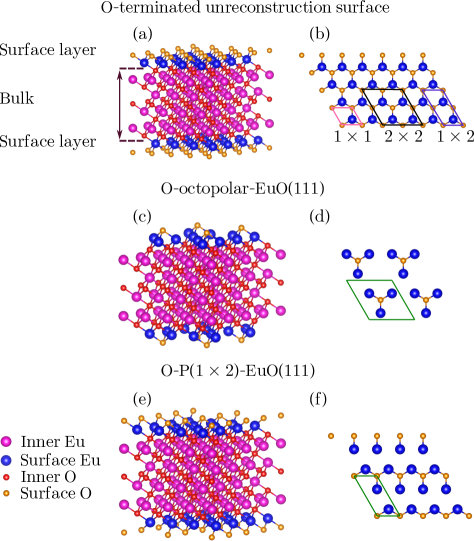
Figure 1 shows the structural models for the two types of surface reconstructions for O-terminated EuO(111). The octopolar reconstruction shown in Figs. 1(c, d) is derived from a 2 2 surpercell of the ideal/unreconstructed EuO(111). Specifically, it is obtained by removing 75% O atoms from the top layer of the surface and removing 25% Eu atoms from the Eu layer underneath the surface oxygen layer. The P(1 2) reconstruction (see Figs. 1(e) and (f)) is built by removing every other oxygen atoms from the surface layer in a 1 2 supercell of the ideal EuO(111). Likewise, the Eu-terminated octopolar structure is obtained by removing 75% surface Eu atoms and 25% O atoms underneath the surface Eu layer. While in the Eu-terminated P(1 2) structure, we remove every other Eu surface atoms in the surface layer of a 1 2 supercell of EuO(111). Hereafter, Eu-octopolar-EuO(111) and O-octopolar-EuO(111) refer to the octopolar-reconstructed EuO(111) with Eu- and O-termination, respectively. While Eu-P(1 2)-EuO(111) and O-P(1 2)-EuO(111) stand for the P(1 2)-reconstructed EuO(111) with Eu- and O-termination, respectively. In our calculations, we consider the surface reconstructions for both sides of the slabs. As a result, we find that Eu-octopolar-EuO(111), O-octopolar-EuO(111) and O-P(1 2)-EuO(111) are semiconducting, except for that the Eu-P(1 2)-EuO(111) shows a half-metal behavior. The calculated band gaps of Eu-octopolar-EuO(111), O-octopolar-EuO(111), and O-P(1 2)-EuO(111) are 0.69 eV, 0.80 eV, and 0.58 eV, respectively. Thus, one may expect that these reconstructed surfaces are more stable than the ideal EuO(111).
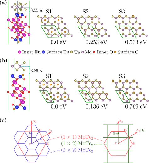
We now turn to the MoTe2/EuO(111) heterostructures, for which the geometric models are shown in Fig. 2. There are two types of heterostructures/interfaces if we classify them according to the surface reconstruction of EuO(111), i.e., MoTe2/octopolar-EuO(111) (Fig. 2(a)) and MoTe2/P(1 2)-EuO(111) (Fig. 2(b)), respectively. Since there is a small lattice mismatch (less than 3%) between the MoTe2 monolayer and the ideal EuO(111), we have the same number of unit cells of MoTe2 and the unreconstructed EuO(111) in the slab models for the heterostructures. Specifically, there is a 2 2 supercell of MoTe2 in the unit cell of MoTe2/octopolar-EuO(111). Likewise, there is a 1 2 supercell of MoTe2 in the unit cell of MoTe2/P(1 2)-EuO(111). For each type of MoTe2/EuO(111) heterostructures, we have considered three types of stacking between the MoTe2 monolayer and EuO(111) substrate for both the O- and Eu-terminated surfaces. These configurations are referred to as S1, S2, and S3, respectively. As an example, we show in Fig. 2(a) the detail of the interface structures of MoTe2/O-terminated-EuO(111). In S1, the hollow site of the MoTe2 monolayer is on the top of the surface O atom. While in S2 (S3), the surface O atom is right below Mo (Te).
The overlayer well preserves its geometric profile upon structural relaxation. And there is no direct chemical bonding between the MoTe2 monolayer and the substrate. The layer distances between Mo and the surface outmost atom for MoTe2/O-octopolar-EuO(111) are 3.55 Å, 4.07 Å, and 4.06 Å for S1, S2, and S3, respectively. While for MoTe2/O-P(1 2)-EuO(111), they are about 3.86 Å, 4.26 Å, 4.41 Å for S1, S2, and S3, respectively. S1 is found to be more stable than the other two configurations for both types of heterostructures. It is 0.253 eV and 0.533 eV lower than S2 and S3 for the octopolar MoTe2/EuO(111), respectively. For the MoTe2/O-P(1 2)-EuO(111), the energy difference between S1 and S2 (S3) is 0.136 eV (0.769 eV).
III.2 Electronic structure of MoTe2/EuO(111)
With the geometric structures, we now proceed to the electronic structure of the MoTe2/EuO(111) heterostructures. Note that there are supercells of MoTe2 in the structural models of the heterostructures, which cause band foldings. To eliminate the folded bands, a band unfolding procedure is necessary. For interfaces like the systems in the present study, we use the layer -projection method as implemented in program KPROJChen and Weinert (2018). In this way, the unfolded bands were obtained by projecting the supercell wavefunctions of the MoTe2 monolayer onto the -points in the Brillouin zone (BZ) of the primitive cell. Fig. 2 (c) shows the BZs for the primitive cell and supercells of the MoTe2 monolayer and corresponding high symmetry points.
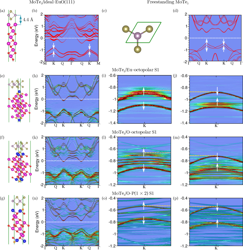
Figure 3 shows the unfolded/-projected bands for the MoTe2 overlayer in MoTe2/EuO(111). We only show the band structure for the lowest-energy configuration for each type of heterostructure, namely, the S1 configurations shown in Fig. 2. We have not attempted calculations of MoTe2/EuO(111) for the substrate with Eu-terminated P(1 2) reconstruction since this type of surface reconstruction is energetically higher than others. The results for the freestanding MoTe2 and MoTe2/ideal-EuO(111) are shown for comparison (Figs. 3(a)-(d)), which are in good agreement with previous studiesQi et al. (2015); Zhang et al. (2016). Figs. 3(e)-(j) and (f)-(n) are for MoTe2/Eu-octopolar-EuO(111) and MoTe2/O-octopolar-EuO(111), respectively. While Figs. 3(g)-(p) are for MoTe2/O-P(1 2)-EuO(111).
One can see from Figs. 3(h), (k) and (n) that the conduction bands of MoTe2 preserve well in the presence of the substrate. For MoTe2/octopolar-EuO(111)(see Figs. 3(e, f)), the Fermi levels move into the conduction band, similar to the heterostructure with ideal EuO(111)Qi et al. (2015); Zhang et al. (2016) (see Fig. 3(b)). However, the Fermi levels of our systems are much closer to the gap than that of MoTe2/unreconstructed-EuO(111). One can see from Figs. 3(h, k) that the Fermi level is about 0.1 eV above the CBM. Whereas, previous studies reveal that it is about 0.4 eV above the CBM for MoTe2/unreconstructed-EuO(111)Qi et al. (2015); Zhang et al. (2016). For MoTe2/P(1 2)-EuO(111), the Fermi level even lies in the gap (see Fig. 3 (n)). Another distinct effect of the surface reconstruction on the electronic structure of MoTe2 is related to the nature of the band gap. In the case of MoTe2/ideal-EuO(111), the overlayer undergoes a direct-indirect band gap transition due to that the strong bonding between MoTe2 and the substrate pushes the point down to a lower energy than the CBM (Fig. 3(b)). In contrast, the direct band gap of the MoTe2 monolayer is maintained upon interfacing with the reconstructed surfaces.
The reconstructed surfaces do have substantial impact on the valleys of the MoTe2 monolayer. In the two panels on the right side of Fig. 3, we show the zoom-in unfolded bands near K and K′. One can see that the spin-up states of the MoTe2 monolayer are modified by the interaction with the substrate states. The reason is that there is a strong spin-dependent hybridization between the states of MoTe2 and the substrate since near the K and K valleys there are mainly the majority (spin-up) states of the substrate (not shown). For MoTe2/O-octopolar-EuO(111), the strong hybridization drives the spin-up band into multiple subbands, so that it is difficult to identify the VBM at K. In this case, we define the state to which the contribution of the MoTe2 monolayer over 50% to be the VBM of it. The spin-dependent interaction breaks the time-reversal symmetry that gives rise to the degeneracy of the electronic bands at K and K′, thus leading to the so called valley polarization. We define the valley polarization as . Here denotes the valence band, represents the valley index. The valley polarizations in our systems are dependent on the surface reconstruction of the substrate and the specific stacking between them. They are about 7.56 meV and 25.62 meV for MoTe2/Eu-octopolar-EuO(111) and MoTe2/O-octopolar-EuO(111), respectively. We have also examined the valley polarization for a different stacking, e.g., S2 in Fig 2(b), for which the valley polarization is about 32.77 meV. For MoTe2/O-P(1 2)-EuO(111), the valley polarization is about 12.07 meV. These valley polarizations are much smaller than that for MoTe2 on the ideal EuO(111), for which it is about 300 meV as reported by previous studiesQi et al. (2015); Zhang et al. (2016). These differences indicate that substrate-surface reconstruction plays an important role in determing the electronic structure of the TMD monolayers.
III.3 Valley polarization in MoTe2/EuO(001)
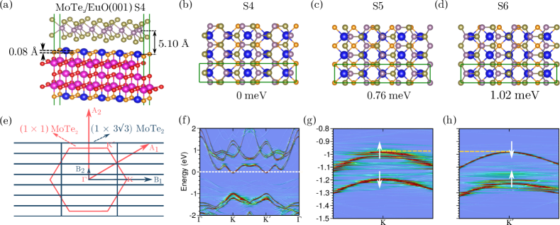
We now discuss the valley polarization in MoTe2/EuO(001). We use a slab consists of five-atomic layers to model EuO(001). One can see from Fig.4(a) that this surface is flat since the Eu and O atoms almost have the same coordinate. Unlike the ideal EuO(111), our DFT calculation of the slab find that EuO(001) is semiconducting. Therefore, the surface reconstruction is not considered in our calculations of MoTe2/EuO(001). Note that EuO(001) and the MoTe2 monolayer have different types of lattice, which requires a large supercell to model the heterostructure. In our model, the MoTe2 monolayer is in a 1 supercell and EuO(001) is in a 1 5 supercell. As a result, the lattice mismatch between them is about 1.91% for the direction and -1.94% for the direction. We have considered three different configurations between the MoTe2 monolayer and EuO(001), which are denoted as S4, S5, and S6, respectively. The geometric structures are shown in Figs. 4(b)-(d). S5 and S6 are obtained by translating the overlayer in S4 by 2.02 Å, 4.10 Å, respectively. The layer distances for these configurations are about 5.10 Å, 5.07 Å, and 5.09 Å for S4, S5, and S6, respectively. These configurations show pretty much similar band structures. Fig. 4(f) depicts the unfolded structure for the MoTe2 monolayer in S4. The Fermi level of this type of heterostructure is closer to the CBM than those for MoTe2/Octopolar-EuO(111). The valley polarization is about 3.17 meV. This value is comparable to that for WSe2/EuSZhao et al. (2017), where the substrate-surface is believed to be the (001) surface. Therefore, the magnetic proximity effect induced by magnetic substrates is surface-orientation dependent.
III.4 Band alignment
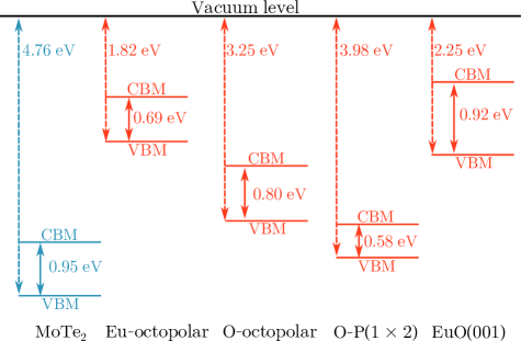
Figure 5 shows the work functions of the isolated systems and the band alignments between the MoTe2 monolayer and various EuO surfaces. One can see that there is a type-II band alignment between the monolayer and O-P(1 2)-EuO(111), which gives rise to the location of the Fermi level right in the band gap. However, the band alignments between MoTe2 and the other surfaces are of type-III, that is, the CBM of the MoTe2 is energetically lower than the VBM of EuO surfaces. Thus, the Fermi levels of their heterostructures move into the conduction band of the MoTe2 monolayer.
III.5 Effective Zeeman field
The valley polarization induced by the magnetic proximity effect can be understood by a low-energy effective modelXiao et al. (2012); Qi et al. (2015); Zhang et al. (2016), for which the Hamiltonian at the K and K′ valleys can be written as:
where denotes the band gap, the spin-orbit interaction strength, the magnetic moment on Mo induced by the substrate and the effective Zeeman field for the valence band. and represent the Pauli matrix and the spin operator, respectively. is the valley index. The effective Zeeman field for the valence band thus can be deduced by the valley polarization, .
| Substrate | Configuration | |||
| S1 | 0.023 | 4.67 | 40.34 | |
| Eu-octopolar | S2 | 0.025 | 7.56 | 65.30 |
| S3 | 0.009 | 0.32 | 2.76 | |
| S1 | 0.042 | 25.62 | 221.31 | |
| O-octopolar | S2 | 0.069 | 43.43 | 375.15 |
| S3 | 0.017 | 3.54 | 30.58 | |
| S1 | 0.024 | 12.07 | 104.26 | |
| O-P | S2 | 0.019 | 32.77 | 283.07 |
| S3 | 0.019 | 38.00 | 328.24 | |
| S4 | 0.078 | 3.17 | 27.38 | |
| EuO(001) | S5 | 0.077 | 3.29 | 28.42 |
| S6 | 0.075 | 3.02 | 26.09 |
Table 1 lists the parameters and obtained from DFT calculations and the estimated for MoTe2/EuO. For MoTe2/EuO(111), is dependent on the detailed interface structures, i.e., surface orientation and specific stacking configuration. is determined by the induced magnetic momentum on Mo, i.e., . Overall, is larger for MoTe2/EuO(001) than for MoTe2/EuO(111). Overall, is larger for MoTe2/EuO(001) than for MoTe2/EuO(111). Compared to those for MoTe2/EuO(111), both and for MoTe2/EuO(001) are insensitive to stacking. The estimated values of for this type of heterostructure is about 27 T, which is much smaller than those for MoTe2/ideal-EuO(111), but comparable to that for WSe2/EuS(001)Zhao et al. (2017). These can be understood since EuO(001) and EuS(001) have the same surface atomic structure and the magnetic moments on the surface Eu atoms are almost the same for them.
In summary, we have investigated the structural and electronic structures of MoTe2/EuO by means of first-principles calculations. We have considered a number of surface reconstructions for the (111) surface of the substrate and find that they have substantial impact on the interface structure. Consequently, the induced valley polarization in MoTe2 by the reconstructed EuO(111) is at least one order of magnitude smaller than that induced by the ideal EuO(111). In addition, the surface reconstructions lead to that the Fermi levels of our systems are about 0.3 eV closer to the VBM than that of MoTe2/ideal-EuO(111). Moreover, we have also studied the valley polarization in MoTe2/EuO(001). For this type of heterostructure, our calculations find that the induced magnetic moments on the Mo atoms and valley polarization are almost the same for the considered stacking configurations. We further estimate the effective Zeeman field induced by the substrate using a low-energy effective Hamiltonian. The estimated effective Zeeman field for MoTe2/EuO(001) is comparable to that for WSe2/EuS(001). Our study reveals that the magnetic proximity effect is strongly dependent on the substrate surface reconstruction and orientation, which may be helpful in understanding recent experiments and designing interfaces for valleytronics.
Acknowledgements.
This work was supported by the National Natural Science Foundation of China (Grants No. 11774084, No. U19A2090, No. 51525202, and No. 11704117) and the Project of Educational Commission of Hunan Province of China (Grant No. 18A003).References
- Butler et al. (2013) S. Z. Butler, S. M. Hollen, L. Cao, Y. Cui, J. A. Gupta, H. R. Gutiérrez, T. F. Heinz, S. S. Hong, J. Huang, A. F. Ismach, E. Johnston-Halperin, M. Kuno, V. V. Plashnitsa, R. D. Robinson, R. S. Ruoff, S. Salahuddin, J. Shan, L. Shi, M. G. Spencer, M. Terrones, W. Windl, and J. E. Goldberger, ACS Nano 7, 2898 (2013), pMID: 23464873.
- Novoselov et al. (2016) K. S. Novoselov, A. Mishchenko, A. Carvalho, and A. H. C. Neto, Science 353 (2016).
- Manzeli et al. (2017) S. Manzeli, D. Ovchinnikov, D. Pasquier, O. V. Yazyev, and A. Kis, Nature Reviews Materials 2, 17033 (2017).
- Xu et al. (2014) X. Xu, W. Yao, D. Xiao, and T. F. Heinz, Nature Physics 10, 343 (2014).
- Wang et al. (2012) Q. H. Wang, K. Kalantarzadeh, A. Kis, J. N. Coleman, and M. S. Strano, Nature Nanotechnology 7, 699 (2012).
- Xiao et al. (2012) D. Xiao, G.-B. Liu, W. Feng, X. Xu, and W. Yao, Phys. Rev. Lett. 108, 196802 (2012).
- Zhu et al. (2011) Z. Y. Zhu, Y. C. Cheng, and U. Schwingenschlögl, Phys. Rev. B 84, 153402 (2011).
- Mak et al. (2012) K. F. Mak, K. He, J. Shan, and T. F. Heinz, Nature Nanotechnology 7, 494 (2012), arXiv:1205.1822 .
- Zeng et al. (2012) H. Zeng, J. Dai, W. Yao, D. Xiao, and X. Cui, Nature Nanotechnology 7, 490 (2012), arXiv:1202.1592 .
- Srivastava et al. (2015) A. Srivastava, M. Sidler, A. Allain, D. Lembke, A. Kis, and A. Imamoglu, Nature Physics 11, 141 (2015).
- Aivazian et al. (2015) G. Aivazian, Z. Gong, A. M. Jones, R. Chu, J. Yan, D. Mandrus, C. Zhang, D. Cobden, W. Yao, and X. Xu, Nature Physics 11, 148 (2015).
- Li et al. (2014) Y. Li, J. Ludwig, T. Low, A. Chernikov, X. Cui, G. Arefe, Y. D. Kim, A. M. van der Zande, A. Rigosi, H. M. Hill, S. H. Kim, J. Hone, Z. Li, D. Smirnov, and T. F. Heinz, Phys. Rev. Lett. 113, 266804 (2014).
- MacNeill et al. (2015) D. MacNeill, C. Heikes, K. F. Mak, Z. Anderson, A. Kormányos, V. Zólyomi, J. Park, and D. C. Ralph, Phys. Rev. Lett. 114, 037401 (2015).
- Qi et al. (2015) J. Qi, X. Li, Q. Niu, and J. Feng, Phys. Rev. B 92, 121403 (2015).
- Zhang et al. (2016) Q. Zhang, S. A. Yang, W. Mi, Y. Cheng, and U. Schwingenschlögl, Advanced Materials 28, 959 (2016).
- Liang et al. (2017) X. Liang, L. Deng, F. Huang, T. Tang, C. Wang, Y. Zhu, J. Qin, Y. Zhang, B. Peng, and L. Bi, Nanoscale 9, 9502 (2017).
- Xu et al. (2018) L. Xu, M. Yang, L. Shen, J. Zhou, T. Zhu, and Y. P. Feng, Phys. Rev. B 97, 041405 (2018).
- Xue et al. (2019) X. Xue, X. Wang, and W. Mi, Journal of Physics D: Applied Physics 52, 115303 (2019).
- Zhou et al. (2019) B. Zhou, Z. Li, J. Wang, X. Niu, and C. Luan, Nanoscale 11, 13567 (2019).
- Yang et al. (2018) G. Yang, J. Li, H. Ma, Y. Yang, C. Li, X. Mao, and F. Yin, Phys. Rev. B 98, 235419 (2018).
- Song et al. (2016) Y. Song, Q. Zhang, W. Mi, and X. Wang, Phys. Chem. Chem. Phys. 18, 15039 (2016).
- Song et al. (2017) Y. Song, X. Wang, and W. Mi, Advanced Electronic Materials 3, 1700245 (2017).
- Ciorciaro et al. (2020) L. Ciorciaro, M. Kroner, K. Watanabe, T. Taniguchi, and A. Imamoglu, Phys. Rev. Lett. 124, 197401 (2020).
- Seyler et al. (2018) K. L. Seyler, D. Zhong, B. Huang, X. Linpeng, N. P. Wilson, T. Taniguchi, K. Watanabe, W. Yao, D. Xiao, M. A. McGuire, K.-M. C. Fu, and X. Xu, Nano Letters 18, 3823 (2018).
- Zhou et al. (2020) W. Zhou, Z. Yang, A. Li, M. Long, and F. Ouyang, Phys. Rev. B 101, 045113 (2020).
- Li et al. (2020) Q. Li, K.-Q. Chen, and L.-M. Tang, Phys. Rev. Applied 13, 014064 (2020).
- Hu et al. (2020) T. Hu, G. Zhao, H. Gao, Y. Wu, J. Hong, A. Stroppa, and W. Ren, Phys. Rev. B 101, 125401 (2020).
- Xie et al. (2018) J. Xie, L. Jia, H. Shi, D. Yang, and M. Si, Japanese Journal of Applied Physics 58, 010906 (2018).
- Zhao et al. (2017) C. Zhao, T. Norden, P. Zhang, P. Zhao, Y. Cheng, F. Sun, J. Parry, P. Taheri, J. Wang, Y. Yang, et al., Nature Nanotechnology 12, 757 (2017).
- Norden et al. (2019) T. Norden, C. Zhao, P. Zhang, R. F. Sabirianov, A. Petrou, and H. Zeng, Nature Communications 10, 1 (2019).
- Wolf (1992) D. Wolf, Phys. Rev. Lett. 68, 3315 (1992).
- Barbier et al. (2000a) A. Barbier, C. Mocuta, H. Kuhlenbeck, K. F. Peters, B. Richter, and G. Renaud, Phys. Rev. Lett. 84, 2897 (2000a).
- Finocchi et al. (2004) F. Finocchi, A. Barbier, J. Jupille, and C. Noguera, Physical Review Letters 92, 136101 (2004).
- Plass et al. (1998) R. Plass, K. Egan, C. Collazo-Davila, D. Grozea, E. Landree, L. D. Marks, and M. Gajdardziska-Josifovska, Phys. Rev. Lett. 81, 4891 (1998).
- Subramanian et al. (2004) A. Subramanian, L. D. Marks, O. Warschkow, and D. E. Ellis, Phys. Rev. Lett. 92, 026101 (2004).
- Barbier et al. (2000b) A. Barbier, C. Mocuta, and G. Renaud, Phys. Rev. B 62, 16056 (2000b).
- Gajdardziska-Josifovska et al. (1991) M. Gajdardziska-Josifovska, P. Crozier, and J. Cowley, Surface Science 248, L259 (1991).
- Pojani et al. (1997) A. Pojani, F. Finocchi, J. Goniakowski, and C. Noguera, Surface Science 387, 354 (1997).
- Zhang and Tang (2008a) W.-B. Zhang and B.-Y. Tang, The Journal of Physical Chemistry C 112, 3327 (2008a).
- Zhang and Tang (2008b) W.-B. Zhang and B.-Y. Tang, The Journal of Chemical Physics 128, 124703 (2008b).
- Franchini et al. (2006) C. Franchini, V. Bayer, R. Podloucky, G. Parteder, S. Surnev, and F. P. Netzer, Phys. Rev. B 73, 155402 (2006).
- Kresse and Furthmüller (1996) G. Kresse and J. Furthmüller, Computational Materials Science 6, 15 (1996).
- Kresse and Furthmüller (1996) G. Kresse and J. Furthmüller, Phys. Rev. B 54, 11169 (1996).
- Blöchl (1994) P. E. Blöchl, Phys. Rev. B 50, 17953 (1994).
- Kresse and Joubert (1999) G. Kresse and D. Joubert, Phys. Rev. B 59, 1758 (1999).
- Perdew et al. (1996) J. P. Perdew, K. Burke, and M. Ernzerhof, Phys. Rev. Lett. 77, 3865 (1996).
- Grimme et al. (2010) S. Grimme, J. Antony, S. Ehrlich, and H. Krieg, The Journal of Chemical Physics 132, 154104 (2010).
- Chen and Weinert (2018) M. Chen and M. Weinert, Phys. Rev. B 98, 245421 (2018).