Dispersive coupling between and a zero-dimensional integrated nanocavity
Abstract
Establishing a coherent interaction between a material resonance and an optical cavity is a necessary first step for the development of semiconductor quantum optics. Here we demonstrate a coherent interaction between the neutral exciton in monolayer and a zero-dimensional, small mode volume nanocavity. This is observed through a dispersive shift of the cavity resonance when the exciton-cavity detuning is decreased, with an estimated exciton-cavity coupling of and a cooperativity of at 80 . This coupled exciton-cavity platform is expected to reach the strong light-matter coupling regime (i.e., with ) at 4 for applications in quantum or ultra-low power nanophotonics.
Introduction
Atomically thin van der Waals (vdW) materials coupled with nanophotonic structures have recently emerged as a promising platform for hybrid integrated photonics [1] due to their easy integration onto a substrate via vdW forces without concern for lattice matching. In particular, the large excitonic binding energy of transition metal dichalcogenides (TMDs) presents an excellent opportunity to study the quantum light-matter interaction in large-scale photonic systems. The first step towards such a quantum system is to demonstrate a coherent interaction between a small mode volume cavity and TMD excitons. To that end, several research groups have observed exciton-polaritons, the manifestation of a coherent interaction between a TMD excitonic transition and a photonic mode. Most of these polaritonic modes have been shown to arise from the strong coupling between two-dimensional (2D) delocalized excitons and bound photonic modes, either obtained with planar microcavities between distributed Bragg reflector (DBR) mirrors [2, 3, 4] or as guided resonances in planar waveguides [5, 6, 7]. Since these photonic modes are spatially extended in 2D, it would be difficult to realize strong polariton-polariton nonlinearities that are inversely proportional to the confinement area [8], an important requirement for photonic quantum simulators [9] and strongly correlated photonic devices [10]. While exciton-polaritons in fiber-DBR cavities [11, 12] can be confined to a small mode volume, such structures emit light out-of-plane which precludes a straightforward means to couple neighboring cavities.
On-chip integrated zero-dimensional (0D) cavities, such as photonic crystal defect resonators, provide a means to confine light in a small mode volume while allowing many such cavities to couple to each other via evanescent fields [13]. In fact, TMDs coupled to photonic crystal cavities have been used to demonstrate optically pumped lasing [14, 15], cavity enhanced electroluminescence [16], and second harmonic generation [17, 18]. TMD hetero-structures have also been integrated with photonic crystal resonators to demonstrate emission enhancement [19] and lasing [20]. However, no conclusive signature of a coherent interaction between TMD excitons and a small mode volume nanocavity has been reported.
In this paper we report the signature of coherent coupling between the neutral exciton in monolayer and a 0D photonic crystal nanocavity made of silicon nitride (SiN). Specifically we observed a dispersive shift in the cavity transmission spectrum as the exciton is temperature-tuned near the cavity resonance. Our efforts extend previous attempts to demonstrate coherent coupling between the TMD exciton and a SiN nanobeam cavity [21] by implementing a clean dry transfer method [22] and recognizing the role of exciton-phonon interactions in the cavity coupled photoluminescence [23]. The extracted exciton-cavity coupling from the dispersive shift is for an estimated cooperativity , in which is the measured intrinsic broadening of the TMD exciton, and is the bare photonic mode linewidth measured without the TMD material. While our experiment probes the coupled system in a dispersive regime, it provides a straightforward path to achieve the strong light-matter coupling regime at 4 , with an anticipated cooperativity of for this material platform.
Results
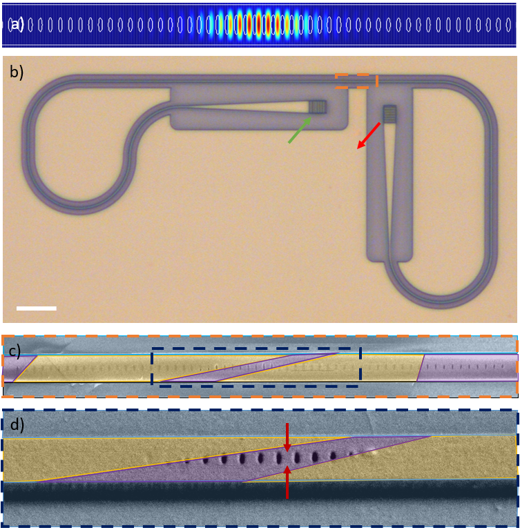
A one-dimensional photonic crystal cavity, also known as a nanobeam resonator, was designed (Fig. 1a) and fabricated (Fig. 1b) in a SiN thin-film on a silicon dioxide substrate with an estimated cavity mode volume , according to the standard cavity QED definition [24]. The bare cavity transmission is interrogated using input and output grating couplers. A monolayer flake was then transferred onto the nanobeam via a modified dry transfer method to eliminate interfering bulk material [22] (Fig. 1c, d). This coupled -nanobeam device was placed in a cryostat where the temperature was swept between and .
Device characterization
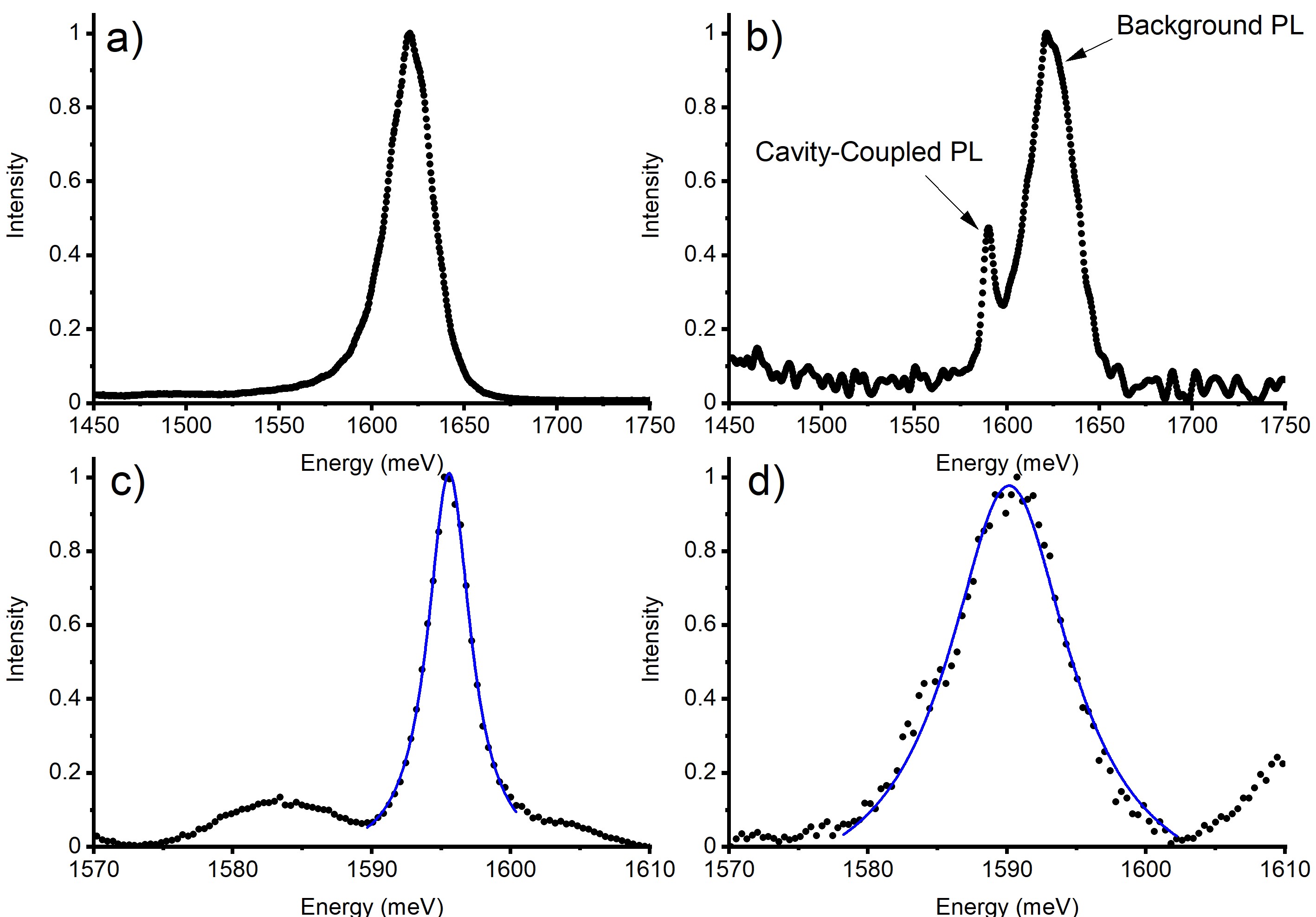
Monolayer exhibits poor optical contrast on the SiN substrate (Fig. 1b). Hence, we confirm the presence of the monolayer on the nanocavity by measuring the photoluminescence (PL) (see Materials and Methods). We observed a strong excitonic peak in the PL spectrum, as shown in Fig. 2a. When the PL is collected from a grating coupler (versus from the full field of view of the confocal microscope), a cavity peak is clearly evidenced in the spectrum (Fig. 2b). The background PL is also observed simultaneously due to imperfect spatial filtering in the confocal microscope. Due to a limited field of view in our microscopy setup, the cavity with transferred monolayer must be in close proximity to the output grating, making the spatial filtering of radiation scattered from the sample difficult.
The nanobeam resonator is characterized via resonant transmission. A broadband super-continuum laser is directed into one of the gratings and the transmitted radiation is collected from the other grating. Prior to monolayer material integration, the cavity resonance was measured at 300 to be with a linewidth , corresponding to a bare quality factor (Fig. 2c). After transfer of the monolayer the bare cavity resonance is measured at 300 to be with a broadened linewidth , corresponding to a loaded quality factor (Fig. 2d). Because the linewidth of the monolayer is the dominant source of decay the observed quality factor of the device is sufficient to probe the physical effect of dispersive coupling.
Temperature dependence
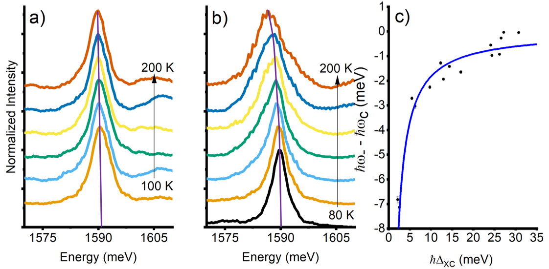
The neutral exciton PL and cavity transmission were then concurrently measured as the temperature was swept from K to K. At low temperature the cavity mode is detuned on the blue side of the excitonic resonance. As the temperature is increased the exciton resonance redshifts, so the detuning between the exciton and cavity resonances decrease. The excitonic PL spectra at different temperatures are fit with a Voigt function [25] to extract the peak energy () and linewidth () where we assume the source of inhomogeneous broadening ( ) is independent of temperature [26].
The temperature dependence of the neutral exciton peak energy is fit to the standard equation for the semiconductor bandgap [27] (Fig. 3a). This relation corresponds to the neutral exciton energy assuming the exciton binding energy is not strongly temperature dependent. In this experiment the temperature range explored remains in the linear regime at high temperatures.
| (1) |
where is the zero Kelvin neutral exciton energy, is a dimensionless coupling constant, and is the average phonon energy. A fit to the extracted energy of the neutral exciton provides a linearized zero Kelvin neutral exciton energy of and a dimensionless coupling constant . These values are comparable to previous reports in the literature [28].
Similarly, the temperature dependence of the neutral exciton linewidth is fit to the Rudin equation [29] (Fig. 3b).
| (2) |
where is the intrinsic homogeneous linewidth, includes exciton interactions with acoustic phonons, includes exciton interactions with longitudinal-optical phonons, and is the average phonon energy. In the linearized equation and where we have assumed . A fit to the extracted neutral exciton linewidth provides for an intrinsic linewidth of and a dimensionless coupling constant . These values are also comparable to previous reports in the literature [26].
It is worth noting the bare nanobeam cavity resonance wavelength does not significantly shift with temperature, which is primarily due to the low thermo-optic coefficient of SiN (Fig. 4a). However, in the TMD-coupled nanobeam resonator a shift in the cavity resonance is clearly observed as the exciton-cavity detuning decreases (Fig. 4b). We attribute this shift to the dispersive coupling of the 2D excitons in the monolayer to the 0D nanobeam cavity mode, which is hereby established via a simple coupled oscillator model.
Coupled Oscillator Model
A homogeneous distribution of TMD excitons and a single 0D cavity mode can be phenomenologically modeled with a Hamiltonian describing two coupled oscillators, wherein the exciton and cavity degrees of freedom coherently interact via an exciton-cavity coupling rate, . The bare oscillator resonance frequencies are measured with respect to a rotating frame at the resonant driving frequency, . The full Hamiltonian is
| (3) |
where and are the detunings of exciton and cavity mode from the laser frequency, respectively; () is the annihilation operator for the exciton (cavity) mode. In the weak excitation regime, exciton saturation and any exciton-exciton interaction can be neglected. Hence, both exciton and cavity operators can be treated as bosonic modes. Including losses, the model can be completed by defining the Liouvillian operator for the density matrix, , which accounts for the finite cavity and exciton linewidths. The Lindblad operators are , in which .
By diagonalizing the Liouvillian within the single excitation subspace the following eigenenergies can be obtained (Supplementary Note 2) [24, 30, 31, 32]
| (4) |
in which is the exciton-cavity detuning. A series expansion of the eigenenergies around infinite detuning, , results in a semi-analytic expression for the cavity peak energy with a far-detuned neutral exciton [33].
| (5) |
As a consequence, the cavity resonance is dependent on the exciton-cavity detuning. The experimental data is fit with Eq. 5 for an exciton-cavity coupling energy (Fig. 4b). It should be noted the exciton PL peak energy is used as a proxy for the absorption resonance, since is known to have a small Stokes shift [12]. The extracted light-matter interaction is similar to related nanophotonic structures, although we expect it to be larger with an optimal coverage of the cavity mode [23].
The light-matter coupling energy was numerically simulated, , from a theoretical formulation of the exciton dipole interacting with the cavity mode electric field [34]. We find that depends on the 2D material extension over the cavity, due to the coupling of a 2D material excitation with a 0D electromagnetic field mode (Supplementary Note 3). Quantitative agreement with the value extracted from the dispersive shift is attained when assuming a 2D flake coverage of the nanocavity compatible with the one inferred from the sample picture (Fig. 1d). A maximal simulated exciton-cavity coupling energy is obtained for this cavity design when the 2D flake extension matches the spatial envelope of the cavity mode electric field.

Discussion
We have estimated the exciton-cavity coupling of a TMD excitonic transition integrated on a zero-dimensional SiN nanobeam cavity. From the known intrinsic linewidth of the neutral exciton of encapsulated in boron nitride ( ) [35], the strong light-matter coupling regime is within reach at 4 . With an improvement in the experimental cavity quality factor to [21], and considering that the simulated exciton-cavity mode coupling energy for an optimal 2D material coverage of the cavity surface is , a low-temperature cooperativity approaching can be anticipated, larger than the state-of-art obtained with single quantum dots [36].
The limiting factor in this material platform is the TMD neutral exciton linewidth, which can be reduced by boron nitride encapsulation [35]. However, there is a trade-off with a reduced field overlap of the cavity mode with the monolayer material due to the increased physical distance from the cavity field maximum. This consequence can be ameliorated by using an air mode cavity [37]. The primary concern with optimization of the cavity design and bare quality factor (without vdW materials) may be design tolerance with respect to cavity perturbations.
An alternative means of integrating the TMD material on the nanocavity without the precision method used here could include large-area transfers using CVD grown monolayers or template stripping methods [38, 39]. Subsequent etching would allow for precise control of the geometry of the vdW material on the nanocavity. This would allow for studies in cavity perturbation theory [40] as well as careful elucidation of the non-linearities inherent to the monolayer neutral exciton [41]. A large-area transfer method would allow for digital tuning of the cavity resonance using an ensemble of cavities instead of tuning the exciton energy via temperature.
Materials and Methods
Design and Fabrication
The nanobeam is made of a thick and a wide silicon nitride film on silicon oxide substrate. The center region of the nanobeam, where the light is confined, consists of 10 tapering elliptical holes, and the reflectors are made of 20 Bragg mirror holes. The minor axis radius of the elliptical holes is fixed to . The tapering region begins with a major axis diameter and a center-to-center distance. The tapering region is quadratically tapered to a major axis radius and a center-to-center distance. The Bragg region remains with fixed values of a major axis radius and a center-to-center distance. The performance of the nanobeam cavity is optimized using Lumerical FDTD solutions software. With these design parameters, we obtain a theoretical resonance at 1639 meV and an intrinsic theoretical Q=25000.
The cavity is fabricated using a 220 thick SiN membrane grown via LPCVD on 4 of thermal oxide on silicon. The samples were obtained from commercial vendor Rogue Valley Microelectronics. A piece of the wafer is spin coated with roughly 400 of Zeon ZEP520A resist. The resist is further coated with a thin layer of Pt/Au which serves as a charge dissipation layer, as both SiN and silicon dioxide are insulators. The resist was then patterned using a JEOL JBX6300FX electron-beam lithography system with an accelerating voltage of 100 . The pattern was transferred to the SiN using a reactive ion etch (RIE) in chemistry. The fabricated sample shows a blue shift of the cavity resonance as compared to the simulated value, as well as significant reduction in the measured Q-factor, which is attributed to fabrication imperfections.
Measurement
The photoluminescence spectrum is measured by exciting the monolayer with a 632 Helium-Neon laser. The resulting emission is collected with a free-space confocal microscopy setup and directed into a Princeton Instruments IsoPlane SCT-320 Imaging Spectrograph. Cavity-coupled photoluminescence spectrum is measured by exciting the monolayer with the same 632 Helium-Neon laser and collecting from a grating coupler with the direct photoluminescence emission occluded by a pinhole in the image plane of the confocal microscope. The transmission spectrum is measured by exciting one of the grating couplers with a supercontinuum laser (Fianium WhiteLase Micro) and collecting from the other grating coupler. Using liquid nitrogen in a continuous flow cryostat (Janis ST-500) the energy of the neutral exciton in the monolayer is shifted with consequent changes in the linewidths.
Acknowledgments
The research was supported by NSF-1845009 and NSF-ECCS-1708579. D.R. is partially supported by a CEI graduate fellowship. A.R. acknowledges support from the IC Postdoctoral Research Fellowship. Part of this work was conducted at the Washington Nanofabrication Facility / Molecular Analysis Facility, a National Nanotechnology Coordinated Infrastructure (NNCI) site at the University of Washington, which is supported in part by funds from the National Science Foundation (awards NNCI-1542101, 1337840 and 0335765), the National Institutes of Health, the Molecular Engineering & Sciences Institute, the Clean Energy Institute, the Washington Research Foundation, the M. J. Murdock Charitable Trust, Altatech, ClassOne Technology, GCE Market, Google and SPTS.
References
- Liu et al. [2019a] Chang-hua Liu, Jiajiu Zheng, Yueyang Chen, Taylor Fryett, and Arka Majumdar. Van der Waals materials integrated nanophotonic devices [Invited]. Optical Materials Express, 9(2):384–399, February 2019a. ISSN 2159-3930. doi: 10.1364/OME.9.000384. URL https://www.osapublishing.org/ome/abstract.cfm?uri=ome-9-2-384. Publisher: Optical Society of America.
- Liu et al. [2015] Xiaoze Liu, Tal Galfsky, Zheng Sun, Fengnian Xia, Erh-chen Lin, Yi-Hsien Lee, Stéphane Kéna-Cohen, and Vinod M. Menon. Strong light–matter coupling in two-dimensional atomic crystals. Nature Photonics, 9(1):30–34, January 2015. ISSN 1749-4893. doi: 10.1038/nphoton.2014.304. URL https://www.nature.com/articles/nphoton.2014.304. Number: 1 Publisher: Nature Publishing Group.
- Dufferwiel et al. [2015] S. Dufferwiel, S. Schwarz, F. Withers, A. a. P. Trichet, F. Li, M. Sich, O. Del Pozo-Zamudio, C. Clark, A. Nalitov, D. D. Solnyshkov, G. Malpuech, K. S. Novoselov, J. M. Smith, M. S. Skolnick, D. N. Krizhanovskii, and A. I. Tartakovskii. Exciton–polaritons in van der Waals heterostructures embedded in tunable microcavities. Nature Communications, 6(1):8579, October 2015. ISSN 2041-1723. doi: 10.1038/ncomms9579. URL https://www.nature.com/articles/ncomms9579. Number: 1 Publisher: Nature Publishing Group.
- Liu et al. [2017a] Xiaoze Liu, Wei Bao, Quanwei Li, Chad Ropp, Yuan Wang, and Xiang Zhang. Control of Coherently Coupled Exciton Polaritons in Monolayer Tungsten Disulphide. Physical Review Letters, 119(2):027403, July 2017a. doi: 10.1103/PhysRevLett.119.027403. URL https://link.aps.org/doi/10.1103/PhysRevLett.119.027403. Publisher: American Physical Society.
- Zhang et al. [2018] Long Zhang, Rahul Gogna, Will Burg, Emanuel Tutuc, and Hui Deng. Photonic-crystal exciton-polaritons in monolayer semiconductors. Nature Communications, 9(1):713, February 2018. ISSN 2041-1723. doi: 10.1038/s41467-018-03188-x. URL https://www.nature.com/articles/s41467-018-03188-x. Number: 1 Publisher: Nature Publishing Group.
- Kravtsov et al. [2020] Vasily Kravtsov, Ekaterina Khestanova, Fedor A. Benimetskiy, Tatiana Ivanova, Anton K. Samusev, Ivan S. Sinev, Dmitry Pidgayko, Alexey M. Mozharov, Ivan S. Mukhin, Maksim S. Lozhkin, Yuri V. Kapitonov, Andrey S. Brichkin, Vladimir D. Kulakovskii, Ivan A. Shelykh, Alexander I. Tartakovskii, Paul M. Walker, Maurice S. Skolnick, Dmitry N. Krizhanovskii, and Ivan V. Iorsh. Nonlinear polaritons in a monolayer semiconductor coupled to optical bound states in the continuum. Light: Science & Applications, 9(1):56, April 2020. ISSN 2047-7538. doi: 10.1038/s41377-020-0286-z. URL https://www.nature.com/articles/s41377-020-0286-z. Number: 1 Publisher: Nature Publishing Group.
- Chen et al. [2020] Yueyang Chen, Shengnan Miao, Tianmeng Wang, Ding Zhong, Abhi Saxena, Colin Chow, James Whitehead, Dario Gerace, Xiaodong Xu, Su-Fei Shi, and Arka Majumdar. Metasurface Integrated Monolayer Exciton Polariton. Nano Letters, June 2020. ISSN 1530-6984. doi: 10.1021/acs.nanolett.0c01624. URL https://doi.org/10.1021/acs.nanolett.0c01624. Publisher: American Chemical Society.
- Verger et al. [2006] A. Verger, C. Ciuti, and I. Carusotto. Polariton quantum blockade in a photonic dot. Phys. Rev. B, 73:193306, May 2006. doi: 10.1103/PhysRevB.73.193306. URL https://link.aps.org/doi/10.1103/PhysRevB.73.193306.
- Angelakis [2017] Dimitris G. Angelakis, editor. Quantum Simulations with Photons and Polaritons: Merging Quantum Optics with Condensed Matter Physics. Quantum Science and Technology. Springer International Publishing, 2017. ISBN 978-3-319-52023-0. doi: 10.1007/978-3-319-52025-4. URL https://www.springer.com/gp/book/9783319520230.
- Gerace et al. [2009] Dario Gerace, Hakan E. Türeci, Atac Imamoglu, Vittorio Giovannetti, and Rosario Fazio. The quantum-optical josephson interferometer. Nature Physics, 5(4):281–284, 2009. doi: 10.1038/nphys1223. URL https://doi.org/10.1038/nphys1223.
- Sidler et al. [2017] Meinrad Sidler, Patrick Back, Ovidiu Cotlet, Ajit Srivastava, Thomas Fink, Martin Kroner, Eugene Demler, and Atac Imamoglu. Fermi polaron-polaritons in charge-tunable atomically thin semiconductors. Nature Physics, 13(3):255–261, March 2017. ISSN 1745-2481. doi: 10.1038/nphys3949. URL https://www.nature.com/articles/nphys3949. Number: 3 Publisher: Nature Publishing Group.
- Gebhardt et al. [2019] Christian Gebhardt, Michael Förg, Hisato Yamaguchi, Ismail Bilgin, Aditya D. Mohite, Christopher Gies, Matthias Florian, Malte Hartmann, Theodor W. Hänsch, Alexander Högele, and David Hunger. Polariton hyperspectral imaging of two-dimensional semiconductor crystals. Scientific Reports, 9(1):13756, September 2019. ISSN 2045-2322. doi: 10.1038/s41598-019-50316-8. URL https://www.nature.com/articles/s41598-019-50316-8. Number: 1 Publisher: Nature Publishing Group.
- Majumdar et al. [2012] Arka Majumdar, Armand Rundquist, Michal Bajcsy, Vaishno D. Dasika, Seth R. Bank, and Jelena Vučković. Design and analysis of photonic crystal coupled cavity arrays for quantum simulation. Physical Review B, 86(19):195312, November 2012. doi: 10.1103/PhysRevB.86.195312. URL https://link.aps.org/doi/10.1103/PhysRevB.86.195312. Publisher: American Physical Society.
- Wu et al. [2015] Sanfeng Wu, Sonia Buckley, John R. Schaibley, Liefeng Feng, Jiaqiang Yan, David G. Mandrus, Fariba Hatami, Wang Yao, Jelena Vučković, Arka Majumdar, and Xiaodong Xu. Monolayer semiconductor nanocavity lasers with ultralow thresholds. Nature, 520(7545):69–72, April 2015. ISSN 1476-4687. doi: 10.1038/nature14290. URL https://www.nature.com/articles/nature14290. Number: 7545 Publisher: Nature Publishing Group.
- Li et al. [2017] Yongzhuo Li, Jianxing Zhang, Dandan Huang, Hao Sun, Fan Fan, Jiabin Feng, Zhen Wang, and C. Z. Ning. Room-temperature continuous-wave lasing from monolayer molybdenum ditelluride integrated with a silicon nanobeam cavity. Nature Nanotechnology, 12(10):987–992, October 2017. ISSN 1748-3395. doi: 10.1038/nnano.2017.128. URL https://www.nature.com/articles/nnano.2017.128. Number: 10 Publisher: Nature Publishing Group.
- Liu et al. [2017b] Chang-Hua Liu, Genevieve Clark, Taylor Fryett, Sanfeng Wu, Jiajiu Zheng, Fariba Hatami, Xiaodong Xu, and Arka Majumdar. Nanocavity Integrated van der Waals Heterostructure Light-Emitting Tunneling Diode. Nano Letters, 17(1):200–205, January 2017b. ISSN 1530-6984. doi: 10.1021/acs.nanolett.6b03801. URL https://doi.org/10.1021/acs.nanolett.6b03801. Publisher: American Chemical Society.
- Fryett et al. [2016] Taylor K. Fryett, Kyle L. Seyler, Jiajiu Zheng, Chang-Hua Liu, Xiaodong Xu, and Arka Majumdar. Silicon photonic crystal cavity enhanced second-harmonic generation from monolayer WSe 2. 2D Materials, 4(1):015031, December 2016. ISSN 2053-1583. doi: 10.1088/2053-1583/4/1/015031. URL https://doi.org/10.1088%2F2053-1583%2F4%2F1%2F015031. Publisher: IOP Publishing.
- Gan et al. [2018] Xue-Tao Gan, Chen-Yang Zhao, Si-Qi Hu, Tao Wang, Yu Song, Jie Li, Qing-Hua Zhao, Wan-Qi Jie, and Jian-Lin Zhao. Microwatts continuous-wave pumped second harmonic generation in few- and mono-layer GaSe. Light: Science & Applications, 7(1):17126–17126, January 2018. ISSN 2047-7538. doi: 10.1038/lsa.2017.126. URL https://www.nature.com/articles/lsa2017126. Number: 1 Publisher: Nature Publishing Group.
- Rivera et al. [2019] Pasqual Rivera, Taylor K. Fryett, Yueyang Chen, Chang-Hua Liu, Essance Ray, Fariba Hatami, Jiaqiang Yan, David Mandrus, Wang Yao, Arka Majumdar, and Xiaodong Xu. Coupling of photonic crystal cavity and interlayer exciton in heterobilayer of transition metal dichalcogenides. 2D Materials, 7(1):015027, December 2019. ISSN 2053-1583. doi: 10.1088/2053-1583/ab597d. URL https://doi.org/10.1088%2F2053-1583%2Fab597d. Publisher: IOP Publishing.
- Liu et al. [2019b] Yuanda Liu, Hanlin Fang, Abdullah Rasmita, Yu Zhou, Juntao Li, Ting Yu, Qihua Xiong, Nikolay Zheludev, Jin Liu, and Weibo Gao. Room temperature nanocavity laser with interlayer excitons in 2D heterostructures. Science Advances, 5(4):eaav4506, April 2019b. ISSN 2375-2548. doi: 10.1126/sciadv.aav4506. URL https://advances.sciencemag.org/content/5/4/eaav4506. Publisher: American Association for the Advancement of Science Section: Research Article.
- Fryett et al. [2018] Taylor K. Fryett, Yueyang Chen, James Whitehead, Zane Matthew Peycke, Xiaodong Xu, and Arka Majumdar. Encapsulated Silicon Nitride Nanobeam Cavity for Hybrid Nanophotonics. ACS Photonics, 5(6):2176–2181, June 2018. doi: 10.1021/acsphotonics.8b00036. URL https://doi.org/10.1021/acsphotonics.8b00036. Publisher: American Chemical Society.
- Rosser et al. [2020a] David Rosser, Taylor Fryett, Abhi Saxena, Albert Ryou, Arka Majumdar, and Arka Majumdar. High-precision local transfer of van der Waals materials on nanophotonic structures. Optical Materials Express, 10(2):645–652, February 2020a. ISSN 2159-3930. doi: 10.1364/OME.383255. URL https://www.osapublishing.org/ome/abstract.cfm?uri=ome-10-2-645. Publisher: Optical Society of America.
- Rosser et al. [2020b] David Rosser, Taylor Fryett, Albert Ryou, Abhi Saxena, and Arka Majumdar. Exciton–phonon interactions in nanocavity-integrated monolayer transition metal dichalcogenides. npj 2D Materials and Applications, 4(1):1–6, July 2020b. ISSN 2397-7132. doi: 10.1038/s41699-020-0156-9. URL https://www.nature.com/articles/s41699-020-0156-9. Number: 1 Publisher: Nature Publishing Group.
- Andreani et al. [1999] Lucio Claudio Andreani, Giovanna Panzarini, and Jean-Michel Gérard. Strong-coupling regime for quantum boxes in pillar microcavities: Theory. Phys. Rev. B, 60:13276–13279, Nov 1999. doi: 10.1103/PhysRevB.60.13276. URL https://link.aps.org/doi/10.1103/PhysRevB.60.13276.
- Olivero and Longbothum [1977] J. J. Olivero and R. L. Longbothum. Empirical fits to the Voigt line width: A brief review. Journal of Quantitative Spectroscopy and Radiative Transfer, 17(2):233–236, February 1977. ISSN 0022-4073. doi: 10.1016/0022-4073(77)90161-3. URL http://www.sciencedirect.com/science/article/pii/0022407377901613.
- Selig et al. [2016] Malte Selig, Gunnar Berghäuser, Archana Raja, Philipp Nagler, Christian Schüller, Tony F. Heinz, Tobias Korn, Alexey Chernikov, Ermin Malic, and Andreas Knorr. Excitonic linewidth and coherence lifetime in monolayer transition metal dichalcogenides. Nature Communications, 7(1):13279, November 2016. ISSN 2041-1723. doi: 10.1038/ncomms13279. URL https://www.nature.com/articles/ncomms13279. Number: 1 Publisher: Nature Publishing Group.
- O’Donnell and Chen [1991] K. P. O’Donnell and X. Chen. Temperature dependence of semiconductor band gaps. Applied Physics Letters, 58(25):2924–2926, June 1991. ISSN 0003-6951. doi: 10.1063/1.104723. URL https://aip.scitation.org/doi/10.1063/1.104723. Publisher: American Institute of Physics.
- Tongay et al. [2012] Sefaattin Tongay, Jian Zhou, Can Ataca, Kelvin Lo, Tyler S. Matthews, Jingbo Li, Jeffrey C. Grossman, and Junqiao Wu. Thermally Driven Crossover from Indirect toward Direct Bandgap in 2D Semiconductors: MoSe2 versus MoS2. Nano Letters, 12(11):5576–5580, November 2012. ISSN 1530-6984. doi: 10.1021/nl302584w. URL https://doi.org/10.1021/nl302584w. Publisher: American Chemical Society.
- Rudin and Reinecke [1990] S. Rudin and T. L. Reinecke. Temperature-dependent exciton linewidths in semiconductor quantum wells. Physical Review B, 41(5):3017–3027, February 1990. doi: 10.1103/PhysRevB.41.3017. URL https://link.aps.org/doi/10.1103/PhysRevB.41.3017. Publisher: American Physical Society.
- Hennessy et al. [2007] K. Hennessy, A. Badolato, M. Winger, D. Gerace, M. Atatüre, S. Gulde, S. Fält, E. L. Hu, and A. Imamoğlu. Quantum nature of a strongly coupled single quantum dot–cavity system. Nature, 445(7130):896–899, 2007. doi: 10.1038/nature05586. URL https://doi.org/10.1038/nature05586.
- Englund et al. [2007] Dirk Englund, Andrei Faraon, Ilya Fushman, Nick Stoltz, Pierre Petroff, and Jelena Vučković. Controlling cavity reflectivity with a single quantum dot. Nature, 450(7171):857–861, December 2007. ISSN 1476-4687. doi: 10.1038/nature06234. URL https://www.nature.com/articles/nature06234. Number: 7171 Publisher: Nature Publishing Group.
- Laussy et al. [2012] Fabrice P. Laussy, Elena del Valle, Michael Schrapp, Arne Laucht, and Jonathan J. Finley. Climbing the Jaynes-Cummings ladder by photon counting. Journal of Nanophotonics, 6(1):061803, November 2012. ISSN 1934-2608, 1934-2608. doi: 10.1117/1.JNP.6.061803. URL https://www.spiedigitallibrary.org/journals/Journal-of-Nanophotonics/volume-6/issue-1/061803/Climbing-the-Jaynes-Cummings-ladder-by-photon-counting/10.1117/1.JNP.6.061803.short. Publisher: International Society for Optics and Photonics.
- Blais et al. [2004] Alexandre Blais, Ren-Shou Huang, Andreas Wallraff, S. M. Girvin, and R. J. Schoelkopf. Cavity quantum electrodynamics for superconducting electrical circuits: An architecture for quantum computation. Physical Review A, 69(6):062320, June 2004. doi: 10.1103/PhysRevA.69.062320. URL https://link.aps.org/doi/10.1103/PhysRevA.69.062320. Publisher: American Physical Society.
- Andreani [2014] Lucio Claudio Andreani. in “Strong Light-Matter Coupling: from atoms to solid state systems”, chapter 2, pages 37–82. World Scientific, Singapore, 2014. doi: 10.1142/9789814460354˙0002. URL https://www.worldscientific.com/doi/abs/10.1142/9789814460354_0002.
- Ajayi et al. [2017] Obafunso A. Ajayi, Jenny V. Ardelean, Gabriella D. Shepard, Jue Wang, Abhinandan Antony, Takeshi Taniguchi, Kenji Watanabe, Tony F. Heinz, Stefan Strauf, X.-Y. Zhu, and James C. Hone. Approaching the intrinsic photoluminescence linewidth in transition metal dichalcogenide monolayers. 2D Materials, 4(3):031011, July 2017. ISSN 2053-1583. doi: 10.1088/2053-1583/aa6aa1. URL https://doi.org/10.1088%2F2053-1583%2Faa6aa1. Publisher: IOP Publishing.
- Najer et al. [2019] Daniel Najer, Immo Söllner, Pavel Sekatski, Vincent Dolique, Matthias C. Löbl, Daniel Riedel, Rüdiger Schott, Sebastian Starosielec, Sascha R. Valentin, Andreas D. Wieck, Nicolas Sangouard, Arne Ludwig, and Richard J. Warburton. A gated quantum dot strongly coupled to an optical microcavity. Nature, 575(7784):622–627, November 2019. ISSN 1476-4687. doi: 10.1038/s41586-019-1709-y. URL https://www.nature.com/articles/s41586-019-1709-y. Number: 7784 Publisher: Nature Publishing Group.
- Quan and Loncar [2011] Qimin Quan and Marko Loncar. Deterministic design of wavelength scale, ultra-high Q photonic crystal nanobeam cavities. Optics Express, 19(19):18529–18542, September 2011. ISSN 1094-4087. doi: 10.1364/OE.19.018529. URL https://www.osapublishing.org/oe/abstract.cfm?uri=oe-19-19-18529. Publisher: Optical Society of America.
- Chen et al. [2017] Jianyi Chen, Xiaoxu Zhao, Sherman J. R. Tan, Hai Xu, Bo Wu, Bo Liu, Deyi Fu, Wei Fu, Dechao Geng, Yanpeng Liu, Wei Liu, Wei Tang, Linjun Li, Wu Zhou, Tze Chien Sum, and Kian Ping Loh. Chemical Vapor Deposition of Large-Size Monolayer MoSe2 Crystals on Molten Glass. Journal of the American Chemical Society, 139(3):1073–1076, January 2017. ISSN 0002-7863. doi: 10.1021/jacs.6b12156. URL https://doi.org/10.1021/jacs.6b12156. Publisher: American Chemical Society.
- Liu et al. [2020] Fang Liu, Wenjing Wu, Yusong Bai, Sang Hoon Chae, Qiuyang Li, Jue Wang, James Hone, and X.-Y. Zhu. Disassembling 2D van der Waals crystals into macroscopic monolayers and reassembling into artificial lattices. Science, 367(6480):903–906, February 2020. ISSN 0036-8075, 1095-9203. doi: 10.1126/science.aba1416. URL https://science.sciencemag.org/content/367/6480/903. Publisher: American Association for the Advancement of Science Section: Report.
- Yang et al. [2015] Jianji Yang, Harald Giessen, and Philippe Lalanne. Simple Analytical Expression for the Peak-Frequency Shifts of Plasmonic Resonances for Sensing. Nano Letters, 15(5):3439–3444, May 2015. ISSN 1530-6984. doi: 10.1021/acs.nanolett.5b00771. URL https://doi.org/10.1021/acs.nanolett.5b00771. Publisher: American Chemical Society.
- Shahnazaryan et al. [2017] V. Shahnazaryan, I. Iorsh, I. A. Shelykh, and O. Kyriienko. Exciton-exciton interaction in transition-metal dichalcogenide monolayers. Physical Review B, 96(11):115409, September 2017. doi: 10.1103/PhysRevB.96.115409. URL https://link.aps.org/doi/10.1103/PhysRevB.96.115409. Publisher: American Physical Society.