Towards Accurate Predictions of Carrier Mobilities and Thermoelectric Performances in 2D Materials
Abstract
The interactions between electrons and lattice vibrational modes play the key role in determining the carrier transport properties, thermoelectric performance and other physical quantities related to phonons in semiconductors. However, for two-dimensional (2D) materials, the widely-used models for carrier transport only consider the interactions between electrons and some specific phonon modes, which usually leads to inaccruate predictions of electrons/phonons transport properties. In this work, comprehensive investigations on full electron-phonon couplings and their influences on carrier mobility and thermoelectric performances of 2D group-IV and V elemental monolayers were performed, and we also analyzed in details the selection rules on electron-phonon couplings using group-theory arguments. Our calculations revealed that, for the cases of shallow dopings where only intravalley scatterings are allowed, the contributions from optical phonon modes are significantly larger than those from acoustic phonon modes in group-IV elemental monolayers, and LA and some specific optical phonon modes contribute significantly to the total intravalley scatterings. When the doping increases and intervalley scatterings are allowed, the intervalley scatterings are much stronger than intravalley scatterings, and ZA/TA/LO phonon modes dominate the intervalley scatterings in monolayer Si, Ge and Sn. The dominant contributions to the total intervalley scatterings are ZA/TO in monolayer P, ZA/TO in monolayer As and TO/LO in monolayer Sb. Based on the thorough investigations on the full electron-phonon couplings, we predict accurately the carrier mobilities and thermoelectric figure of merits in these two elemental crystals, and reveal significant reductions when compared with the calculations based on the widely-used simplified model. Out work not only provides accrurate predictions of carrier transport and thermoelectric performances in these two series of 2D materials by considering full electron-phonon couplings, but also showcases a computational framework for studying related physical quantities in 2D materials.
I Introduction
Two-dimensional (2D) materials offer challenging opportunities for a wide range of applications in nanoscale devices. Among the extraordinary properties in 2D materials, carrier transport properties play the key role in determining the performance in microelectronic, optoelectronic and thermoelectric devices. Extensive studies have been devoted on carrier transport properties in 2D materials, which are dominantly determined by the interaction between electrons and phonons. In the simplest way, the electron-phonon (el-ph) interaction can be understood as originated from the electrostatic potential (known as deformation potential) generated by exciting a phonon in the crystal, which in turn affects all carriers directly. Subsequently, the deformation potential approximation (DPA) method based on the intravalley coupling between electrons and long-wavelength longitudial acoustic (LA) phonon modesLong et al. (2009, 2011), was proposed to estimate or understand the carrier mobilities in many non-polar 2D semiconductors including grapheneXi et al. (2012), phosphoreneQiao et al. (2014) and transition metal dichalcogenide (TMD)Du et al. (2015). However, in some polar or highly anisotropic systems, the DPA method usually misestimates the intrinsic carrier mobility, in which the coupling from the longitudinal optical (LO) phonon modes described as the Frhlich interaction, and the direction-dependent contributions can not be neglected. Furthermore, as previously reportedNakamura et al. (2017); Gunst et al. (2016); Gaddemane et al. (2016), the scatterings from flexural ZA phonons contribute dominantly to the total scattering rates in group-IV elemental monolayers (silicene, germanene, and stanene) due to the lack of -symmetry in buckled honeycomb structure belonging to point group, which also fails the DPA method. Therefore, depending on the specific materials and the situation of the underlying mechanism, systematically computing energy- and momemtum-dependent el-ph interactions is necessary to accurately predict phonon-assisted processes.
Inspired by the extraordinary properties of graphene, the group-IV elemental materials of silicene (Si), germanene (Ge) and stanene (Sn) as the promising alternatives, have attracted tremendous interests. Studies show that such monolayers all possess Dirac fermions similar to graphene, high mechanical flexibility and high electron mobility, leading to the potential applications in batteries and topological devicesPeng et al. (2013); Balendhran et al. (2015). Monolayer Sn was predicted to possess an intrinsic spin-orbit coupling (SOC) gap , which is ideal to realize the quantum spin Hall (QSH) effect at room temperatureXu et al. (2013); van den Broek et al. (2014). Recently, Jian successfully synthesized large-scale and high-quality stanene on Sb (111), providing a good platform to study novel phenomena such as QSH effectGou et al. (2017). In contrast to 2D group-IV materials, 2D group-V elemental materials of phosphorene (P), arsenene (As) and antimonene (Sb) with the same buckled honeycomb structure are semiconductors with wide band gaps, probably leading to the applications in transistors with high on/off ratiosZhu and Tománek (2014) or optoelectric devices operating in the visible rangeZhang et al. (2015). Recent works reported that, the surface plasmon resonance sensor based on -phosphorene/MoS2 heterojunction possesses significantly higher sensitivity compared with conventional or graphene-based SPR sensorsSharma and Pandey (2018), and the monolayer arsenene has the potential to serve as anode materials in high-performance Magnesium-ion batteriesYe et al. (2019). Interestingly, the -antimonene undergoes a transformation from a topological semimetal to a topological insulator at 22 bilayer, then to QSH phase at 8 bilayers and finally to a topological trivial semiconductor at 3 or thinner bilayersZhang et al. (2012).
Herein, based on the first-principles method, we systematically investigate the full el-ph coupling effects in 2D group-IV and V materials. These two series of 2D materials indeed possess a broad range of carrier mobilities, which may lead to various applications. Compared with group-IV counterparts, group-V materials are more buckled, strengthening the overlap of the orbitals, thus may lead to the enhancement of the interaction between the electrons and ZA phonons. The conduction band and valence band for group-V materials are flatter than group-IV materials, which is beneficial to satisfy the energy conservation condition and further increases the el-ph coupling near the Fermi level. To further investigate the roles of different phonon modes, we also derive in details the selection rule for the full el-ph scatterings in these two series of materials. Based on the group-theory analysis, we find that, the LA phonons play a dominant role in the hole scattering in arsenene and antimonene, which is in contrast to the previous report that group-V materials have the same scattering mechanism as group-IV materialsWang et al. (2017). For monolayer phosphorene, arsenene and antimonene, despite the different bands and locations of VBM, LA phonon modes with A irreducible representation (irreps) of C2 group near point dominate the intravalley scatterings due to the identical symmetry and irreps of the intial and final electronic states. However, phosphorene is the only material with degenerate VBM where the intervalley scattering from one VBM to another is dominated by ZA and TA phonon modes. The VBM of monolayer arsenene and antimonene locates at point without degeneracy, hence the intravalley scattering becomes dominant.Finally, by considering the full el-ph scatterings, an accurate prediction of the thermoelectric performances of these two series of materials is achieved.
II Results and Discussion
II.1 Optimized Configurations and Band Structures
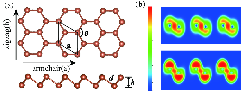
Compared with the planar geometry of graphene, 2D group-IV and V crystals have buckled structure with two sublayers. The top and side views of configurations of the 2D group IV materials (silicene, germanene, stanene) and group V materials (phosphorene, arsenene, antimonene) are shown in Fig. 1(a). The optimized lattice constants , the distance between two sublayers , bond angle and bond length are shown in Table S1 which are consistent with previous reportsMortazavi et al. (2016); Kurpas et al. (2019); Balendhran et al. (2014); Zhang et al. (2017).
In graphene, the orbital is hybridized with and orbitals to form three planar bonds via hybridization, and the remaining orbital forms bonding between adjacent C atoms to guarantee the planarityCahangirov et al. (2009). However, when the bond length increases, the - overlapping decreases and the weaker bonding can not ensure the stability of the planar geometry. By buckling, the planner bonding is dehybridized to form -like hybridization to enhance the overlapping between orbitalsAkturk et al. (2016). Fig. 1(b) shows the calculated electronic localization function (ELF) for silicene and phosphorene. The ELF is a position-dependent function with values ranging from 0 to 1. ELF=1 reflects the maximum probability to find the localized electrons while ELF=0.5 means the electron-gas-like behaviorSILVI and SAVIN (1994). The strength of the bond of 2D group-V materials is much higher than their group-IV counterparts. The one more electron in P, As and Sb increases the degeneracy of electronic states, leading to the unstable state according to the Jahn-Teller theorem, and by a high degree of buckling the degeneracy can be relieved, resulted from the broken symmetryJahn and Teller (1937). Hence, compared with group-IV materials, the group-V counterparts possess larger buckling heights, smaller lattice constants and bond angles, which together increase the overlap of the orbitals.
In order to further investigate the strength of chemical bonding, we also calculate the bulk () and shear moduli () for group-IV and group-V materials, which determine the ductile-brittle nature of materials by Pugh’s ratio Shao et al. (2016). According to Pugh’s rule, a small Pugh’s ratio indicates brittle nature of a material. As shown in Table S1, the Pugh’s ratios for phosphorene, arsenene and antimonene are all lower than their buckled group-IV counterparts, indicating that the high degree of buckling in group-V materials strengthens the bonding. The trend of Pugh’s ratios (Si)(Ge)(Sn) and (P)(As)(Sb) indicates that increasing bond length lowers the bonding strength by decreasing orbital overlap for the same group materials, compensating the effect from the increase of buckling.
The calculated band structures of silicene, germanene, and stanene are shown in Fig. S1(a-c). All these group IV materials are semimetals with a Dirac cone located at the K point, and the SOC effect opens the band gaps of 1.48 meV, 23 meV, 72 meV, respectively. Based on the band structures projected by the atomic orbitals, the band structure near the conduction band minimum (CBM, ) and VBM () are dominantly contributed from orbitals. However, as shown in Fig. S1(d-f), as a comparison, the group V materials are all semiconductors with sizable indirect band gaps. The calculated band gaps without (with) SOC are 1.94 eV (1.94 eV), 1.59 eV (1.47 eV), 1.26 eV (0.99 eV) for phosphorene, arsenene and antimonene respectively. The CBM () locates close to the middle of the -M, which is mainly contributed from and orbitals, and the VBM () locates at point for arsenene and antimonene which is dominantly contributed from and orbitals, while for phosphorene the VBM locates along -K direction mainly contributed by orbitals. The multiple local valleys and peaks, which may play important roles in intervalley el-ph scattering, are labeled as , and , , and their difference from CBM or VBM are shown as , , , in Table S1. For instance, the energy difference between and valleys () is meV in phosphorene.
| Structure | (eV) | (eV) | (eV) | (eV) |
|---|---|---|---|---|
| Si | 1.860 | - | -1.265 | - |
| P | 0.276 | - | -0.049 | -0.162 |
| Ge | 0.511 | - | -0.427 | - |
| As | 0.301 | 0.412 | -0.334 | -0.372 |
| Sn | 0.201 | - | -0.272 | - |
| Sb | 0.252 | 0.293 | -0.437 | -0.466 |
II.2 Full el-ph scatterings: selection rules and carrier mobilities
The calculated carrier mobilities at K along armchair (a) and zigzag (b) directions for these two series of 2D materials, based on the modified DPA theoryLang et al. (2016), are shown in Table S1, accompanied with effective mass , deformation-potential constant , elastic modulus , and the relaxation time defined as , which is determined by the interaction between carriers and LA phonons. The deformation-potential constant reflects the coupling strength of electron and long-wavelength LA phonons, defined as Herring and Vogt (1956), in which is the shift of the VBM and CBM energy level with respect to the lattice deformation . The elastic modulus is related to the interatomic forces. Hence, both and are influenced by the overlap of atomic orbitals. The values of and of 2D group-V materials are higher than their group-IV counterparts due to the enhanced overlap of atomic orbitals by buckling. The obtained mobilities for group-IV materials based on the DPA method are comparable to graphene in the order of , and those of group-V materials are in the range of about . However, as mentioned above, the DPA method may fail for the band-convergence systems such as the group IV and V elemental crystals shown in Fig. S1, therefore the full el-ph scatterings should be investigated to accurately predict the carrier transport properties. According to Eq. (A1), the carrier mobility is mainly determined by the electron velocities and the relaxation times .
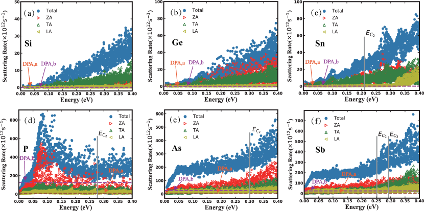
The calculated el-ph scatterings for CBM electrons via acoustic and optical phonon modes for these two series of 2D materials are shown in Fig. 2 and S4 respectively, and the calculated el-ph scatterings for VBM holes via acoustic and optical phonon modes for these two series of 2D materials are shown in Fig. 3 and S5, respectively. All the scattering rates are calculated at 300 K within . Obviously, the calculated scattering rates for group-V materials are much larger than their group-IV counterparts, which is probably resulted from two mechanisms: (i) The enhanced - orbitals overlapping enlarges the el-ph matrix element described in Eq. (A2) due to the stronger sensitivity to the atomic positions. (ii) The band structures of group-V materials near Fermi level are much flatter than the those of group-IV materials, which is more beneficial to satisfy the energy conservation conditions in the scattering processes. Starting from the CBM, with the increase of electronic energy, the scattering rates increase gradually for group-IV materials while dramatically for group-V materials especially for phosphorene, which possesses a wide and nearly flat region near the valley as shown in Fig. S1(d), leading to about 4 times larger in the scattering rate at than those in arsenene and antimonene.
As shown in Fig. 2 and Tables S2-S4, for group-IV elemental monolayers (Si, Ge, Sn) with shallow dopings where only intravalley scatterings are allowed, the intravalley scattering rates for CBM electrons via TO and LO phonon modes are significantly larger than those via acoustic phonon mode, and ZO modes also contribute significantly in monolayer Ge. When the doping increases and intervalley scatterings are allowed, the intervalley scatterings rates surpass the intravalley scatterings, and the contributions from ZA, TA and LO phonon modes dominate the intervalley scatterings. However, the situations for group-V elemental monolayers (P, As, Sb) are different, especially for intravalley scatterings. For intravalley scatterings in monolayer P, the contributions from ZO, LA and TA phonon modes dominate. In monolayer As, the contributions from TO, LO, LA and TA phonon modes dominate, and in monolayer Sb, the contributions from LA, ZO and LO phonon modes dominate. For intervalley scatterings realized by heavy dopings, the contributions from ZA and TO dominate in monolayer P, ZA and TO phonon modes dominate in monolayer As, and TO and LO dominate in monolayer Sb. Furthermore, similar to case in group-IV elemental monolayers, the intervalley scatterings are siginificantly stronger than intravalley scatterings.
In addition, due to the small phonon energies, for monolayer Sn, As and Sb, since the energy of the -valley electrons is well smaller than , only the intravalley and intervalley scatterings between degenerate valleys are possible for small doping. When the energy of -pocket electrons is higher than , - intervalley scattering is allowed, and the scattering rate increases abruptly as a result. In particular, for monolayer Sb, when the energy of pocket electrons is higher than , both - and - intervalley scatterings are allowed, leading to a further increase of the scattering rates, as shown in Fig. 2.
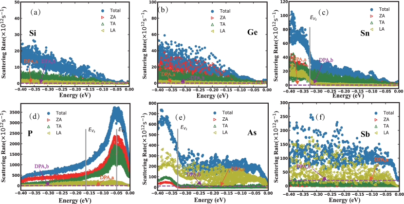
The el-ph scattering rates of -peak holes for these two series of materials at 300 K within are shown in Fig. 3. The behaviors of the scattering rates of holes for silicene and germanene are similar to their electron case. For stanene, as the hole energy descreases to , the scattering rate experiences a sharp rise, implying the activation of - intervalley scatterings. The intravalley and - intervalley scatterings are also allowed for -peak holes with energy lower than , and it is found that, the el-ph scatterings are dominated by ZA and LA phonons in this case, as shown in Fig. 3(c).
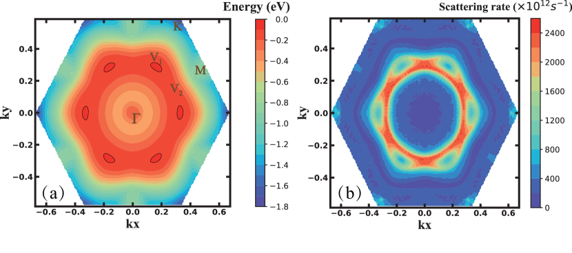
For the hole scatterings in phosphorene, due to the flat valence band near Fermi level, also reflected in the effective mass as listed in Table S1, the scattering rates of -peak holes with energy near Fermi level are ultra-high compared with arsenene and antimonene. When the hole energy is lower than , the - intervalley scattering becomes possible and the scattering rates further increase up to near . Fig. 4(a) shows the contour map of the valence band in Brillouin zone for phosphorene. It is clear that the energy difference between and peaks is rather small, which is beneficial for satisfying the conservation of energy. Fig. 4(b) shows the scattering rates of holes from ZA phonons in the valence band in the Brillouin zone, which reveals that, holes at the junction of the two peaks undergo strong scatterings, due to the typical quadratic dispersion of ZA mode and flat electronic dispersion.
In order to further clarify the underlying mechanisms behind electron-phonon interaction, based on the group-theory analysis, the selection rules in terms of the symmetry of systems for the interaction between phonons and electrons are derived. The electron-phonon interaction depends on the electronic wave functions of the initial states , final states and the coupled phonon with the eigenvector described by the phonon-induced deformation potential Malard et al. (2009); Jiang et al. (2005); Castro Neto and Guinea (2007). Based on the Fermi’s golden rules, in order to calculate the transition probability from initial state to final states of electron or holes via a specific phonon mode, we only need to obtain the core matrix, which could be expressed asChu et al. (2014)
| (1) |
where the perturbation potential , in which is the ion displacement of the atom in the th unit cell, and is the electron coordinate. Therefore, the expression for the selection rules for such transition based on the group theory is written as,
| (2) |
where represents the irreps for electron initial/final states, and denotes the symmetry of the corresponding phonon involved in this process. The involved electrons and phonons must obey the rules of momentum conservation and the compatibility relation among little groups, since they possibly locate at different points in the Brillouin Zone. no null/null means the allowed/forbidden transition channels. Due to the lack of in-plane symmetry in monolayer Si, Ge, Sn of group-IV and monolayer P, As, Sn of group-V, their electronic and phonon symmetry is lowered considerably compared to plane graphene.
As shown in Figure S1, for monolayer Si, Ge and Sn, the hole states in the peak along - and - involved in the intrapeak scatterings transform with the A and B irreps respectively, both belonging to the little group C2. Mathematically, it is allowed for the initial states and final states to belong to the same irreps in the el-ph scattering, i.e. or , but the contribution of such scattering transition is negligible compared to the transition with different irreps for initial and final states in the real systems we studied here. Because, as shown in Figure S1 (a-c), the energy difference of the transition is smaller than that for the transition of or B B, leading to the larger density of states of the former transition, which is beneficial for the el-ph scattering in real systems. Therefore, for intrapeak scattering in monolayer Si, Ge and Sn, we only need to consider the initial and final states transforming with the A and B irreps, i.e. processes. As shown in Tables S9 and S10, in monolayer Si, Ge and Sn, both ZA and TA modes near point transform with the irreps, while LA modes transform with irreps. Hence, restricted by the selection rules shown as Eq. (2), the hole transition from V to V in monolayer Si, Sn and Ge via the out-plane ZA and in-plane TA modes are allowed, due to the non-null of , as shown in Table S9. The analysis based on the selection rules is in good agreement with the numerical results shown as Fig. 3(a-c) and Tables S1-S3.
It should be noticed that, there are some phonon modes near point transforming with the irreps belonging to the little group of CS, but it is reasonable to exclude them since the initial and final states of carriers are with C2 symmetry, which are forbidden to be coupled to the phonon modes with CS group considering the incompatibility relation between and Dresselhaus et al. (2008).
Furthermore, as shown in Figure S6, for the interpeak scatterings of holes in group-IV monolayer materials, since the degenerate VBMs are located at six corners in the Brillouin Zone, there are at least three different interpeak-scattering channels, including the transition to the nearest, next-to-nearest and opposite-side K points. However, the interpeak transition to the next-to-nearest VBMs is actually forbidden since the phonon modes involved are with CS symmetry, which is incompatible to the C2 symmetry. Therefore, only TA modes are allowed restricted by the selection rules and conservation of momentums, as shown in Table S11. The analysis based on the selection rules for holes gives consistent results with previous workNakamura et al. (2017), which reported that ZA and TA are dominant in monolayer Si, Ge and Sn. Moreover, as mentioned above, the Dirac points exist in group-IV materials where the CBM and VBM points touch at the points, therefore, in the same way, the intravalley scatterings of -valley electrons scattered via the ZA and TA phonon modes are allowed, while the intervalley scatterings of electrons between degenerate CBMs via TA modes are allowed. The analysis is shown in Tables S8 and S10.
Similarly, as shown in Figure S7, the CBMs of group-V materials (monolayer P, As and Sb) locate at the points along - with the little group CS, and thus the corresponding irreps of the initial states and final states of CBM are A′. The acoustic phonon modes of ZA, TA and LA near points and along - transform with the A′, A′′ and A′ irreps respectively as shown in Figure S4 (a-c). Therefore, restricted by the selection rules, both ZA and LA modes are allowed in the intravally scatterings of CBM electrons for monolayer P, As and Sb. The analysis is summarized in Table S8. For the intervalley scatterings of electrons between degenerate CBMs, the ZA and LA modes are allowed, as shown in Table S10.
As shown in Figure S7(d-f), the VBMs for monolayer As and Sb locate at the point, while the VBM for monolayer P locates at the middle point along -. The initial and final states of VBM holes for monolayer Sb and As near the point transform with A irreps belonging to the little group C2. However, despite the different location of the VBM for monolayer P, its little-group symmetry and A irreps for VBM are consistent with Sb and As. As shown in Table S9, restricted by the selection rules, only LA modes are allowed in the intrapeak scattering for VBM holes in monolayer P, As and Sb, since the LA phonon is the only mode transforming with the A irreps near the point, as shown in Fig. S4 (a-c), resulted from the non null for the intrapeak transitions.
Nevertheless, for the interpeak scatterings of the VBM holes for monolayer P, As and Sb, the situation is quite different due to the different locations of VBMs. For monolayer As and Sb, since the VBM locates at point, which lacks of degeneracy in the Brillouin Zone, the interpeak scatterings between VBMs no longer exist for the V1-peak holes. As a result, only LA mode dominates the el-ph scatterings of VBM holes for monolayer As and Sb, which is in good agreement with the mode-resolved scattering rates of -peak holes for monolayer As and Sb as shown in Figure 3(e,f) respectively. However, special care should be taken for interpeak scatterings of -peak holes for monolayer P, since the degeneracy of the VBM points in the Brillouin Zone for monolayer P is six, as shown in Figure S6 (d). Three interpeak transitions to the nearest neighboring local VBMs are possible for the -peak holes, and the little groups for the initial and final hole states are . However, the phonon involved in the interpeak transition to the secondly nearest neighboring point transforms with the little group of , incompatible to , therefore this transition is forbidden. Thus, in monolayer P, the transitions of -peak holes to the nearest and the thirdly nearest neighboring local VBM are allowed, and respectively dominated by the TA and ZA phonon modes. The analysis is shown in Figure S6 (d) and Table S11, which is in good agreement with the numerical results shown in Fig. 3(d).
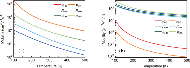
Based on the calculated full el-ph materix elements, the temperature-dependent and mode-resolved relaxation time and the subsequent carrier mobilites along special directions can be calculated according to Eqs. (A1,A2), and the calculated mobilities for these two series of 2D elemental materials are shown in Fig. 5 (a) and (b), respectively. The calculated mobilities at 300K, by a comparison with those calculated by the DPA method are shown in Table S2 as well.By comparison, three distinctions about the carrier mobilities of 2D group-IV and group-V materials can be identified: (1) Generally, the results by the DPA method are overestimated by orders in magnitude due to the only consideration of LA phonons and neglecting the intervalley scattering process; (2) The hole mobilities of group-V materials calculated by these two methods are in roughly good agreement except phosphorene owing to the dominant LA phonons-holes coupling in monolayer -Sb and As; (3) The obvious anisotropy in carrier transport for group-V materials obtained by the DPA method no longer exists in the results considering full el-ph coupling.
II.3 Thermoelectric performance
The thermoelectric (TE) performance of a material is quantified by a dimensionless figure of merit , where represents the Seebeck coefficient, is the electron conductivity, and is the electric/lattice thermal conductivity. High TE performance needs high value of materials with excellent electrical transport properties and poor thermal transport properties simultaneously. However, optimization of values in the TE materials is always challenging due to the inter-correlations of the parameters, and optimizing one leads to deteriorating the other. In recent years, several optimization strategies have been proposed to enhance successfully values in some traditional TE materials and discover new TE materials, and among them, the strategies of the dimension confinement and band convergence attract interests owning to the successful discovery of layered TE materials with extremely high valuesPei et al. (2011); Zhao et al. (2016). Furthermore, considering the appropriate band gaps and heavy atoms in arsenene, stanene and antimonene, high values can be expected in these two series of 2D elemental materials. As reported previouslyChen et al. (2017), antimonene has the value of 2.15 at room temperature and can be further enhanced to 2.90 with strain engineering, based on the DPA and constant relaxation time approximation (CRTA) methods. For arsenene, different constant relaxation times lead to ten times deviation in valuesZhang et al. (2017), implying the importance of the accurate calculations of relaxation time in the values for a material.
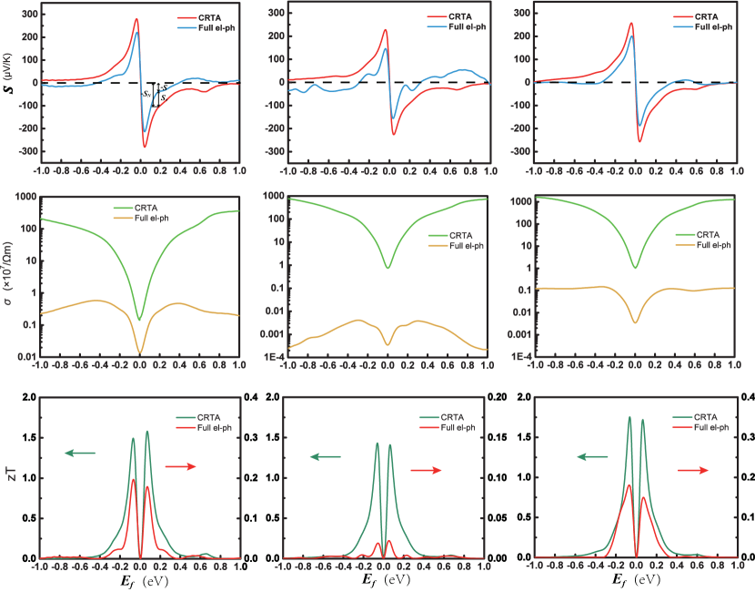
Here, we also calculate the TE and the related transport properties of these two series of 2D elemental crystals by considering full el-ph coupling. Fig. 6(a) shows the calculated Seebeck coeffiecient for the group-IV materials as a function of chemical potential at 300 K using band- and momentum-dependent relaxation times considering full el-ph couplings. For comparison, the results using the CRTA method are also presented. As we know, the behavior of the Seebeck coefficient can be understood by the Mott relationSun et al. (2015); Wei et al. (2015); Liang et al. ,
| (3) |
Where and are the energy-dependent density of states (DOS) and electronic relaxation time, respectively. The Seebeck coefficient can be separated into the band term and the scattering term. A large enhancement of the DOS near the Fermi level leads to a high . The scattering term indicates that is also related to the logarithmic energy derivatives of , which is inversely proportional to the scattering rates. In the CRTA method, the scatterings term is equal to zero considering the definition as shown in Eq. (3).
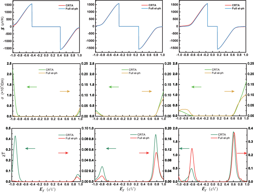
Considering the n-type systems (), the scattering rates of electrons gradually increase as shown in Fig. 2(a-c), therefore the scattering term is positive and considerably large, compared with the zero scattering term in the CRTA method. Moreover, when the scattering term exceeds the band term, even undergoes a sign reversal. Hence, regarding the relaxation time as a constant for group-IV materials brings significant errors to . However, for the group-V materials as shown in Fig. 7(a), the energy-dependent relaxation time influences little on the Seebeck coefficient resulted from the overwhelming band term in the Seebeck coefficient. The maximum Seebeck coefficient of group-V materials is , which is nearly 8 times larger than the group-IV materials and many traditional bulk TE materials including Bi2Te3 ()Poudel et al. (2008), PbTe ()Nielsen et al. (2012), and SnSe ()Zhang and Zhao (2015).
For the electrical conductivity as shown in Fig. 6(b) and Fig. 7(b), near , reaches ,, for silicene, germanene, and stanene respectively, nearly 1, 4 and 3 orders smaller in magnitude than those calculated using the CRTA method respectively. The for n-type group-V materials are nearly overestimated by an order of magnitude. For a -type system, the DPA method gives a better estimation of for arsenene and antimonene compared with phosphorene. As mentioned above, in phosphorene the intervalley scatterings via ZA phonons are strong which fails the DPA method.
The total thermal conductivities is the sum of the electronic contribution and the lattice contribution , i.e. . The electronic thermal conductivity exhibits similar trend with for both DPA and the full el-ph scattering methods. According to the Wiedemann-Franz law, , where is the Lorenz number, increasing leads to the increase of . The lattice thermal conductivities for these two series of 2D elemental crystals are chosen from our previous reports with 28.3 W/mK, 2.4 W/mK, 5.8 W/mK and 106.6 W/mK, 9.0 W/mK, 2.5 W/mK for silicene, germanene, stanene and phosphorene, arsenene, antimonene at 300 K respectivelyPeng et al. (2017).
The results of dimensionless figure of merit are shown in Fig. 6(c) and Fig. 7(c). For group-IV materials, due to the highly overestimated by the CRTA method, despite the relatively small , the maximum value by the CRTA method are in the range of , which is much larger than many traditional thermoelectric materials, e.g. Bi2Te3 ()Poudel et al. (2008), PbTe () Zhang et al. (2013), SnSe () Wang et al. (2015). However, the values for group-V materials predicted by considering full el-ph coupling are only , much smaller than those predicted by using the DPA method. For example, the p-type phosphorene was reported as a good room-temperature thermoelectric material by the CRTA method with , but the value decreases to 0.008 when considering full el-ph coupling. The maximum value at 300 K of antimonene reaches , which is 5 times smaller than the result of 1.88 predicted by the CRTA method. When the temperature rises, the maximum value for antimonene at 700 K reaches 1.3 mainly due to the decrease of the ,which is comparable to PbSe (1.1 at 900 K)Wang et al. (2014), Cu2Se (1.5 at 1000 K)Liu et al. (2012), PbTe (1.64 at 770 K)Ahn et al. (2013).
III Conclusion
In summary, using first principles calculations, we systematically investigate the effects of the electron-phonon couplings in 2D honeycomb group-IV and group-V materials with symmetry. High buckling increases the overlap between orbitals and enhances the interaction between carriers and ZA phonons. The less dispersive band structure of group-V materials further enhance the electron-phonon coupling due to easier satisfaction of energy conservation condition. We find that the symmetry is not a sufficient condition for ZA phonon scattering to dominate. Based on our results of selection rules, the symmetry of transition process only permits LA phonon to be involved in intravalley scattering within VBM in monolayer phosphorus, arsenene and antimonene. However, TA and ZA modes from intervalley scattering between degenerate VBM is dominant in phosphorus and far beyond LA modes. Yet only LA modes dominate in monolayer arsenene and antimonene since no intervalley scattering between VBM at point due to lack of degeneracy. Moreover, we evaluate the TE performance of all these materials with band and momentum relevant relaxation time indicating that the TE properties of a material can be overestimated with constant relaxation-time approximation from DPA calculation.
Numerical Methods
We carry out density functional theory (DFT) using the QUANTUM ESPRESSO codeGiannozzi et al. (2009) with the local density approximation (LDA)Kresse and Furthmuller (1996). Norm-conserving pseudopotentials (NCPP) method with a kinetic energy cutoff of Ry are used to perform the self-consistent DFT calculation. A vacuum space of 28 Å is set along the perpendicular direction to eliminate the interlayer interacions due to the periodic boundary conditions. For the phonon dispersion, the coarse Monkhorst-Pack -mesh and -mesh for all the materials discussed are taken as and respectively. The Wannier interpolation method is used to generate the ultradense fine grid to describe the processes of electron-phonon scattering accurately in the Wannier90Mostofi et al. (2014) and EPW codeNoffsinger et al. (2010); Poncé et al. (2016). Accordingly, much fine and meshes, and can be used to calculate the el-ph coupling matrix guaranteeing the numerical convergence of the intrinsic carrier mobility. In the Boltzmann transport theory, the electron mobility can be defined asXi et al. (2014)
| (A1) |
Where is the number of electrons, and denote the volume of the unit cell and the first Brillouin zone, respectively, is the Fermi-Dirac distribution, is the velocity of the single-particle electron eigenvalue . The interaction between electron and phonon lies in the parameter which is expressed asXi et al. (2014)
| (A2) | ||||
where the sum is over all the final band index for electrons and all the phonon mode index and wavevector . and are the frequency and Bose-Einstein distribution of phonons. and are the electron eigenvalue and the Fermi-Dirac distribution of the final state with band index and wavevector . The electron-phonon matrix element is calculated usingBaroni et al. (2001)
| (A3) |
with and being the initial and final electronic Bloch state, respectively. is the variation of the self-consistent Kohn-Sham (KS) potential experienced by the electrons.
We use BoltzTraP2 code based on the rigid band approach to calculate the transport parameters for arsenene and antimonene monolayersMadsen et al. (2018). The temperature- and doping-dependent electrical transport properties, including carrier concentrations for holes and electrons , electronic conductivity , electronic thermal conductivities and Seebeck coefficient are computed by solving the semiclassical Boltzmann transport equation (BTE), which can be written as Madsen and Singh (2006); Yang et al. (2008); Hong et al. (2016),
| (A4) |
| (A5) |
| (A6) |
| (A7) |
| (A8) |
where is the unit cell volume, is the Fermi-Dirac distribution, is the chemical potential, is the density of states, is the energy dependent conductivity tensor, which can be obtained by , in which N is the number of sampled points and can be calculated by the formulae based on the kinetic theory, i.e. . The velocity of carrier is defined by . In this code, the electron-phonon relaxation time is treated as both energy and direction dependent from Eq.(A2).
Acknowledgement
This work is supported by the National Natural Science Foundation of China under Grants No. 11374063 and 11404348.
References
- Long et al. (2009) Meng-Qiu Long, Ling Tang, Dong Wang, Linjun Wang, and Zhigang Shuai, “Theoretical predictions of size-dependent carrier mobility and polarity in graphene,” Journal of the American Chemical Society 131, 17728–17729 (2009).
- Long et al. (2011) Mengqiu Long, Ling Tang, Dong Wang, Yuliang Li, and Zhigang Shuai, “Electronic structure and carrier mobility in graphdiyne sheet and nanoribbons: Theoretical predictions,” ACS Nano 5, 2593–2600 (2011).
- Xi et al. (2012) Jinyang Xi, Mengqiu Long, Ling Tang, Dong Wang, and Zhigang Shuai, “First-principles prediction of charge mobility in carbon and organic nanomaterials,” Nanoscale 4, 4348 (2012).
- Qiao et al. (2014) Jingsi Qiao, Xianghua Kong, Zhi-Xin Hu, Feng Yang, and Wei Ji, “High-mobility transport anisotropy and linear dichroism in few-layer black phosphorus,” NATURE COMMUNICATIONS 5, 4475 (2014).
- Du et al. (2015) Yongping Du, Huimei Liu, Bo Xu, Li Sheng, Jiang Yin, Chun-Gang Duan, and Xiangang Wan, “Unexpected magnetic semiconductor behavior in zigzag phosphorene nanoribbons driven by half-filled one dimensional band,” Scientific Reports 5, 8921 (2015).
- Nakamura et al. (2017) Yuma Nakamura, Tianqi Zhao, Jinyang Xi, Wen Shi, Dong Wang, and Zhigang Shuai, “Intrinsic charge transport in stanene: Roles of bucklings and electron-phonon couplings,” Advanced Electronic Materials 3, 1700143 (2017).
- Gunst et al. (2016) Tue Gunst, Troels Markussen, Kurt Stokbro, and Mads Brandbyge, “First-principles method for electron-phonon coupling and electron mobility: Applications to two-dimensional materials,” Physical Review B 93, 035414 (2016).
- Gaddemane et al. (2016) Gautam Gaddemane, William G. Vandenberghe, and Massimo V. Fischetti, “Theoretical study of electron transport in silicene and germanene using full-band monte carlo simulations,” in 2016 International Conference on Simulation of Semiconductor Processes and Devices (SISPAD) (IEEE, 2016).
- Peng et al. (2013) Qing Peng, Xiaodong Wen, and Suvranu De, “Mechanical stabilities of silicene,” RSC Advances 3, 13772 (2013).
- Balendhran et al. (2015) Sivacarendran Balendhran, Sumeet Walia, Hussein Nili, Sharath Sriram, and Madhu Bhaskaran, “Elemental analogues of graphene: Silicene, germanene, stanene, and phosphorene,” Small 11, 640–652 (2015), https://onlinelibrary.wiley.com/doi/pdf/10.1002/smll.201402041 .
- Xu et al. (2013) Yong Xu, Binghai Yan, Hai-Jun Zhang, Jing Wang, Gang Xu, Peizhe Tang, Wenhui Duan, and Shou-Cheng Zhang, “Large-gap quantum spin hall insulators in tin films,” Physical Review Letters 111, 136804 (2013).
- van den Broek et al. (2014) B van den Broek, M Houssa, E Scalise, G Pourtois, V V Afanas‘ev, and A Stesmans, “Two-dimensional hexagonal tin:ab initiogeometry, stability, electronic structure and functionalization,” 2D Materials 1, 021004 (2014).
- Gou et al. (2017) Jian Gou, Longjuan Kong, Hui Li, Qing Zhong, Wenbin Li, Peng Cheng, Lan Chen, and Kehui Wu, “Strain-induced band engineering in monolayer stanene on sb(111),” Physical Review Materials 1, 054004 (2017).
- Zhu and Tománek (2014) Zhen Zhu and David Tománek, “Semiconducting layered blue phosphorus: A computational study,” Physical Review Letters 112, 176802 (2014).
- Zhang et al. (2015) Shengli Zhang, Zhong Yan, Yafei Li, Zhongfang Chen, and Haibo Zeng, “Atomically thin arsenene and antimonene: Semimetal-semiconductor and indirect-direct band-gap transitions,” Angew. Chem. Int. Ed. 54, 3112–3115 (2015).
- Sharma and Pandey (2018) Anuj K. Sharma and Ankit Kumar Pandey, “Blue phosphorene/MoS2heterostructure based SPR sensor with enhanced sensitivity,” IEEE Photonics Technology Letters 30, 595–598 (2018).
- Ye et al. (2019) Xiao-Juan Ye, Gui-Lin Zhu, Jin Liu, Chun-Sheng Liu, and Xiao-Hong Yan, “Monolayer, bilayer, and heterostructure arsenene as potential anode materials for magnesium-ion batteries: A first-principles study,” The Journal of Physical Chemistry C 123, 15777–15786 (2019).
- Zhang et al. (2012) PengFei Zhang, Zheng Liu, Wenhui Duan, Feng Liu, and Jian Wu, “Topological and electronic transitions in a sb(111) nanofilm: The interplay between quantum confinement and surface effect,” Physical Review B 85, 201410 (2012).
- Wang et al. (2017) Yangyang Wang, Pu Huang, Meng Ye, Ruge Quhe, Yuanyuan Pan, Han Zhang, Hongxia Zhong, Junjie Shi, and Jing Lu, “Many-body effect, carrier mobility, and device performance of hexagonal arsenene and antimonene,” Chemistry of Materials 29, 2191–2201 (2017).
- Mortazavi et al. (2016) Bohayra Mortazavi, Arezoo Dianat, Gianaurelio Cuniberti, and Timon Rabczuk, “Application of silicene, germanene and stanene for na or li ion storage: A theoretical investigation,” Electrochimica Acta 213, 865–870 (2016).
- Kurpas et al. (2019) Marcin Kurpas, Paulo E. Faria Junior, Martin Gmitra, and Jaroslav Fabian, “Spin-orbit coupling in elemental two-dimensional materials,” Physical Review B 100, 125422 (2019).
- Balendhran et al. (2014) Sivacarendran Balendhran, Sumeet Walia, Hussein Nili, Sharath Sriram, and Madhu Bhaskaran, “Elemental analogues of graphene: Silicene, germanene, stanene, and phosphorene,” Small 11, 640–652 (2014).
- Zhang et al. (2017) Dong-Chen Zhang, Ai-Xia Zhang, San-Dong Guo, and Yi feng Duan, “Thermoelectric properties of beta-as, sb and bi monolayers,” RSC Advances 7, 24537–24546 (2017).
- Cahangirov et al. (2009) S. Cahangirov, M. Topsakal, E. Aktuerk, H. Şahin, and S. Ciraci, “Two- and one-dimensional honeycomb structures of silicon and germanium,” Physical Review Letters 102, 236804 (2009).
- Akturk et al. (2016) E. Akturk, O. Uzengi Akturk, and S. Ciraci, “Single and bilayer bismuthene: Stability at high temperature and mechanical and electronic properties,” PHYSICAL REVIEW B 94, 014115 (2016).
- SILVI and SAVIN (1994) B SILVI and A SAVIN, “CLASSIFICATION OF CHEMICAL-BONDS BASED ON TOPOLOGICAL ANALYSIS OF ELECTRON LOCALIZATION FUNCTIONS,” NATURE 371, 683–686 (1994).
- Jahn and Teller (1937) H. A. Jahn and E. Teller, “Stability of polyatomic molecules in degenerate electronic states - i—orbital degeneracy,” Proceedings of the Royal Society of London. Series A - Mathematical and Physical Sciences 161, 220–235 (1937).
- Shao et al. (2016) Hezhu Shao, Xiaojian Tan, Jun Jiang, and Haochuan Jiang, “First-principles study on the elastic properties of cu2gese3,” EPL (Europhysics Letters) 113, 26001 (2016).
- Lang et al. (2016) Haifeng Lang, Shuqing Zhang, and Zhirong Liu, “Mobility anisotropy of two-dimensional semiconductors,” Physical Review B 94, 235306 (2016).
- Herring and Vogt (1956) Conyers Herring and Erich Vogt, “Transport and deformation-potential theory for many-valley semiconductors with anisotropic scattering,” Phys. Rev. 101, 944–961 (1956).
- Malard et al. (2009) L. M. Malard, M. H. D. Guimarães, D. L. Mafra, M. S. C. Mazzoni, and A. Jorio, “Group-theory analysis of electrons and phonons in -layer graphene systems,” Phys. Rev. B 79, 125426 (2009).
- Jiang et al. (2005) J. Jiang, R. Saito, A. Grüneis, S. G. Chou, Ge. G. Samsonidze, A. Jorio, G. Dresselhaus, and M. S. Dresselhaus, “Intensity of the resonance raman excitation spectra of single-wall carbon nanotubes,” Phys. Rev. B 71, 205420 (2005).
- Castro Neto and Guinea (2007) A. H. Castro Neto and Francisco Guinea, “Electron-phonon coupling and raman spectroscopy in graphene,” Phys. Rev. B 75, 045404 (2007).
- Chu et al. (2014) Yanbiao Chu, Pierre Gautreau, and Cemal Basaran, “Parity conservation in electron-phonon scattering in zigzag graphene nanoribbon,” Applied Physics Letters 105, 347 (2014).
- Dresselhaus et al. (2008) Mildred S. Dresselhaus, Gene Dresselhaus, and Ado Jorio, Group Theory (Springer-Verlag New York, LLC, 2008).
- Pei et al. (2011) Yanzhong Pei, Xiaoya Shi, Aaron LaLonde, Heng Wang, Lidong Chen, and G. Jeffrey Snyder, “Convergence of electronic bands for high performance bulk thermoelectrics,” Nature 473, 66–69 (2011).
- Zhao et al. (2016) Li-Dong Zhao, Cheng Chang, Gangjian Tan, and Mercouri G. Kanatzidis, “Snse: a remarkable new thermoelectric material,” Energy Environ. Sci. 9, 3044–3060 (2016).
- Chen et al. (2017) Kai-Xuan Chen, Shu-Shen Lyu, Xiao-Ming Wang, Yuan-Xiang Fu, Yi Heng, and Dong-Chuan Mo, “Excellent thermoelectric performance predicted in two-dimensional buckled antimonene: A first-principles study,” The Journal of Physical Chemistry C 121, 13035–13042 (2017).
- Sun et al. (2015) Peijie Sun, Beipei Wei, Jiahao Zhang, Jan M. Tomczak, A.M. Strydom, M. Søndergaard, Bo B. Iversen, and Frank Steglich, “Large seebeck effect by charge-mobility engineering,” Nature Communications 6 (2015), 10.1038/ncomms8475.
- Wei et al. (2015) Beipei Wei, Jiahao Zhang, Peijie Sun, Wenquan Wang, Nanlin Wang, and Frank Steglich, “Nernst effect of the intermediate valence compound YbAl3: revisiting the thermoelectric properties,” Journal of Physics: Condensed Matter 27, 105601 (2015).
- (41) Jinghua Liang, Dengdong Fan, Peiheng Jiang, Huijun Liu, and Wenyu Zhao, “Phonon-limited electrical transport properties of intermetallic compound ybal3 from first-principles calculations,” http://arxiv.org/abs/1609.05858v1 .
- Poudel et al. (2008) Bed Poudel, Qing Hao, Yi Ma, Yucheng Lan, Austin Minnich, Bo Yu, Xiao Yan, Dezhi Wang, Andrew Muto, Daryoosh Vashaee, Xiaoyuan Chen, Junming Liu, Mildred S. Dresselhaus, Gang Chen, and Zhifeng Ren, “High-thermoelectric performance of nanostructured bismuth antimony telluride bulk alloys,” SCIENCE 320, 634–638 (2008).
- Nielsen et al. (2012) M. D. Nielsen, E. M. Levin, C. M. Jaworski, K. Schmidt-Rohr, and J. P. Heremans, “Chromium as resonant donor impurity in PbTe,” PHYSICAL REVIEW B 85, 045210 (2012).
- Zhang and Zhao (2015) Xiao Zhang and Li-Dong Zhao, “Thermoelectric materials: Energy conversion between heat and electricity,” Journal of Materiomics 1, 92 – 105 (2015).
- Peng et al. (2017) Bo Peng, Dequan Zhang, Hao Zhang, Hezhu Shao, Gang Ni, Yongyuan Zhu, and Heyuan Zhu, “The conflicting role of buckled structure in phonon transport of 2d group-iv and group-v materials,” Nanoscale 9, 7397 (2017).
- Zhang et al. (2013) Qinyong Zhang, Siqi Yang, Qian Zhang, Shuo Chen, Weishu Liu, Hui Wang, Zhiting Tian, David Broido, Gang Chen, and Zhifeng Ren, “Effect of aluminum on the thermoelectric properties of nanostructured PbTe,” NANOTECHNOLOGY 24, 345705 (2013).
- Wang et al. (2015) Fancy Qian Wang, Shunhong Zhang, Jiabing Yu, and Qian Wang, “Thermoelectric properties of single-layered snse sheet,” Nanoscale 7, 15962–15970 (2015).
- Wang et al. (2014) Heng Wang, Zachary M. Gibbs, Yoshiki Takagiwa, and G. Jeffrey Snyder, “Tuning bands of PbSe for better thermoelectric efficiency,” Energy Environ. Sci. 7, 804–811 (2014).
- Liu et al. (2012) Huili Liu, Xun Shi, Fangfang Xu, Linlin Zhang, Wenqing Zhang, Lidong Chen, Qiang Li, Ctirad Uher, Tristan Day, and G. Jeffrey Snyder, “Copper ion liquid-like thermoelectrics,” Nature Materials 11, 422–425 (2012).
- Ahn et al. (2013) Kyunghan Ahn, Kanishka Biswas, Jiaqing He, In Chung, Vinayak Dravid, and Mercouri G. Kanatzidis, “Enhanced thermoelectric properties of p-type nanostructured PbTe–MTe (m = cd, hg) materials,” Energy & Environmental Science 6, 1529 (2013).
- Giannozzi et al. (2009) Paolo Giannozzi, Stefano Baroni, Nicola Bonini, Matteo Calandra, Roberto Car, Carlo Cavazzoni, Davide Ceresoli, Guido L Chiarotti, Matteo Cococcioni, Ismaila Dabo, Andrea Dal Corso, Stefano de Gironcoli, Stefano Fabris, Guido Fratesi, Ralph Gebauer, Uwe Gerstmann, Christos Gougoussis, Anton Kokalj, Michele Lazzeri, Layla Martin-Samos, Nicola Marzari, Francesco Mauri, Riccardo Mazzarello, Stefano Paolini, Alfredo Pasquarello, Lorenzo Paulatto, Carlo Sbraccia, Sandro Scandolo, Gabriele Sclauzero, Ari P Seitsonen, Alexander Smogunov, Paolo Umari, and Renata M Wentzcovitch, “QUANTUM ESPRESSO: a modular and open-source software project for quantum simulations of materials,” Journal of Physics: Condensed Matter 21, 395502 (2009).
- Kresse and Furthmuller (1996) G Kresse and J Furthmuller, “Efficient iterative schemes for ab initio total-energy calculations using a plane-wave basis set,” PHYSICAL REVIEW B 54, 11169–11186 (1996).
- Mostofi et al. (2014) Arash A. Mostofi, Jonathan R. Yates, Giovanni Pizzi, Young-Su Lee, Ivo Souza, David Vanderbilt, and Nicola Marzari, “An updated version of wannier90: A tool for obtaining maximally-localised wannier functions,” Computer Physics Communications 185, 2309–2310 (2014).
- Noffsinger et al. (2010) Jesse Noffsinger, Feliciano Giustino, Brad D. Malone, Cheol-Hwan Park, Steven G. Louie, and Marvin L. Cohen, “EPW: A program for calculating the electron–phonon coupling using maximally localized wannier functions,” Computer Physics Communications 181, 2140–2148 (2010).
- Poncé et al. (2016) S. Poncé, E.R. Margine, C. Verdi, and F. Giustino, “EPW: Electron–phonon coupling, transport and superconducting properties using maximally localized wannier functions,” Computer Physics Communications 209, 116–133 (2016).
- Xi et al. (2014) Jinyang Xi, Dong Wang, Yuanping Yi, and Zhigang Shuai, “Electron-phonon couplings and carrier mobility in graphynes sheet calculated using the wannier-interpolation approach,” The Journal of Chemical Physics 141, 034704 (2014).
- Baroni et al. (2001) Stefano Baroni, Stefano de Gironcoli, Andrea Dal Corso, and Paolo Giannozzi, “Phonons and related crystal properties from density-functional perturbation theory,” Reviews of Modern Physics 73, 515–562 (2001).
- Madsen et al. (2018) Georg K. H. Madsen, Jesus Carrete, and Matthieu J. Verstraete, “BoltzTraP2, a program for interpolating band structures and calculating semi-classical transport coefficients,” COMPUTER PHYSICS COMMUNICATIONS 231, 140–145 (2018).
- Madsen and Singh (2006) Georg K.H. Madsen and David J. Singh, “Boltztrap. a code for calculating band-structure dependent quantities,” Computer Physics Communications 175, 67–71 (2006).
- Yang et al. (2008) Jiong Yang, Huanming Li, Ting Wu, Wenqing Zhang, Lidong Chen, and Jihui Yang, “Evaluation of half-heusler compounds as thermoelectric materials based on the calculated electrical transport properties,” Advanced Functional Materials 18, 2880–2888 (2008).
- Hong et al. (2016) A. J. Hong, J. J. Gong, L. Li, Z. B. Yan, Z. F. Ren, and J.-M. Liu, “Predicting high thermoelectric performance of abx ternary compounds namgx (x = p, sb, as) with weak electron-phonon coupling and strong bonding anharmonicity,” J. Mater. Chem. C 4, 3281–3289 (2016).