Microscopic Origin of Structural Disorder in : Correlation of Superconductivity and Electronic Structure
Abstract
Rock-salt type niobium nitride () is a well-known superconductor having superconducting transition temperature () 18 K and a large superconducting gap 3 meV. The of thin film exhibits a large scattering irrespective of the growth conditions and lattice parameter. In this work, we investigate the atomic origin of suppression of in thin film by employing combined methods of experiments and ab-initio simulations. Sputtered thin films with different disorder were analyzed through electrical resistivity and x-ray absorption spectroscopy. A strong correlation between the superconductivity and the atomic distortion induced electronic reconstruction was observed. The theoretical analysis revealed that under N-rich growth conditions, atomic and molecular N-interstitial defects assisted by cation vacancies form spontaneously and are responsible for the suppression of in by smearing its electronic densities of states around Fermi level.
Superconducting niobium nitride (NbN) thin films have been extensively used to fabricate modern technological devices like: single photon detector Goltsman et al. (2001), hot electron bolometer Baselmans et al. (2004), Josephson junction Yu et al. (2002), high field superconducting magnet Kampwirth et al. (1985), nano–electromechanical systems and high–pressure devices Blase et al. (2009) etc. The choice of NbN for several technological applications has been motivated due to its relatively higher superconducting transition temperature ( 18 K) and high superconducting energy gap ( 3 meV) among transition metal nitrides (TMNs) Keskar et al. (1971); Kamlapure et al. (2010a). The superior mechanical stability and ease of fabrication of NbN with cost-effective technique such as sputtering is another reason for its popular choice to fabricate devices Kamlapure et al. (2010b). Among its several polymorphs, (space group: ) shows the highest value of owing to its stronger electron-phonon coupling caused by larger electronic densities of states around Fermi energy (EF) and lower Debye temperature () Babu and Guo (2019a); Zou et al. (2016).
One of the crucial issues in the development of superconducting NbN based technology is to achieve the optimum . In the literature, it is well documented that the growth techniques and conditions play a vital role in determining . Polakovic et al. Polakovic et al. (2018) have reported that, as a function of N2 gas pressure shows a dome like behavior with maximum value of 14 K at a specific range of N2 concentration (17-20). Similar results have been reported by Choudhuri et al. Chaudhuri et al. (2010) where of NbN thin films maximizes at certain nitrogen partial pressure. Through Hall measurements Chockalingam et al. Chockalingam et al. (2008) demonstrated that of NbN thin films deposited at different was governed by carrier density caused by Nb and/or N vacancies concentration. However, this work does not shed light on a drastic reduction of the carrier density with samples grown at higher N2 partial pressure (). Similar results have been widely reported in the literature Dane et al. (2017); Shiino et al. (2010); Chand et al. (2009). Often, the atomic disorder has been attributed to the reduction of the in this superconductor Chand et al. (2009); Chockalingam et al. (2009); Carbillet et al. (2020).
Thus, to uncover the microscopic origin of the widely speculated structural disorder and consequently its effect on superconductivity, we synthesize thin films using a dc-magnetron sputtering (details of the deposition parameters are discussed in section I of supplementary material (SM) SI ). Disorder in the films is tuned by varying the during the deposition process. Samples have been thoroughly characterized using complementary characterization tools. A combined approach of experiments and first-principles simulations is adopted to reach the conclusion.
| LP | ||
| (%) | ( 0.006 Å) | (K) |
| 16 | 4.376 | 12.8 |
| 25 | 4.415 | 6.9 |
| 30 | 4.421 | - |
| 65 | 4.486 | - |
| 100 | 4.505 | - |
| Theoretical (this work) | 4.41 | – |
| Experimental Keskar et al. (1971) | 4.40 | 17.3 |
| Theoretical Babu and Guo (2019b) | 4.45 | 18.2 |
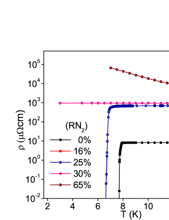
A detailed report on structural and transport characterization of grown films has been published elsewhere Kalal et al. (2020) where XRD result confirms that the sample grown at = 0 is a pure Nb with bcc structure and the sample grown at = 16, 25, 30, 65, 100 have a single phase of NbN with rock-salt type crystal structure (). The (defined as the point where falls down to 10 of its normal value) of the grown films are obtained from standard four probe temperature dependent electrical resistivity () measurements are presented in Fig. 1. The values of , LP and are given in table 1 where a strong correlation between structure and superconductivity is noticed. Here with increase in , the LP is continuously increasing and consequently a reduction in the is seen.
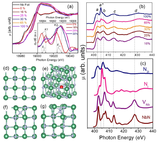
In order to understand the effect of growth conditions on the electronic structure, we performed element specific x-ray absorption near edge spectroscopy (XANES) measurements both at Nb and N K-edges as shown in Fig. 2 (a) and (b), respectively. We note that Nb K-edge splits into two components K1 and K2 (see inset of Fig. 2 (a)). The initial rise K1 is due to the transitions from 1s core level to unoccupied admixed 4d-5p levels while the second absorption rise K2 arises due to transitions from the 1s core level to the Laporte-allowed states of pure 5p symmetry Muller et al. (1978); Agnieszka and Barbara (2012). The absorption edge of sample deposit at = 16 is shifted to higher energy by 3 eV as compared to elemental Nb (see inset of Fig. 2 (a)), which indicates that Nb atom bears positive charge due to the formation of NbN compound. Further, with 25 d band is delocalizing around the Fermi level (EK1).
Similarly, we observed clear changes in the line shape of N K-edge spectra with increase in (see Fig. 2 (b)). A sharp transition at threshold of around 400 eV arises for the sample deposit at = 16. Here, we note presence of electronic sub-band transition levels labeled as a, b, c, d. DOS analysis reveals (see Fig. S2 of SM) these features are results of transition from N-1s core level to unoccupied N-2p orbitals. It is well-known that the TMNs in octahedral bonding coordination (e.g. ) metal d orbitals splits into two electronic sub-bands ( and ) owing to its hybridized characteristics of N-2p orbitals Chen (1997). Feature a (centred at 402.8 eV) in N K-edge XANES spectra is a consequence of hybridized N-2p and level of Nb-4d orbitals, feature b (centered at 406.8 eV) is a consequence of hybridized N-2p and level of Nb-4d orbitals. The feature c and d arises due to higher order hybridization between N-2p and Nb-5s-5p orbitals. Further at = 25, feature b become broad and at = 30, sharp a* feature (404.9 eV) arises in between a and b, whose intensity is gradually increases with increase in .
To identify the atomic origin of above mentioned features, we simulate N K-edge XANES spectra for multiple defect configurations using multi scattering theory (see Fig. S1 of SM SI ). We obtained the relaxed atomic structure of various point defects: (i) isolated N-vacancy (), (ii) multiple N-vacancy (2), (iii) Nb vacancy (), (iv) N interstitial (), (v) N antisite (), (vi) Schottky type defect (), and (vii) interstitial N2 molecules () from SIESTA codes and used them to construct atomic cluster for simulation of ab-initio XANES spectra (computational details of simulations are given in section II of SM SI ). First, to establish the credibility of numerical parameters used in simulations, we obtained N K-edge spectra for pristine . Clearly, features a, b, c, and d are reproduced in simulations. The experimental spectrum obtained for the sample grown at = 16 is in well agreement with the theoretically calculated spectra of having (see Fig. 2 (b) and (c)). A thorough comparison between experimental (Fig. 2 (b)) and simulated (Fig. 2 (c)) XANES spectra of N K-edge, revealed that appearance of a* peak centred around 404.9 eV for the sample grown at higher is probably a signature of either or defects in .
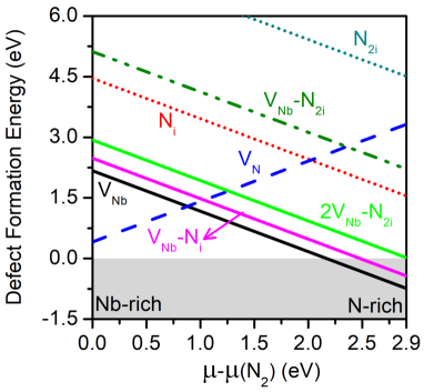
Gall et al. Balasubramanian et al. (2018) studied the energetic of defect formation in TMNs and suggested a cation vacancy () is the most stable defect in , consistent with our estimation of formation energy (FE). FE plot for various defect configurations is shown in Fig. 3. Estimated FE of under N-rich growth condition is -0.74 eV. Work of Gall et al. Balasubramanian et al. (2018) predicted that FE of is very high, which is again consistent with our estimation of high FE = 1.55 eV at N-rich conditions. Further we find even under N-rich conditions, FE of molecular nitrogen () in is very high (4.51 eV). High FE of and in clearly suggests that they will not form spontaneously and their concentration in should be negligible. Interestingly, we find that when and are in a complex form (-) their FE reduces and under N-rich condition, we estimate it to be -0.43 eV (see Fig. 3). Also the estimated binding energy (BE) of - is too high (1.26 eV). The positive BE indicates the preferential stability of the defect complex and higher the magnitude means better the stability (details of method to estimate BE is discussed in section II to SM SI ). Similarly when incorporated near site, it forms - defect complex and its FE is 2.21 eV (see Fig.3). The estimated BE of the- is 1.56 eV. The FE of further reduces to 0.02 eV when it get coupled with two nearest neighbour sites (see Fig.3) with a very high BE of 5.96 eV. These observations clearly establish that the interstitial atomic (N) and molecular nitrogen (N2) can be stabilized in through cation (Nb) vacancies.
Further, we analyze the effect of these defects to the atomic structure of . The obtained relaxed LP of is noted to be 4.41Å. We find that 3.125 of in reduces the unit cell volume by 0.06. While - increases the unit cell volume by 0.025 and defect complex - causes shrinking of unit cell volume by 0.020. A comparison between experimentally obtained LP (and hence volume, see table 1) and theoretically computed volumes suggests that - is predominant in the samples grown with 16 and their concentration increases with increase in . The smaller LP (see table 1) of thin film grown at = 16 suggest a presence of higher concentration of in it. Also the estimated lattice relaxation energy, [= (without ionic relaxation)- (with ionic relaxation)] of with point defects , , , -, , -, and 2- is 15, 10, 102, 107, 163, 160, and 172 meV/atom, respectively. Higher values of for interstitial defects suggest a substantial lattice distortion of , in agreement with the increment of disorder in the films with increase in .
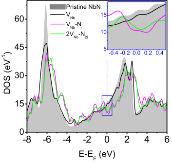
Next, we shall discuss the role of these point defects (if any) on the superconducting properties of thin films. Using the value of electron-phonon coupling constant (), for the strong coupling superconductors can be obtained via McMillan-Allen-Dynes formalism Allen and Dynes (1975); Babu and Guo (2019a); McMillan (1968); Chockalingam et al. (2008), given by:
| (1) |
where is a logarithmic average of phonon frequency, is the averaged screened electron-electron interaction. The further calculated as , where is the atomic mass of atom and is the square of the electron-phonon coupling matrix element averaged over the Fermi surface McMillan (1968); Allen and Dynes (1975). is the electronic density of states at the Fermi level. The can be further approximated as , where is the Debye temperature Liu et al. (2017). From eq. 1, it is quite evident that is sensitive to the . Thus, we computed the electronic DOS of NbN with previously determined dominant defects and presented in Fig. 4. A strong smearing in the electronic structure is visible due to the formation of - or 2- defects complex in (see Fig. 4). DOS calculations shows that of pristine ( supercell) is 16.26 states.eV-1. For 3.125 of , reduces to 14.75 states.eV-1. The computed for - and 2- are 10.50 and 11.15 states.eV-1, respectively. We estimate by substituting the values of (=269 K), (=637 K), (=0.10) computed for in Ref. Babu and Guo, 2019a and the normalized electronic DOS from our simulations in eq. 1. For pristine Gou et al. computed = 18.26 K, a little higher than experimentally obtained ones Babu and Guo (2019a). Using the SIESTA, computed of with 3.125 in eq.1, estimate of to be 15.78 K. The experimental of sample grown at =16 is 12.8 K, hinting concentration of is higher than 3.125 in it. Further using the of - and 2- configurations in eq. 1 results into of 7.18 K and 8.44 K, respectively. These values are in excellent agreement with the experimentally obtained = 6.9 K of sample grown at =25. The absence of superconducting transition (down to 3 K) in the samples grown at 30 is possibly due to the presence of a large disorder in the films, which occurs in films due to the presence of a large concentration of N-interstitial related defects. We estimate a 50 reduction in as compared to the pristine can push the to below 3 K.
Thus, here we unveil the atomic structure of disordered responsible for suppression of superconducting transition temperature. Under N-rich growth conditions, spontaneously formed cation vacancies are responsible for the stabilization of N-interstitial defects in thin films which are otherwise unfavourable with high formation energies. The positive binding energy of the cation vacancies and anion interstitial defect complex further cements their bonding in the crystal. Formation of the N-interstitial defect complex in causes strong smearing of electronic structure by creating atomic disorder in the films and thus a significant reduction in the which strongly influencing the electron-phonon coupling strength and consequently reduces the . Increase in the of vacuum annealed Cukauskas et al. (1989); Carter and Cukauskas (1987); Farrahi et al. (2019) and degradation of superconducting properties at N2 atmosphere Hatano et al. (1988); Oya et al. (2013) further support our proposed mechanism. Based on above analysis we suggest that to obtain with high , films should be grown at Nb-rich conditions to avoid N interstitial defects and annealing of samples in a vacuum is recommended to eliminate residual N atoms.
In summary, we have uncovered the microscopic origin of growth parameter dependence on the of . By probing the electronic structure of disordered samples, we identify point defect complexes consisting of cation vacancies with atomic anion interstitial [-] and cation vacancies with interstitial molecular nitrogen [n-] are responsible for suppression of the in NbN films grown at higher nitrogen partial pressure (). The suppression of the is caused by smearing of electronic structure and reduction of electronic DOS around Fermi energy due to the formation of point defect complex. We show that stabilization of atomic and molecular nitrogen in is assisted by cation vacancies. Estimated of with dominant defects identified from first-principles simulations are in good agreement with the experimentally obtained values.
Acknowledgments
We thank L. Behera, R. Sah and A. Wadikar for technical help provided in experiments. We are thankful to A. K. Sinha, Alok Banerjee, and D. M. phase for support and encouragement. This work is supported through India-DESY project.
References
- Goltsman et al. (2001) G. Goltsman, O. Okunev, G. Chulkova, A. Lipatov, A. Semenov, K. Smirnov, B. Voronov, A. Dzardanov, C. Williams, and R. Sobolewski, Applied physics letters 79, 705 (2001).
- Baselmans et al. (2004) J. J. Baselmans, M. Hajenius, J. Gao, T. Klapwijk, P. De Korte, B. Voronov, and G. Goltsman, Applied physics letters 84, 1958 (2004).
- Yu et al. (2002) Y. Yu, S. Han, X. Chu, S.-I. Chu, and Z. Wang, Science 296, 889 (2002).
- Kampwirth et al. (1985) R. Kampwirth, D. Capone, K. Gray, and A. Vicens, IEEE Transactions on Magnetics 21, 459 (1985).
- Blase et al. (2009) X. Blase, E. Bustarret, C. Chapelier, T. Klein, and C. Marcenat, Nature materials 8, 375 (2009).
- Keskar et al. (1971) K. Keskar, T. Yamashita, and Y. Onodera, Japanese Journal of Applied Physics 10, 370 (1971).
- Kamlapure et al. (2010a) A. Kamlapure, M. Mondal, M. Chand, A. Mishra, J. Jesudasan, V. Bagwe, L. Benfatto, V. Tripathi, and P. Raychaudhuri, Applied Physics Letters 96, 072509 (2010a).
- Kamlapure et al. (2010b) A. Kamlapure, M. Mondal, M. Chand, A. Mishra, J. Jesudasan, V. Bagwe, L. Benfatto, V. Tripathi, and P. Raychaudhuri, Applied Physics Letters 96, 072509 (2010b).
- Babu and Guo (2019a) K. R. Babu and G.-Y. Guo, Physical Review B 99, 104508 (2019a).
- Zou et al. (2016) Y. Zou, X. Qi, C. Zhang, S. Ma, W. Zhang, Y. Li, T. Chen, X. Wang, Z. Chen, D. Welch, et al., Scientific reports 6, 22330 (2016).
- Polakovic et al. (2018) T. Polakovic, S. Lendinez, J. E. Pearson, A. Hoffmann, V. Yefremenko, C. L. Chang, W. Armstrong, K. Hafidi, G. Karapetrov, and V. Novosad, APL Materials 6, 076107 (2018).
- Chaudhuri et al. (2010) S. Chaudhuri, M. Nevala, T. Hakkarainen, T. Niemi, and I. Maasilta, IEEE transactions on applied superconductivity 21, 143 (2010).
- Chockalingam et al. (2008) S. Chockalingam, M. Chand, J. Jesudasan, V. Tripathi, and P. Raychaudhuri, Physical Review B 77, 214503 (2008).
- Dane et al. (2017) A. E. Dane, A. N. McCaughan, D. Zhu, Q. Zhao, C.-S. Kim, N. Calandri, A. Agarwal, F. Bellei, and K. K. Berggren, Applied Physics Letters 111, 122601 (2017).
- Shiino et al. (2010) T. Shiino, S. Shiba, N. Sakai, T. Yamakura, L. Jiang, Y. Uzawa, H. Maezawa, and S. Yamamoto, Superconductor Science and Technology 23, 045004 (2010).
- Chand et al. (2009) M. Chand, A. Mishra, Y. Xiong, A. Kamlapure, S. Chockalingam, J. Jesudasan, V. Bagwe, M. Mondal, P. Adams, V. Tripathi, et al., Physical Review B 80, 134514 (2009).
- Chockalingam et al. (2009) S. Chockalingam, M. Chand, J. Jesudasan, V. Tripathi, and P. Raychaudhuri, in Journal of Physics: Conference Series, Vol. 150 (IOP Publishing, 2009) p. 052035.
- Carbillet et al. (2020) C. Carbillet, V. Cherkez, M. Skvortsov, M. Feigel’man, F. Debontridder, L. Ioffe, V. Stolyarov, K. Ilin, M. Siegel, C. Noûs, et al., Physical Review B 102, 024504 (2020).
- (19) “Supplemental material for- Microscopic Origin of Structural Disorder in : Correlation between Superconductivity and Electronic Structure, providing experimental, computational details” .
- Babu and Guo (2019b) K. R. Babu and G.-Y. Guo, Physical Review B 99, 104508 (2019b).
- Kalal et al. (2020) S. Kalal, M. Gupta, and R. Rawat, Journal of Alloys and Compounds , 155925 (2020).
- Muller et al. (1978) J. Muller, O. Jepsen, O. K. Andersen, and J. Wilkins, Physical Review Letters 40, 720 (1978).
- Agnieszka and Barbara (2012) W. Agnieszka and K. Barbara, Journal of Non-Crystalline Solids 358, 969 (2012).
- Chen (1997) J. G. Chen, Surface Science Reports 30, 1 (1997).
- Balasubramanian et al. (2018) K. Balasubramanian, S. V. Khare, and D. Gall, Acta Materialia 159, 77 (2018).
- Allen and Dynes (1975) P. Allen and R. Dynes, Journal of Physics C: Solid State Physics 8, L158 (1975).
- McMillan (1968) W. L. McMillan, Physical Review 167, 331 (1968).
- Liu et al. (2017) L. Liu, X. Wu, R. Wang, X. Nie, Y. He, and X. Zou, Crystals 7, 111 (2017).
- Cukauskas et al. (1989) E. J. Cukauskas, S. Qadri, and W. L. Carter, Journal of applied physics 65, 2053 (1989).
- Carter and Cukauskas (1987) W. Carter and E. Cukauskas, IEEE Transactions on Magnetics 23, 847 (1987).
- Farrahi et al. (2019) T. Farrahi, M. E. Cyberey, M. B. Eller, and A. W. Lichtenberger, IEEE Transactions on Applied Superconductivity 29, 1 (2019).
- Hatano et al. (1988) M. Hatano, T. Nishino, and U. Kawabe, Journal of Vacuum Science & Technology A: Vacuum, Surfaces, and Films 6, 2381 (1988).
- Oya et al. (2013) G. Oya, Y. Onodera, and Y. Muto, Low Temperature Physics-LT 13 3, 399 (2013).