The drag of photons by electric current in quantum wells
Abstract
The flow of electric current in quantum well breaks the space inversion symmetry, which leads to the dependence of the radiation transmission on the relative orientation of current and photon wave vector, this phenomenon can be named current drag of photons. We have developed a microscopic theory of such an effect for intersubband transitions in quantum wells taking into account both depolarization and exchange-correlation effects. It is shown that the effect of the current drag of photons originates from the asymmetry of intersubband optical transitions due to the redistribution of electrons in momentum space. We show that the presence of dc electric current leads to the shift of intersubband resonance position and affects both transmission coefficient and absorbance in quantum wells.
I Introduction
A wide variety of optical and transport phenomena can be observed in semiconductor structures. Often the determining factor in whether a particular phenomenon can be observed in a specific structure is the symmetry of this structure. The presence of heterointerfaces in nanostructures by itself leads to a reduction of spatial symmetry in comparison with bulk materials Ivchenko and Pikus (1997), and allows the emergence of new effects absent in bulk semiconductors. The symmetry of the structure can be further controlled and lowered in various ways, e.g. deformation, a gradient of temperature, magnetic field, or dc electric current. The latter can lead to a number of electro-optical effects, such as current-induced optical activity Vorob’ev et al. (1979); Tate et al. (2015) or second harmonic generation Lee et al. (1967); Khurgin (1995); Ruzicka et al. (2012); An et al. (2014), which are observed both in bulk and low-dimensional structures.
In the present manuscript, we theoretically study the variation of the refractive index induced by dc electric current linear in current amplitude for the resonant optical transition between subbands in quantum well. The in-plane electric current in quantum well breaks inversion-symmetry and leads to nonequivalence of direction along and against the current. As a result of this, the dielectric function of the quantum well can change depending on the orientation of the radiation wave vector with respect to the current direction. This phenomenon is the opposite to the well-known photon drag effect of electrons: the generation of a direct electric current caused by the absorption of radiation due to the transfer of photon momentum to the free charge carriers. Photon drag effect was widely studied in both bulk semiconductors Gibson et al. (1970); Danishevskii et al. (1970); Ganichev and Prettl (2005); Shalygin et al. (2017) and quantum wells Luryi (1987); A. Grinberg and Luryi (1988); Ganichev et al. (2002); Shalygin et al. (2007); Stachel et al. (2014) and used for characterization of semiconductor structures kinetic properties as well as ultrafast infrared detectors Rogalski (2010); Ganichev and Prettl (2005). By analogy, the effect under study can be named the current drag of photons (CDOP), since optical path length of radiation transmitted through quantum well changes in presence of dc current as if photons are “dragged” by electrons. A similar phenomenon caused by hole current at the optical transition between light-hole and heavy-hole subbands was previously discovered in bulk Ge Vorob’ev et al. (2000).
II Microscopic model
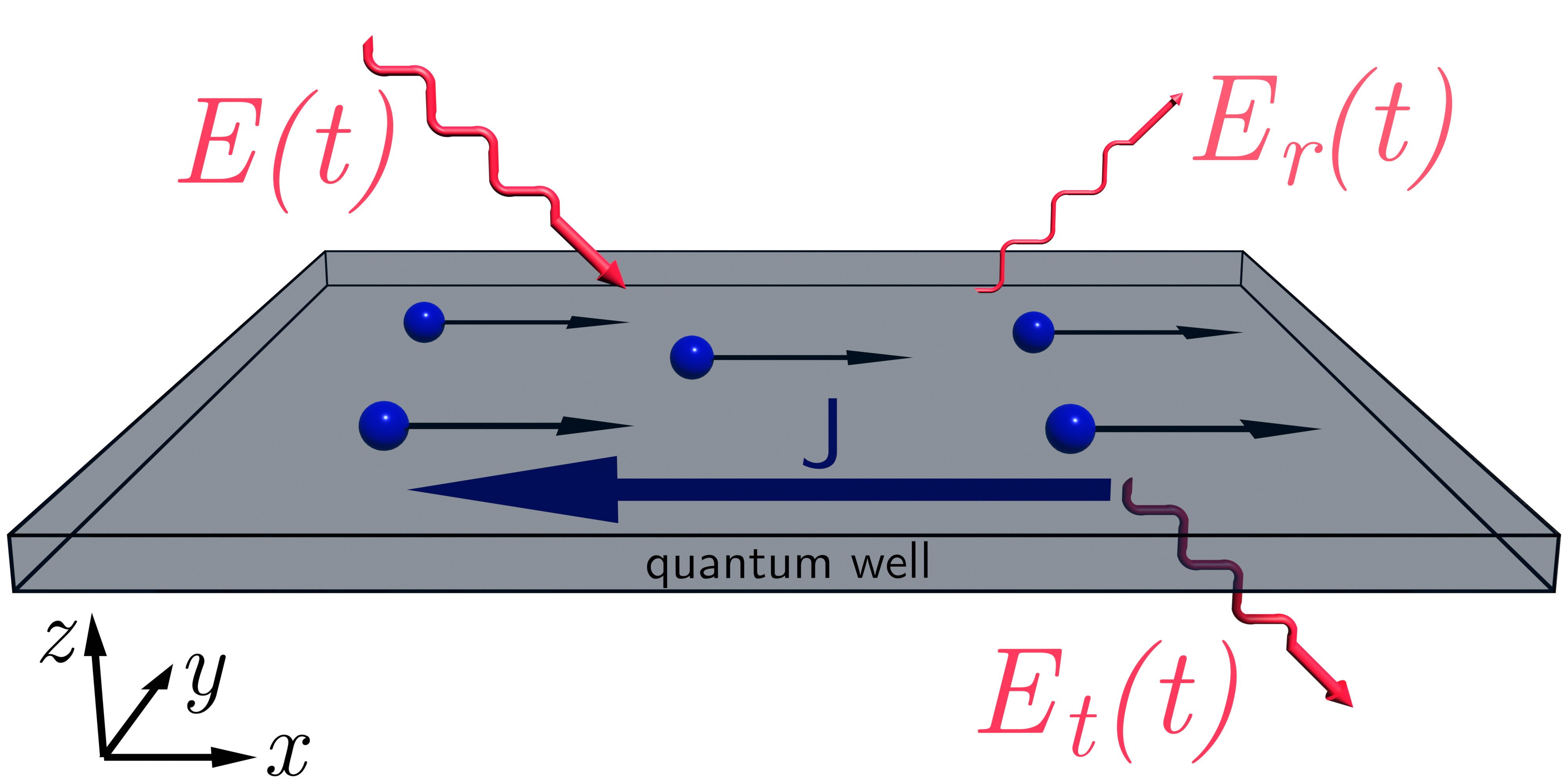
We start with the microscopic model to demonstrate physics behind the CDOP. The geometry of the problem is shown in Fig. 1. We consider direct optical transitions between the first and second subbands of the quantum well. For such transitions, the radiation frequency typically is in the infrared region. Direct intersubband optical transitions are induced by the oblique and p-polarized incident radiation, so its electric field has both in-plane and perpendicular to the quantum well components. Dc electric current affects the radiation transition through the quantum well, which results in the dependence of the and on the current magnitude and direction for the fixed angle of incidence. To explain the reason for this dependence, we first turn to a formal description of the electronic states in the quantum well.
The Hamiltonian of electron in quantum well is given by
| (1) |
where is the electron effective mass, is barrier potential. The solution of this well-known Shrödinger equation gives a series of electron subbands energies with corresponding wave functions , in coordinate representation
where is in-plane electron wave vector and is the surface area of the quantum well.
Radiation induces dipole moment along -direction in quantum well oscillating with the frequency of the incident electromagnetic wave. Dipole moment density along -direction is given by
| (2) |
where is electron distribution function and contribution from individual transitions of electrons with initial state in the first subband with wave vector and final state in the second subband with wave vector . For the direct optical transition the initial electron wave vector differs from the final by the in-plane component of radiation wave vector due to in-plane momentum conservation law. The contributions to the dipole moment induced by optical transitions is proportional to
| (3) |
where is matrix element of coordinate between first and second subband, is electron charge, is photon energy and is optical transition dephasing rate. The difference between initial energy of electron and final is given by
| (4) |
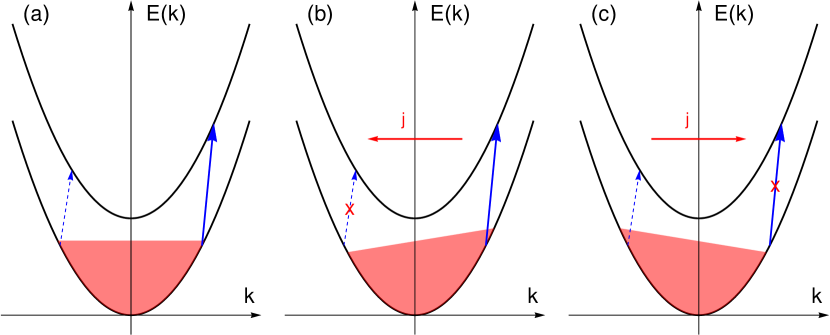
where is energy difference between the ground and second subbands, we assume that linewidth is much smaller than . Last term of the right-hand side of Eq. (4) shows that the contribution of the transition to the depends on the relative direction of wave vectors and . If we set the direction of along -axis the values of will depend on the sign of which is schematically shown in Fig. 2(a) by thick and dashed blue arrows, thus there is a definite asymmetry of optical transitions.
The physics behind CDOP can be most clearly demonstrated for the case of low temperatures for degenerated electron gas described by the Fermi step function. Dc current leads to the redistribution of electrons in -space, thus the current along -direction turns off optical transition with positive electron wave vectors close to the Fermi energy due to the depopulating of states (see Fig. 2(b)), current with opposite direction, on the other hand, turns off transition with negative electron wave vectors (see Fig. 2(c)). As a result dipole momentum density given by Eq. (2) changes with the change of the current direction, which leads to the fact that phase shift and amplitude of the electric field of the transmitted radiation depends on the relative direction of the radiation wave vector and electric current in quantum well.
III Theory
Now we turn to the detailed theory of the effect. The Hamiltonian of the electrons excited by electromagnetic wave is given by
| (5) |
where is perturbation induced by incident radiation. By solving equation for density matrix one obtains for non-diagonal component where
| (6) |
is the offset frequency, we assume that without perturbation caused by radiation the second subband is completely empty and all electrons are in the first subband. The interaction of electrons confined in quantum well with radiation causes oscillations of both electronic charge given by
| (7) |
and current along -direction the main contribution to which has the form
| (8) |
here we also introduced terms and , factor stands for spin degeneracy. Without loss of generality, we set along -axis, while dc current may have arbitrary direction. For p-polarized electromagnetic wave nonzero components of electric and magnetic field are , and and the fields themselves have the form
Maxwell equations for the components of electric induction, electric field and magnetic field are given by
| (9) |
electric induction and electric field are related by , where is permittivity of medium, corresponds to the barrier and is dielectric function of the material of the quantum well. For simplicity we assume that the quantum well has infinite barriers, such that the wave functions do not penetrate into the barriers. In this case straightforward calculation of (III) yields equation for
| (10) |
where is radiation wave vector along -axis. Electric field outside of the quantum well is described by
| (11) |
where is quantum well width, and are reflection and transmission coefficients, respectively. This coefficients allow to obtain the quantum well absorbance, which is given by . Electric field inside quantum well for can be found using Green’s function method
| (12) |
where is Green’s function, coefficients and describe general solution and found from boundary conditions at and , which are and being continuous. By solving (10) using (III) and (12) one obtains, that reflection and transmission are given by
| (13) |
here the presence of electric current in the quantum well is taken into account in . Latter is found by summing over all of (6), where the part of the Hamiltonian describing perturbation is given by
| (14) |
where first term of the right-hand side stands for interaction of electrons with alternating electric field and second term takes into account exchange-correlation effects. Here we chose a gauge , where electric potential is static and interaction of electrons is described by the means of vector potential. Equation (14) takes into account depolarization effect (see Refs. Ando et al. (1982); Ivchenko (2005)), since consists not only of the field of incident radiation, but also of the field induced by oscillations of electron density along -direction. in the Eq. (14) is the exchange-correlation energy in the local density approximation (for details see Refs. Ando et al. (1982); Bloss (1989); Schneider and Liu (2006)), is electron gas density and is oscillating part of electron density. Self consistent equation for has the form
| (15) |
To describe electron distribution function in the presence of dc electric current we use drift velocity ansatz
| (16) |
where is the Fermi energy, is temperature in energy units, total electron gas density, and is electron gas drift velocity. The relation between drift velocity and electric current is given by . Leaving leading correction terms in denominator, which are linear both in and we obtain
| (17) |
where is shifted resonance energy,
| (18) |
describes depolarization effect Ivchenko (2005) and
| (19) |
exchange-correlation effect Bloss (1989). Finally substitution of (17) into Eq. (13) leads to the transmission coefficient given by
| (20) |
and absorbance given by
| (21) |
where
is numerical coefficient. For the constant barrier potential inside the quantum well (particle in a box) close to the intersubband resonance frequency . It is worth noting that finite height of the barriers, static Hartree potential and exchange-correlation effects alter subband energy difference , electron wave function and coefficient . This effects are widely discussed in the literature Bandara et al. (1988); Bloss (1989); Schneider and Liu (2006), but not related to the CDOP and not in the focus of the present manuscript.
IV Disscussion
Considering optical properties quantum well can be treated as a uniaxial crystal where in–plane permittivity tensor components differ from perpendicular to the quantum well . The CDOP manifests itself as a shift in resonance frequency as can be seen from Eqs. (20) and (21). As a result the dielectric constant and refractive index of quantum well changes if an electric current is present in the quantum well. For CDOP the permittivity tensor component along -direction in the slab model Ivchenko (2005); Steed (2013) is given by
| (22) |
where and is the effective thickness of the transition layer.
Since permittivity tensor depends on , by altering dc current magnitude and direction one can change the optical path of transmitted radiation through quantum well. The difference between the phase shift in the presence of dc current and when current is absent is a measurable quantity that can be observed experimentally. This addition phase shift caused by CDOP is designated and has the form
| (23) |
here we assumed total phase shift , which is typically relevant for quantum wells since absorption of single quantum well is weak.
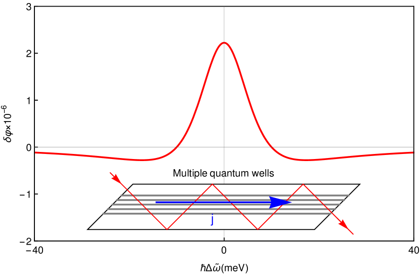
The dependence of on radiation frequency is shown in Fig. 3. Phase shift induced by CDOP exhibits maximum exactly at intersubband resonance position , it changes sign at and decays to zero away from resonance.
To increase the phase shift the sample with multiple quantum wells in wave-guide geometry can be used (see the inset in Fig. 3). For quantum wells and reflections phase shift caused by CDOP is . Modern technology allows to grow structure with both and , which yields the induced by CDOP phase shift , which can be reasonably well observed in the experiment.
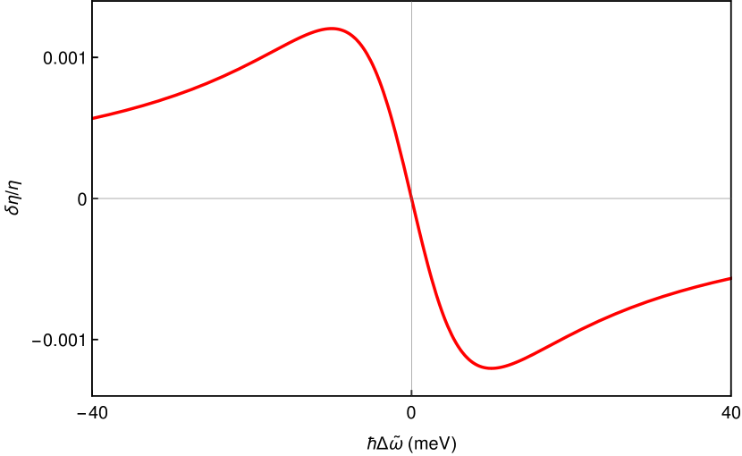
Another quantity which can be experimentally observed is absorbance. Relative correction to the absorbance induced by CDOP is given by
| (24) |
The dependence of is shown in Fig. 4, the main features of relative correction to the absorbance are as well observed at and . However, unlike the phase shift caused by CDOP is zero at intersubband resonance and has maximum at detuning . The characteristic value of of % is within reach of modern experimental capabilities.
Finally we point out that shift of resonance position is actually exactly matches the Doppler shift in the frame of reference moving with , which further supports the title of “current drag of photons”.
V Summary
Microscopic theory of the drag of photons by electric current in quantum wells have been developed. It has been shown that absorbance, transmission, and reflection coefficients are affected by dc electric current in quantum well. We demonstrated that the CDOP is due to the asymmetry of intersubband transitions, this asymmetry appears by taking into account the shift of electron distribution in momentum space with respect to the wave vector of light. The main feature of the CDOP is the shift of intersubband resonance position by the value of . The corrections caused by CDOP to the phase shift and radiation absorption are estimated for GaAs based quantum wells.
VI Acknowledgments
This work has been supported by the RFBR, project number 19-02-00273. G.V.B. also acknowledges support by the Foundation for the Advancement of Theoretical Physics and Mathematics “BASIS”.
References
- Ivchenko and Pikus (1997) E. L. Ivchenko and G. E. Pikus, Superlattices and Other Heterostructures (Springer Berlin Heidelberg, 1997), URL https://doi.org/10.1007/978-3-642-60650-2.
- Vorob’ev et al. (1979) L. E. Vorob’ev, E. L. Ivchenko, G. Pikus, I. Farbshtein, V. Shalygin, and A. Shturbin, JETP LETTERS 29, 441 (1979), ISSN 0021-3640.
- Tate et al. (2015) N. Tate, T. Kawazoe, W. Nomura, and M. Ohtsu, Scientific Reports 5 (2015), URL https://doi.org/10.1038/srep12762.
- Lee et al. (1967) C. H. Lee, R. K. Chang, and N. Bloembergen, Phys. Rev. Lett. 18, 167 (1967), URL https://link.aps.org/doi/10.1103/PhysRevLett.18.167.
- Khurgin (1995) J. B. Khurgin, Applied Physics Letters 67, 1113 (1995), URL https://doi.org/10.1063/1.114978.
- Ruzicka et al. (2012) B. A. Ruzicka, L. K. Werake, G. Xu, J. B. Khurgin, E. Y. Sherman, J. Z. Wu, and H. Zhao, Phys. Rev. Lett. 108, 077403 (2012), URL https://link.aps.org/doi/10.1103/PhysRevLett.108.077403.
- An et al. (2014) Y. Q. An, J. E. Rowe, D. B. Dougherty, J. U. Lee, and A. C. Diebold, Phys. Rev. B 89, 115310 (2014), URL https://link.aps.org/doi/10.1103/PhysRevB.89.115310.
- Gibson et al. (1970) A. F. Gibson, M. F. Kimmitt, and A. C. Walker, Applied Physics Letters 17, 75 (1970), URL https://doi.org/10.1063/1.1653315.
- Danishevskii et al. (1970) A. M. Danishevskii, A. A. Kastal’skii, S. M. Ryvkin, and I. D. Yaroshetskii, Sov. Phys. JETP 31, 292 (1970).
- Ganichev and Prettl (2005) S. Ganichev and W. Prettl, Intense Terahertz Excitation of Semiconductors (Oxford University Press (OUP), 2005), URL http://www.oxfordscholarship.com/view/10.1093/acprof:oso/9780198528302.001.0001/acprof-9780198528302.
- Shalygin et al. (2017) V. A. Shalygin, M. D. Moldavskaya, S. N. Danilov, I. I. Farbshtein, and L. E. Golub, Journal of Physics: Conference Series 864, 012072 (2017), URL https://doi.org/10.1088/1742-6596/864/1/012072.
- Luryi (1987) S. Luryi, Phys. Rev. Lett. 58, 2263 (1987), URL https://link.aps.org/doi/10.1103/PhysRevLett.58.2263.
- A. Grinberg and Luryi (1988) A. A. Grinberg and S. Luryi, Phys. Rev. B 38, 87 (1988), URL http://link.aps.org/doi/10.1103/PhysRevB.38.87.
- Ganichev et al. (2002) S. Ganichev, E. Ivchenko, and W. Prettl, Physica E: Low-dimensional Systems and Nanostructures 14, 166 (2002), URL https://doi.org/10.1016/s1386-9477(02)00371-5.
- Shalygin et al. (2007) V. A. Shalygin, H. Diehl, C. Hoffmann, S. N. Danilov, T. Herrle, S. A. Tarasenko, D. Schuh, C. Gerl, W. Wegscheider, W. Prettl, et al., JETP Letters 84, 570 (2007), URL https://doi.org/10.1134/s0021364006220097.
- Stachel et al. (2014) S. Stachel, G. V. Budkin, U. Hagner, V. V. Bel’kov, M. M. Glazov, S. A. Tarasenko, S. K. Clowes, T. Ashley, A. M. Gilbertson, and S. D. Ganichev, Phys. Rev. B 89, 115435 (2014), URL https://link.aps.org/doi/10.1103/PhysRevB.89.115435.
- Rogalski (2010) A. Rogalski, Infrared Detectors (CRC, Boca Raton, FL, 2010).
- Vorob’ev et al. (2000) L. E. Vorob’ev, D. V. Donetskii, and D. A. Firsov, Journal of Experimental and Theoretical Physics Letters 71, 331 (2000), URL https://doi.org/10.1134/1.568344.
- Ando et al. (1982) T. Ando, A. B. Fowler, and F. Stern, Rev. Mod. Phys. 54, 437 (1982), URL https://link.aps.org/doi/10.1103/RevModPhys.54.437.
- Ivchenko (2005) E. Ivchenko, Optical Spectroscopy of Semiconductor Nanostructures (Alpha Science, 2005), ISBN 9781842651506, URL https://books.google.co.uk/books?id=6PkomIC2WqMC.
- Bloss (1989) W. L. Bloss, Journal of Applied Physics 66, 3639 (1989), URL https://doi.org/10.1063/1.344073.
- Schneider and Liu (2006) H. Schneider and H. C. Liu, Quantum Well Infrared Photodetectors (Springer Berlin Heidelberg, 2006), URL https://doi.org/10.1007/978-3-540-36324-8.
- Bandara et al. (1988) K. M. S. V. Bandara, D. D. Coon, B. O, Y. F. Lin, and M. H. Francombe, Applied Physics Letters 53, 1931 (1988), URL https://doi.org/10.1063/1.100327.
- Steed (2013) R. Steed, Transfer matrix theory for a type of uniaxial layers: from basic electromagnetism to quantum well intersubband transitions (2013), URL https://www.researchgate.net/publication/236491437.