N-polar GaN/AlN resonant tunneling diodes
Abstract
N-polar GaN/AlN resonant tunneling diodes are realized on single-crystal N-polar GaN bulk substrate by plasma-assisted molecular beam epitaxy growth. The room-temperature current-voltage characteristics reveal a negative differential conductance (NDC) region with a peak tunneling current of kA/cm2 at a forward bias of 8 V. Under reverse bias, the polarization-induced threshold voltage is measured at V. These resonant and threshold voltages are well explained with the polarization field which is opposite to that of the metal-polar counterpart, confirming the N-polarity of the RTDs. When the device is biased in the NDC-region, electronic oscillations are generated in the external circuit, attesting to the robustness of the resonant tunneling phenomenon. In contrast to metal-polar RTDs, N-polar structures have the emitter on the top of the resonant tunneling cavity. As a consequence, this device architecture opens up the possibility of seamlessly interfacing—via resonant tunneling injection—a wide range of exotic materials with III-nitride semiconductors, providing a route to explore new device physics.
Resonant tunneling transport in III-nitride heterostructures has been under scrutiny over the last two decades Kikuchi, Bannai, and Kishino (2001); Kikuchi et al. (2002); Golka et al. (2006); Bayram, Vashaei, and Razeghi (2010); Sakr et al. (2012); Li et al. (2012); Grier et al. (2015). However, only during the last four years robust quantum interference effects and room temperature negative differential conductance were reported in nitride-based double-barrier heterostructures Encomendero et al. (2016); Growden et al. (2016); Encomendero et al. (2017, 2018, 2019); Wang et al. (2019); Encomendero et al. (2020); Encomendero, Jena, and Xing (2020). Over this period, multiple advances in epitaxial growth, polar heterostructure design, device fabrication techniques, and tunneling transport theory, have been instrumental in advancing our understanding of resonant tunneling injection across polar semiconductors, leading to the realization of high-performance III-nitride resonant tunneling diodes (RTDs).
The technological importance of nitride-based resonant tunneling injection stems from the possibility of engineering the electron transport dynamics, thereby enabling the operation of ultra-high-speed electronic devices.Izumi, Suzuki, and Asada (2017); Kanaya et al. (2014, 2015) Owing to their high breakdown electric field, high longitudinal optical phonon energy, and high thermal conductivity, nitride semiconductors represent a promising platform for the development of high-speed and high-power electronic and photonic devices.Cho et al. (2017, 2019) In spite of their outstanding material properties, III-nitride semiconductors exhibit strong internal polarization fields which makes the engineering of quantum confined states, a nontrivial task.
Due to their noncentrosymmetric crystal structure, nitride heterostructures grown along the polar -axis, result in a discontinuous electrical polarization which gives rise to highly localized polarization charges . Here, is the polarization discontinuity at the heterojunction interface, is the absolute value of the electron charge, and is the unitary vector along the growth direction. The presence of these sheets of polarization charge in turn generates strong internal spontaneous and piezoelectric polarization fields with magnitudes on the order of 1–10 MV/cm ( is the dielectric constant).Bernardini, Fiorentini, and Vanderbilt (1997) Due to their strength, they modulate the spacial distribution of free carriers, determine the strength and direction of internal electric fields, and dominate the energy band profile of nitride heterostructures. This distinctive feature greatly broadens the design space of polar heterostructures via polarization engineering.Jena et al. (2011) This technique has been exploited in various photonic and electronic devices to induce 2DKhan et al. (1992); Chaudhuri et al. (2019) and 3DJena et al. (2002); Simon et al. (2010) free carrier populations, couple electron and hole states via interband tunneling,Simon et al. (2009); Krishnamoorthy et al. (2013); Yan et al. (2015) and demonstrate a wide bandgap tunneling field-effect transistor.Chaney et al. (2020)
In III-nitride resonant tunneling heterostructures, the physics of resonant injection is greatly influenced by the interfacial polarization charges present at every heterojunction. Under equilibrium conditions, the interplay between the fixed polarization charges and mobile free carriers leads to a redistribution of electrons around the active region. This effect results in the accumulation of free electrons around the positive polarization charges , on one side of the active structure. On the opposite side, the negative sign of the polarization charge (i.e. ) repels free carriers, inducing a depletion layer that effectively widens the adjacent tunneling barrier. Therefore, whereas electrons on the emitter 2D electron gas (2DEG) can readily tunnel into the active region, carriers on the collector region undergo a strong attenuation by the wide depletion layer.Encomendero et al. (2019, 2020) This analysis reveals that, in polar RTDs, the position of the emitter electrode, with respect to the double-barrier structure, is determined by the polarity of the crystal, which controls the sign of the polarization discontinuity .
Metal-polar RTDs—grown along the [0001] direction—have the emitter buried below the double-barrier structure, thereby limiting its electrostatic control by means of surface metallic electrodes. In contrast, by flipping the polarity of the crystal, we can re-locate the emitter on the top of the resonant tunneling heterostructure. This device architecture allows un-screened control over the 2DEG population via field-effect, benefiting not only vertical but also lateral transport. This advantage has been recently exploited for the manufacture of highly-scaled enhancement-mode transistors with outstanding power capabilities.Singisetti, Wong, and Mishra (2013); Wong et al. (2013); Wong and Mishra (2019) Using this architecture, highly-scaled transistors with 2DEG channels located at nm from the top surface, have been manufactured, attesting to the excellent electrostatic control over the 2DEG.Singisetti et al. (2012) In addition, N-polar high electron mobility transistors (HEMTs), could be potentially readily integrated with a resonant tunneling cavity, enabling electronic gain within the terahertz band.Sensale-Rodriguez et al. (2013); Zhao et al. (2014); Condori Quispe et al. (2016) N-polar-based polarization engineering is also promising for the design III-nitride photocathodesMarini et al. (2018), light-emitting diodesSimon et al. (2010); Verma et al. (2011); Bharadwaj et al. (2020); Turski et al. (2019) and solar cellsLi et al. (2011) with enhanced emission, injection, and collection efficiencies, respectively. More fundamentally, epitaxy along the [000] direction offers additional advantages stemming from the higher thermal stability of the N-polar crystal surface.VanMil et al. (2004); Togashi et al. (2009); Okumura et al. (2014); Xu and Yoshikawa (2003)
In the case of III-nitride resonant tunneling devices, the N-polar platform allows not only an enhanced control over the source of tunneling carriers, but can also enable monolithic integration of the double-barrier structure with a variety of functional materials at the top emitter contact. From the crystal growth point of view, this is a significant advantage because highly dissimilar materials such as ferromagnets and superconductors can replace the semiconductor emitter, without compromising the structural quality of the double-barrier structure underneath. This device architecture opens up the possibility of seamlessly interfacing—via resonant tunneling injection—a wide range of exotic materials with III-nitride semiconductors, providing a route to explore new device physics.Jena et al. (2019)
In spite of their multiple advantages, N-polar resonant tunneling heterostructures have not been demonstrated so far mainly due to the lack of high-quality substrates, coupled with the difficulty of growing tunneling heterostructures on crystals containing a high density of dislocations. By virtue of advanced nitride growth technology, however, high-quality N-polar GaN substrates with low dislocation densities have recently become commercially available.
In this paper, by taking advantage of single-crystal GaN substrates, we report the molecular-beam-epitaxy (MBE) growth, fabrication, and tunneling transport characteristics of N-polar RTDs, exhibiting robust negative differential conductance (NDC) and RF oscillations at room temperature.
GaN/AlN double-barrier heterostructures were grown on single-crystal N-polar GaN wafers—with a dislocation density of cm-2 using a Veeco GENxplor MBE system equipped with standard effusion cells for elemental Ga, Al and Si, and a radio-frequency plasma source for the active N species. The base pressure of the growth chamber was in the range of 10-10 Torr under idle conditions, and Torr during growth. The device structure consists of the following layers, starting from the nucleation surface: 100 nm GaN:Si / 6 nm GaN / 2.2 nm AlN / 3 nm GaN / 2.2 nm AlN / 10 nm GaN / 100 nm GaN:Si, as shown in Fig. 1(a). The GaN and GaN:Si layers are grown under Ga-rich conditions (7.8 nm-2 s-1; 4.1 nm-2 s-1) and the AlN barriers are grown at nominally stoichiometric condition (i.e., 4.1 nm-2 s-1), under the Ga flux (7.8 nm-2 s-1), to ensure a metal-rich condition (); where , and are Ga, Al and active N fluxes, respectively. The entire heterostructure was grown at a constant substrate thermocouple temperature of 700 ∘C. The excess Ga droplets after the growth were removed in HCl before ex situ characterization and device fabrication.
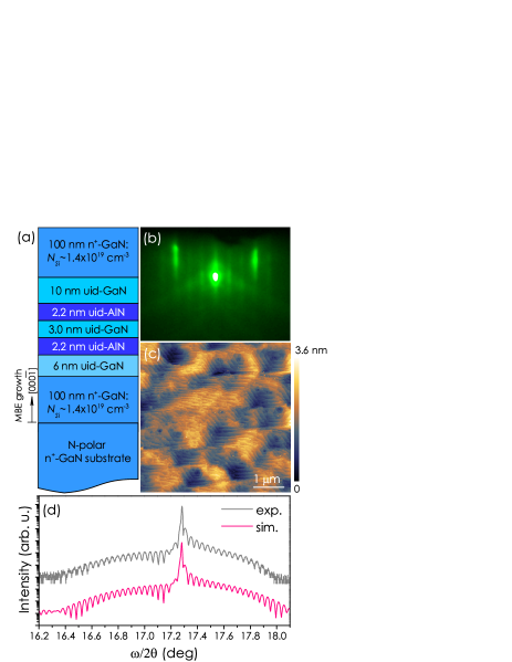
Figure 1(b) displays the reflection high-energy electron diffraction (RHEED) pattern of the RTD sample taken at low temperature ( ∘C) after growth. It reveals pure reflection patterns with a well-defined specular spot and pronounced Kikuchi lines, indicating smooth surface morphology and high structural order. More importantly, a surface reconstruction is clearly observed, confirming that the N-polarity has been preserved up to the top layer. Atomic force microscopy (AFM) reveals a smooth surface morphology exhibiting clear atomic steps [see Fig. 1(c)]. In addition, Fig. 1(d) shows the symmetric x-ray diffraction (XRD) scan of the double-barrier structure. Excellent agreement between the simulated curve, based on the layer structure in Fig. 1(a), and the experimental data is obtained. This result indicates that the GaN/AlN interfaces exhibit atomically abrupt transitions, which is critical for coherent electron injection.
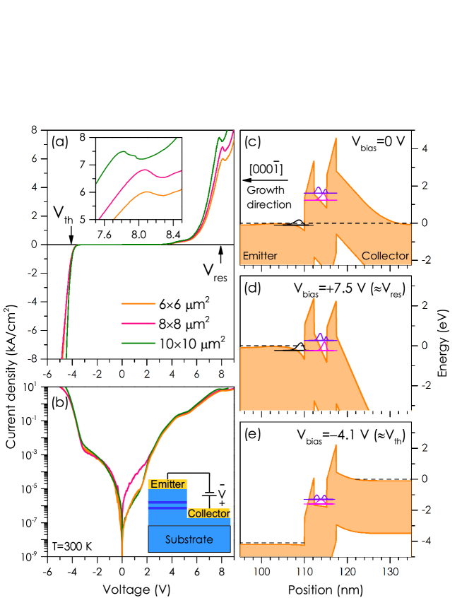
After growth, RTDs are fabricated by conventional contact lithography, reactive ion etching and electron-beam metal evaporation for ohmic contacts. Figures 2(a) and 2(b) display the room-temperature current-voltage (J-V) characteristics of three devices with different mesa areas, plotted in linear and logarithmic scales, respectively. The test circuit, shown schematically in the inset of Fig. 2(b), is set up such that the forward bias direction corresponds to electronic flow from the top emitter, through the double-barrier, into the collector contact at the bottom of the active region. These J-V curves clearly resemble the electronic transport characteristics of metal-polar GaN/AlN RTDs, but with a flipped voltage bias polarity.Encomendero et al. (2017, 2019, 2020)
As discussed previously, the sheets of charge , located at the GaN/AlN interfaces, induce a rearrangement of free carriers. Owing to the lack of inversion symmetry in the spatial distribution of these polarization charges, the internal electric fields inside the GaN quantum well and AlN barriers exhibit antiparallel orientations. This can be seen in the equilibrium energy band diagram of Fig. 2(c), calculated by solving Schrödinger and Poisson equations self-consistently. More importantly, the broken symmetry in the charge distribution results in the polarization-induced broadening of the collector tunneling barrier, which strongly attenuates electron tunneling transmission. As a consequence, under low current injection (i.e. V), electronic transport is supported mainly by thermally activated carriers.Encomendero et al. (2017, 2020) However, as the forward bias increases (i.e. V), the collector tunneling transmission grows exponentially, thereby restoring the symmetry between the emitter and collector transmission coefficients. As a consequence, constructive quantum interference within the well leads to an enhanced resonant tunneling transmission.Encomendero et al. (2019) When V, the emitter Fermi level gets aligned with the ground state of the well, enabling resonant tunneling injection across the active region. The detuning from this resonant condition results in the conductance modulation observed between 4 and 5 V [see Figs. 2(a) and (b)]. The main resonant peak occurs at V, with a peak resonant tunneling current kA/cm2, measured in multiple devices across the 7 mm7 mm RTD sample [see the inset of Fig. 2(a)]. This result is consistent with the resonant tunneling alignment between the emitter subband and the ground state within the well, as can be seen from the band diagram shown in Fig. 2(d). When the forward bias increases above the resonant tunneling voltage, the diodes exhibit a region of NDC that extends approximately over 0.2 V, resulting in a peak-to-valley-current ratio (PVCR) of at room temperature [see the inset of Fig. 2(a)]. The origin of the low PVCR is attributed to the presence of leakage mechanisms across the double-barrier active region, resulting in a larger valley current and thereby degrading this important RTD metric. However as pointed out previously, the presence of these leakage paths do not prevent resonant tunneling transport within the N-polar double-barrier structure. Minimizing the magnitude of the non-resonant leakage current will require further optimization in the RTD growth conditions.
Whereas forward bias injection leads to an enhanced resonant tunneling transmission, the opposite bias polarity results in an increasingly high asymmetry between the tunneling barriers.Encomendero et al. (2017, 2019) Within this bias regime, a critical condition is achieved when electronic injection transitions from double-barrier resonant tunneling transport to single-barrier tunneling injection. This critical condition can be seen in Fig. 2(e) and occurs when polar RTDs are biased at the threshold voltage , where is the thickness of the tunneling barriers.Encomendero et al. (2017) From Fig. 2(a), we measure the characteristic threshold voltage V, using the method described in Ref. Encomendero et al., 2019. Employing the barrier thickness nm, measured from the XRD pattern, we obtain the magnitude of the internal polarization fields along the -direction to be MV/cm. This experimental result is in reasonable agreement with previous theoretical calculations.Bernardini, Fiorentini, and Vanderbilt (1997)
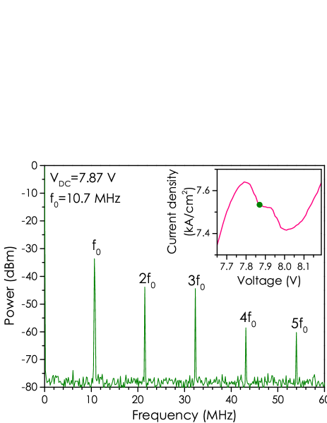
To conclusively demonstrate the robustness of the resonant tunneling phenomena in our devices, we construct an oscillator circuit that exploits the room temperature NDC of the RTDs as the gain mechanism. It should be noted that the critical condition for the generation of high-speed electronic oscillations is that , where is the RTD conductance; , , and are the series resistance, capacitance, and inductance of the biasing circuit, external to double-barrier structure Hines (1960). Since the absolute value of is proportional to the mesa area of the device, RTDs with larger areas and thereby higher current levels are employed for the assembly of the oscillator. The transition through the critical oscillation condition can be seen in the inset of Fig. 2(a). The device, featuring the largest mesa area, generates oscillations in the external measurement circuit, which manifests in the chair-like shape within the NDC region. In contrast, the smaller area devices in the same figure, do not present the chair-like feature which indicates that no ac oscillations are generated. This condition can be met either by scaling the RTD area or by biasing-circuit stabilization techniques published elsewhere Sollner et al. (1984); Shewchuk et al. (1985); Cornescu et al. (2019).
The oscillator consists of a single N-polar RTD, with an area of m2, connected to a dc voltage source and spectrum analyzer via a bias tee. When the diode is biased within the region of the NDC—shown in the inset of Fig. 3— self-oscillations build-up in the external circuit. Figure 3 shows the power spectrum generated by resonant tunneling oscillator when the device is biased at V. Owing to the non-linear characteristics of the differential conductance, the output spectrum contains not only the fundamental frequency , but also multiple harmonics up to the fifth overtone.Sollner et al. (1988); Asada (2001) The output power and frequency of the fundamental component, measured at 0.43 W and 10.7 MHz respectively, are determined by the external biasing circuit instead of the intrinsic frequency response of the RTD.Encomendero et al. (2018) Additionally, we would like to highlight that the generation of continuous and stable electronic oscillations from our devices confirm the repeatable behavior of the NDC. Therefore, under operation, the N-polar RTD-oscillator generates an ac signal which scans the NDC region at a rate of approximately sweeps per second, conclusively confirming the repeatability of the resonant tunneling phenomenon.
In summary, we experimentally demonstrated that resonant tunneling transport can be engineered in GaN/AlN double-barrier heterostructures grown along the [000] direction. Electronic transport at room temperature, reveals a peak resonant tunneling current kA/cm2 and a resonant bias V. When the devices are biased within the NDC region, electronic oscillations are generated in the external circuit, attesting to the robustness of the resonant tunneling phenomenon. These results constitute the conclusive demonstration of room-temperature resonant tunneling injection in N-polar RTDs capable of ac power generation. Finally, it should be noted that in contrast to metal-polar RTDs, N-polar structures have the emitter on the top of the resonant tunneling cavity. As a consequence, this device architecture opens up the possibility of seamlessly interfacing—via resonant tunneling injection—a wide range of exotic materials with III-nitride semiconductors, providing a route to explore new device physics.
The authors thank Zexuan Zhang for useful discussion. This work was supported in part by the AFOSR (No. FA9550-17-1-0048), NSF DMREF (No. 1534303), NSF RAISE TAQs (No. 1839196), the Semiconductor Research Corporation (SRC) Joint University Microelectronics Program (JUMP), NSF NewLaw (No. EFMA-1741694), and ONR (Nos. N00014-20-1-2176 and N00014-17-1-2414). This work made use of the shared facilities that are supported through the NSF ECCS-1542081, NSF DMR-1719875, and NSF DMR-1338010.
References
- Kikuchi, Bannai, and Kishino (2001) A. Kikuchi, R. Bannai, and K. Kishino, Phys. Status Solidi A 188, 187–190 (2001).
- Kikuchi et al. (2002) A. Kikuchi, R. Bannai, K. Kishino, C.-M. Lee, and J.-I. Chyi, Appl. Phys. Lett. 81, 1729 (2002).
- Golka et al. (2006) S. Golka, C. Pflügl, W. Schrenk, G. Strasser, C. Skierbiszewski, M. Siekacz, I. Grzegory, and S. Porowski, Appl. Phys. Lett. 88, 172106 (2006).
- Bayram, Vashaei, and Razeghi (2010) C. Bayram, Z. Vashaei, and M. Razeghi, Appl. Phys. Lett. 96, 042103 (2010).
- Sakr et al. (2012) S. Sakr, Y. Kotsar, M. Tchernycheva, E. Warde, N. Isac, E. Monroy, and F. H. Julien, Appl. Phys. Express 5, 052203 (2012).
- Li et al. (2012) D. Li, L. Tang, C. Edmunds, J. Shao, G. Gardner, M. J. Manfra, and O. Malis, Appl. Phys. Lett. 100, 252105 (2012).
- Grier et al. (2015) A. Grier, A. Valavanis, C. Edmunds, J. Shao, J. Cooper, G. Gardner, M. Manfra, O. Malis, D. Indjin, Z. Ikonić, et al., J. Appl. Phys. 118, 224308 (2015).
- Encomendero et al. (2016) J. Encomendero, F. A. Faria, S. Islam, V. Protasenko, S. Rouvimov, P. Fay, D. Jena, and H. G. Xing, arXiv preprint arXiv:1606.08100 (2016).
- Growden et al. (2016) T. A. Growden, D. F. Storm, W. Zhang, E. R. Brown, D. J. Meyer, P. Fakhimi, and P. R. Berger, Appl. Phys. Lett. 109, 083504 (2016).
- Encomendero et al. (2017) J. Encomendero, F. A. Faria, S. Islam, V. Protasenko, S. Rouvimov, B. Sensale-Rodriguez, P. Fay, D. Jena, and H. G. Xing, Phys. Rev. X 7, 041017 (2017).
- Encomendero et al. (2018) J. Encomendero, R. Yan, A. Verma, S. Islam, V. Protasenko, S. Rouvimov, P. Fay, D. Jena, and H. G. Xing, Appl. Phys. Lett. 112, 103101 (2018).
- Encomendero et al. (2019) J. Encomendero, V. Protasenko, B. Sensale-Rodriguez, P. Fay, F. Rana, D. Jena, and H. G. Xing, Phys. Rev. Appl. 11, 034032 (2019).
- Wang et al. (2019) D. Wang, J. Su, Z. Chen, T. Wang, L. Yang, B. Sheng, S. Lin, X. Rong, P. Wang, X. Shi, et al., Adv. Electron. Mater. 5, 1800651 (2019).
- Encomendero et al. (2020) J. Encomendero, V. Protasenko, F. Rana, D. Jena, and H. G. Xing, Phys. Rev. Appl. 13, 034048 (2020).
- Encomendero, Jena, and Xing (2020) J. Encomendero, D. Jena, and H. G. Xing, “Resonant Tunneling Transport in Polar III-Nitride Heterostructures,” in High-Frequency GaN Electronic Devices (Springer International Publishing, Cham, 2020) pp. 215–247.
- Izumi, Suzuki, and Asada (2017) R. Izumi, S. Suzuki, and M. Asada, in 2017 42nd International Conference on Infrared, Millimeter, and Terahertz Waves (IRMMW-THz) (IEEE, 2017) pp. 1–2.
- Kanaya et al. (2014) H. Kanaya, R. Sogabe, T. Maekawa, S. Suzuki, and M. Asada, J. Infrared Millim. Terahertz Waves 35, 425 (2014).
- Kanaya et al. (2015) H. Kanaya, T. Maekawa, S. Suzuki, and M. Asada, Jpn. J. Appl. Phys. 54, 094103 (2015).
- Cho et al. (2017) Y.-J. Cho, Z. Hu, K. Nomoto, H. G. Xing, and D. Jena, Appl. Phys. Lett. 110, 253506 (2017).
- Cho et al. (2019) Y.-J. Cho, S. Bharadwaj, Z. Hu, K. Nomoto, U. Jahn, H. G. Xing, and D. Jena, Jpn. J. Appl. Phys. 58, 060914 (2019).
- Bernardini, Fiorentini, and Vanderbilt (1997) F. Bernardini, V. Fiorentini, and D. Vanderbilt, Phys. Rev. B 56, R10024 (1997).
- Jena et al. (2011) D. Jena, J. Simon, A. Wang, Y. Cao, K. Goodman, J. Verma, S. Ganguly, G. Li, K. Karda, V. Protasenko, et al., Phys. Status Solidi A 208, 1511 (2011).
- Khan et al. (1992) M. A. Khan, J. N. Kuznia, J. M. Van Hove, N. Pan, and J. Carter, Appl. Phys. Lett. 60, 3027 (1992).
- Chaudhuri et al. (2019) R. Chaudhuri, S. J. Bader, Z. Chen, D. A. Muller, H. G. Xing, and D. Jena, Science 365, 1454 (2019).
- Jena et al. (2002) D. Jena, S. Heikman, D. Green, D. Buttari, R. Coffie, H. Xing, S. Keller, S. DenBaars, J. S. Speck, U. K. Mishra, and et al., Appl. Phys. Lett. 81, 4395 (2002).
- Simon et al. (2010) J. Simon, V. Protasenko, C. Lian, H. Xing, and D. Jena, Science 327, 60 (2010).
- Simon et al. (2009) J. Simon, Z. Zhang, K. Goodman, H. Xing, T. Kosel, P. Fay, and D. Jena, Phys. Rev. Lett. 103, 026801 (2009).
- Krishnamoorthy et al. (2013) S. Krishnamoorthy, F. Akyol, P. S. Park, and S. Rajan, Appl. Phys. Lett. 102, 113503 (2013).
- Yan et al. (2015) X. Yan, W. Li, S. M. Islam, K. Pourang, H. Xing, P. Fay, and D. Jena, Appl. Phys. Lett. 107, 163504 (2015).
- Chaney et al. (2020) A. Chaney, H. Turski, K. Nomoto, Z. Hu, J. Encomendero, S. Rouvimov, T. Orlova, P. Fay, A. Seabaugh, H. G. Xing, et al., Appl. Phys. Lett. 116, 073502 (2020).
- Singisetti, Wong, and Mishra (2013) U. Singisetti, M. H. Wong, and U. K. Mishra, Semicond. Sci. Technol. 28, 074006 (2013).
- Wong et al. (2013) M. H. Wong, S. Keller, S. D. Nidhi, D. J. Denninghoff, S. Kolluri, D. F. Brown, J. Lu, N. A. Fichtenbaum, E. Ahmadi, U. Singisetti, et al., Semicond. Sci. Technol. 28, 074009 (2013).
- Wong and Mishra (2019) M. H. Wong and U. K. Mishra, “N-polar III-nitride Transistors,” in Semiconductors and Semimetals, Vol. 102 (Elsevier, 2019) p. 329–395.
- Singisetti et al. (2012) U. Singisetti, M. H. Wong, J. S. Speck, and U. K. Mishra, IEEE Electron Device Lett. 33, 26–28 (2012).
- Sensale-Rodriguez et al. (2013) B. Sensale-Rodriguez, L. Liu, P. Fay, D. Jena, and H. G. Xing, IEEE Trans. Terahertz Sci. Technol. 3, 200 (2013).
- Zhao et al. (2014) Y. Zhao, W. Chen, W. Li, M. Zhu, Y. Yue, B. Song, J. Encomendero, B. Sensale-Rodriguez, H. Xing, and P. Fay, Appl. Phys. Lett. 105, 173508 (2014).
- Condori Quispe et al. (2016) H. O. Condori Quispe, J. J. Encomendero-Risco, H. G. Xing, and B. Sensale-Rodriguez, Appl. Phys. Lett. 109, 063111 (2016).
- Marini et al. (2018) J. Marini, I. Mahaboob, E. Rocco, L. D. Bell, and F. Shahedipour-Sandvik, J. Appl. Phys. 124, 113101 (2018).
- Verma et al. (2011) J. Verma, J. Simon, V. Protasenko, T. Kosel, H. Grace Xing, and D. Jena, Appl. Phys. Lett. 99, 171104 (2011).
- Bharadwaj et al. (2020) S. Bharadwaj, J. Miller, K. Lee, J. Lederman, M. Siekacz, H. G. Xing, D. Jena, C. Skierbiszewski, and H. Turski, Opt. Express 28, 4489 (2020).
- Turski et al. (2019) H. Turski, S. Bharadwaj, H. Xing, and D. Jena, J. Appl. Phys. 125, 203104 (2019).
- Li et al. (2011) Z. Li, M. Lestradet, Y. Xiao, and S. Li, Phys. Status Solidi A 208, 928 (2011).
- VanMil et al. (2004) B. L. VanMil, H. Guo, L. J. Holbert, K. Lee, T. H. Myers, T. Liu, and D. Korakakis, J. Vac. Sci. Technol. B 22, 2149 (2004).
- Togashi et al. (2009) R. Togashi, T. Kamoshita, H. Adachi, H. Murakami, Y. Kumagai, and A. Koukitu, Phys. Status Solidi C 6, S372 (2009).
- Okumura et al. (2014) H. Okumura, B. M. McSkimming, T. Huault, C. Chaix, and J. S. Speck, Appl. Phys. Lett. 104, 012111 (2014).
- Xu and Yoshikawa (2003) K. Xu and A. Yoshikawa, Appl. Phys. Lett. 83, 251 (2003).
- Jena et al. (2019) D. Jena, R. Page, J. Casamento, P. Dang, J. Singhal, Z. Zhang, J. Wright, G. Khalsa, Y. Cho, and H. G. Xing, Jpn. J. Appl. Phys. 58, SC0801 (2019).
- Hines (1960) M. E. Hines, Bell Syst. Tech. J. 39, 477–513 (1960).
- Sollner et al. (1984) T. C. L. G. Sollner, P. E. Tannenwald, D. D. Peck, and W. D. Goodhue, Appl. Phys. Lett. 45, 1319 (1984).
- Shewchuk et al. (1985) T. J. Shewchuk, J. M. Gering, P. C. Chapin, P. D. Coleman, W. Kopp, C. K. Peng, and H. Morkoç, Appl. Phys. Lett. 47, 986 (1985).
- Cornescu et al. (2019) A. C. Cornescu, R. Morariu, A. Ofiare, A. Al-Khalidi, J. Wang, J. M. L. Figueiredo, and E. Wasige, IEEE Trans. Microw. Theory Tech. 67, 3449–3454 (2019).
- Sollner et al. (1988) T. C. Sollner, E. R. Brown, W. D. Goodhue, and C. A. Correa, J. Appl. Phys. 64, 4248 (1988).
- Asada (2001) M. Asada, Jpn. J. Appl. Phys. 40, 6809 (2001).