WoLFRaM: Enhancing Wear-Leveling and Fault Tolerance
in Resistive Memories using Programmable Address Decoders
Abstract
Resistive memories have limited lifetime caused by limited write endurance and highly non-uniform write access patterns. Two main techniques to mitigate endurance-related memory failures are 1) wear-leveling, to evenly distribute the writes across the entire memory, and 2) fault tolerance, to correct memory cell failures. However, one of the main open challenges in extending the lifetime of existing resistive memories is to make both techniques work together seamlessly and efficiently.
To address this challenge, we propose WoLFRaM, a new mechanism that combines both wear-leveling and fault tolerance techniques at low cost by using a programmable resistive address decoder (PRAD). The key idea of WoLFRaM is to use PRAD for implementing 1) a new efficient wear-leveling mechanism that remaps write accesses to random physical locations on the fly, and 2) a new efficient fault tolerance mechanism that recovers from faults by remapping failed memory blocks to available physical locations. Our evaluations show that, for a Phase Change Memory (PCM) based system with cell endurance of writes, WoLFRaM increases the memory lifetime by 68% compared to a baseline that implements the best state-of-the-art wear-leveling and fault correction mechanisms. WoLFRaM’s average / worst-case performance and energy overheads are 0.51% / 3.8% and 0.47% / 2.1% respectively.
1 Introduction
Resistive memories provide significant advantages over DRAM in terms of non-volatility and technology scaling [49, 84, 109, 85, 115, 50, 72, 51, 121]. However, the limited write endurance of resistive memories, e.g., - writes per memory cell in Phase Change Memory (PCM) [29, 122, 50, 52], limits their usage as main memory. Workloads with significant non-uniformity in write access patterns can cause early failures in rows that are heavily written, which decreases the expected memory lifetime [82, 83, 50]. To increase lifetime, resistive memories implement wear-leveling techniques [121, 41, 95, 82, 88, 83, 116, 117, 25, 29, 122, 120, 22, 21, 62, 61, 77, 2, 34, 23] for leveling out the write non-uniformity by remapping frequent writes to less heavily written locations. Unfortunately, memory cells can have very different write endurance levels due to process variation, which makes wear-leveling more challenging.
Existing wear-leveling techniques have four drawbacks. First, many early proposals do not consider the write patterns of applications when remapping write accesses. As a result, some applications may wear memory out much more quickly than others. Second, some techniques do not consider endurance variation across different memory cells [82, 88, 121], which can cause early memory failures due to the failure of cells with lower write endurance. Third, some existing mechanisms [2, 61, 122] remap writes at a coarse granularity (e.g., at the granularity of pages or even larger memory regions), which reduces wear-leveling efficiency. Fourth, most techniques are relatively slow because they level out the write non-uniformity in a sequential fashion. The goal of wear-leveling is to extend the lifetime of memory cells as much as possible. Once memory cells reach their endurance limits, resistive memory needs fault tolerance to continue operating. Fault tolerance mechanisms [87, 89, 26, 81, 113, 5, 69, 103, 13, 12, 66, 16, 15, 67, 9, 14, 11, 10, 17, 35, 4, 7, 8, 47, 48, 57, 58, 60, 64, 65, 76, 102] typically enable recovery from several failed bits per data page or data block.
Unfortunately, to our knowledge, there is no technique that combines both wear-leveling and fault tolerance techniques in a seamless way to 1) level out the write non-uniformity and 2) tolerate faults when memory cells reach their endurance limits. A previous work [25] shows that naively combining both techniques can result into the malfunction of the system: a commonly-used wear-leveling technique stops working seamlessly once the first data block fails and is mapped out, since the data block’s physical position becomes unavailable as a remapping target [25].
Our goal in this paper is to 1) mitigate the shortcomings of existing wear-leveling mechanisms, and 2) enable seamless and efficient integration of wear-leveling and fault tolerance techniques. To this end, we propose WoLFRaM (Wear-Leveling and Fault tolerance for Resistive Memories), the first integrated mechanism that combines both wear-leveling and fault tolerance. The overarching key idea of WoLFRaM is to use a Programmable Resistive Address Decoder (PRAD) [110] to decouple memory addresses from physical memory locations, which serves as a remapping substrate that seamlessly enables both wear-leveling and fault tolerance.
PRAD allows programming arbitrary addresses into an address decoder position (i.e., a decoder row), which enables dynamic assignment of addresses to physical memory rows. During a memory access, PRAD selects the decoder row (and consequently the memory row) where the address matches the stored pattern, similar to tag matching in associative caches. In contrast, conventional address decoders used in random access memories are hardwired, and the address of a memory row is permanently linked to the physical row of the decoder.
WoLFRaM wear-leveling mechanism periodically reprograms the address decoder to remap a write address to a different physical memory location. WoLFRaM implements a write-access-pattern-aware mechanism that remaps frequently-written addresses at a higher rate than infrequently-written addresses. WoLFRaM performs address remapping transparently, i.e., the data is accessed always with the same memory address while its physical location in the memory device might change. Compared to state-of-the-art wear-leveling mechanisms, WoLFRaM does not require external address remapping techniques, such as explicit remapping tables [117, 121], predictable arithmetic mapping [82, 88, 122], or page table reprogramming [2, 23, 77, 34, 61, 62, 119, 32, 31]. Compared to the commercially available Intel Optane DC Persistent Memory Module (Optane DC PMM) [36], WoLFRaM does not require a separate DRAM with power failure protection mechanisms for storing translation tables needed for wear-leveling.
WoLFRaM fault tolerance mechanism simply uses PRAD to remap the address of a failed memory row to an empty memory row without errors.
We evaluate our proposal using Phase Change Memory (PCM). Our results show that, compared to a state-of-the-art two-level Security Refresh wear-leveling mechanism [88] coupled with an failure correction mechanism [87], WoLFRaM achieves 1) 68% longer lifetime, 2) 0.51% (3.8%) average (maximum) performance overhead for SPEC CPU2006 benchmarks, and 3) 0.47% (2.1%) average (worst-case) energy overhead for SPEC CPU2006 benchmarks.
This paper makes the following key contributions:
-
•
We propose WoLFRaM, the first mechanism that seamlessly integrates wear-leveling and fault tolerance into resistive memories by using a Programmable Resistive Address Decoder (PRAD). WoLFRaM overcomes the four main drawbacks of previous mechanisms by 1) considering the write patterns of the application, 2) considering endurance variation across different memory cells, 3) remapping writes at fine granularity, and 4) performing wear-leveling 21.7x faster than the best state-of-the-art mechanism.
-
•
We evaluate the lifetime, performance and energy of WoLFRaM compared to a combination of a state-of-the-art wear-leveling mechanism [88] and a state-of-the-art fault tolerance mechanism [87]. Our results show that WoLFRaM provides a significantly longer memory lifetime at significantly lower performance and energy overheads.
2 Background
We provide the necessary background on the organization and operation of a typical resistive memory, and the basic operation of a conventional address decoder and a programmable resistive address decoder.
2.1 Resistive Memory Organization
A resistive memory contains multiple independently controlled banks [89, 50, 45, 71, 94], similar to DRAM. A resistive memory bank (Figure 1) is composed of an array of memory cells organized into multiple subarrays (e.g., 64-128 [45, 97, 71, 91, 19, 50, 51, 43, 20, 92, 90, 27, 94]) of multiple rows (e.g., 512-1024 [89, 45, 71, 91, 19, 50, 51, 43, 20, 92, 90, 27, 94]).
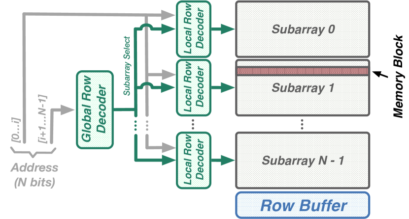
Bank-level address decoding is hierarchical. There are typically two address decoding levels [45]: 1) the global row decoder selects a subarray, and 2) the local row decoder selects a row in the subarray that contains the target memory block. The target memory block, typically 256B to 1kB [88, 45, 70, 71, 50, 18, 55, 53], is individually addressable within a subarray, while a subarray is individually addressable within a bank. Individual addressing is important since it enables fine-grained remapping of a single data block, as well as a single subarray.
2.2 Resistive Memory Operation
To serve a memory request that accesses data at a particular memory block, the memory controller issues three commands to a bank. Each command triggers a specific sequence of events within the bank. These commands [37, 38, 45, 55, 54, 56, 50, 70, 71, 97, 98], used commercially and in research [50, 45], are similar to the DDRx protocol commands:
-
•
ACT: an activate command, which reads the memory row into the row buffer.
- •
-
•
RD/WR: a read/write command, which reads/writes new data from/to the row buffer.
2.3 Conventional Address Decoder
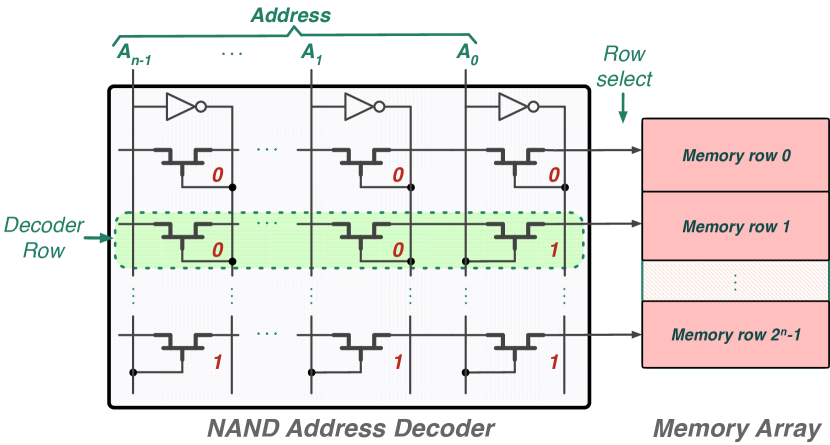
Figure 2 shows a conventional hardwired dynamic NAND address decoder that consists of an array of NMOS transistors. A conventional decoder selects a specific row of the memory array according to the input address. The mapping between the input address and the selected row in the memory array cannot be changed. The gates of the NMOS transistors in each decoder row are hardwired to either direct (e.g., ) or inverse address bitlines (e.g., ), according to the physical position of the decoder and memory rows. Additionally, a dynamic NAND address decoder typically includes precharge transistors, evaluation transistors, and a level keeper in each decoder row (not shown in Figure 2) [33].
2.4 Programmable Resistive Address Decoder
Our proposal relies on Programmable Resistive Address Decoders (PRADs) [110] to implement both wear-leveling and fault tolerance mechanisms for resistive memories.
Figure 3 shows a high-level overview of PRAD. PRAD decouples memory addresses from fixed physical locations within the memory array. PRAD provides a level of indirection that allows flexible and dynamic mapping of memory addresses onto arbitrary memory positions.
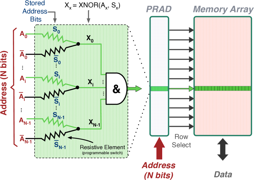
PRAD allows programming addresses into address decoder positions (i.e., decoder rows) using resistive elements. Each stored address bit in a decoder row can be programmed with two resistive elements (e.g., and in Figure 3). During memory access, the address is looked up in a fully-associative fashion: a pair of resistive elements functions as an XNOR gate that compares a bit of the input address (e.g., ) to the stored address bit (e.g., ). If and have the same value, the input is asserted in the AND (&) gate. If all input address bits match the stored address bits in a decoder row, the AND gate outputs ‘1’, selecting the memory row.
3 WoLFRaM: New Wear-Leveling
and Fault Tolerance Mechanisms
WoLFRaM is a new mechanism for improving the lifetime of resistive memories that seamlessly integrates wear-leveling and fault-tolerance at low cost. WoLFRaM is the first work that combines both techniques efficiently, achieving better memory lifetime than state-of-the-art works.
Hardware Components. WoLFRaM requires three key hardware components to enable an efficient implementation of the wear-leveling and fault-tolerance mechanisms. First, a programmable address decoder (PRAD) that enables efficient remapping of memory addresses via PRAD programming. PRADs (Section 2.4) replace the conventional decoders (Section 2.3) used in common resistive memories. Second, a swap buffer (SB) that enables efficient swapping of the contents of two memory addresses. The SB is connected to the sense amplifier in parallel with the row buffer by using multiplexers. This is possible because sense amplifiers and row buffers are decoupled in non-volatile memories [38, 70, 71, 115, 50, 51]. In our evaluation (Section 5.1), we show that the SB incurs very low hardware overhead. Third, a WoLFRaM controller per memory rank, placed in the memory module, that can issue memory commands to each bank independently. The goal of having the WoLFRaM controller in the memory module is to keep the memory bus free from additional traffic generated by the wear-leveling and fault tolerance mechanisms. WoLFRaM controller uses the same existing commands used by the memory controller, but the PRE and ACT commands use the SB instead of the RB. We describe the WoLFRaM controller in detail in Section 3.5.
3.1 WoLFRaM Wear-Leveling
Wear-leveling is a technique that evenly distributes write accesses across the entire memory with the goal of wearing out all memory positions at the same pace. WoLFRaM introduces a new wear-leveling technique that improves the state-of-the-art mechanisms in two ways. First, WoLFRaM reduces hardware cost by re-using the PRAD hardware that is also used for the WoLFRaM fault tolerance mechanism. Second, WoLFRaM provides fast and effective wear-leveling by remapping memory on write accesses in a pattern-aware manner.
Limitations of Previous Works. In state-of-the-art wear-leveling mechanisms [82, 88, 121] , memory addresses are remapped one by one, in a sequential fashion, regardless of the actual write patterns. As a result, both rarely and frequently written addresses are remapped at the same pace, leading to sub-optimal write non-uniformity removal.
To avoid this problem, WoLFRaM remaps and swaps memory positions that are accessed for writing, and thus the probability of an address to be remapped grows with its write access frequency. In other words, WoLFRaM remaps the frequently written addresses more frequently, thereby flattening the wear distribution across the entire memory at a much faster pace than prior wear-leveling mechanisms.
3.1.1 Remapping and Swapping Operation
WoLFRaM performs wear-leveling by remapping pairs of addresses and swapping their contents. WoLFRaM can perform these operations 1) at fine granularity, i.e., between two memory blocks within a subarray, or 2) at course granularity, i.e., between two entire subarrays in a bank. At each write access, WoLFRaM remaps the write address to a random location and it swaps the contents of the original and the random location. To reduce the energy and performance cost of the remap and swap operation, WoLFRaM does not perform this operation on every write access, but with a probability such that the wear distribution is almost the same as the wear distribution of remap and swap on every write access.
Remapping and Swapping Memory Blocks. Figure 4 shows an example of remapping and swapping of two memory blocks within a subarray. A write access to address RA1 stores its new data (D1,NEW) into the row buffer (RB). If the write access is eligible for remapping and swapping (see Section 3.1.2), WoLFRaM executes three steps. First, WoLFRaM selects a random swapping address (RA2) and copies its content to the swap buffer (SB) . Second, WoLFRaM remaps address RA1 to RA2, and RA2 to RA1 by reprogramming the PRAD . During this step, the bank becomes unavailable. Third, WoLFRaM effectively swaps the data by copying back the content of RB and SB to their original addresses . At the end of the three steps, the two memory blocks effectively switch their physical positions while maintaining their addresses.
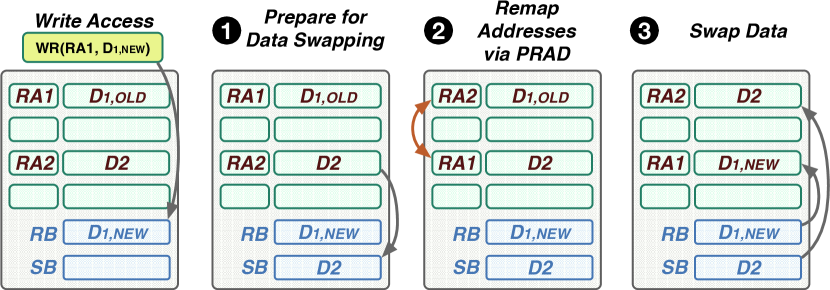
Figure 5 shows the sequence of commands required by the WoLFRaM controller to remap and swap a memory block after a write access from the CPU. We explain the process with a five-step example.
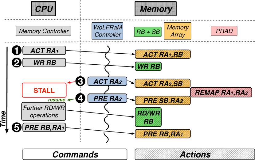
First, the memory controller issues an ACT command that reads block from the memory array into the row buffer (RB) . Second, the memory controller issues a WR command that writes the new data into the RB . Third, the WoLFRaM controller detects the WR command from the CPU and starts the remap and swap operation by selecting a random block () and issuing an ACT command that brings the content of into the swap buffer (SB) . This step also executes the key operation of reprogramming the PRAD to switch and addresses. To avoid conflicting commands from the memory controller, the WoLFRaM controller signals the memory controller to stop issuing commands to the memory bank (STALL) while the remap and swap operation is executing. Fourth, the WoLFRaM controller issues a PRE command that writes back the content of SB into its original address , which is now placed where was placed before the remapping operation. As the WoLFRaM controller completes the PRE command, it sends a resume signal to the memory controller, indicating that it can issue commands to the memory bank again. Fifth, the memory controller issues a PRE command that writes back the content of RB into its original address , which is now placed where was placed before the remapping operation. At the end of this process, the two blocks are effectively swapped in the physical space. Note that the memory controller can issue regular RD/WR commands freely if the PRAD is not being reprogrammed.
Remapping and Swapping Subarrays. When a subarray receives many write accesses, WoLFRaM might decide to remap and swap the entire subarray (see Section 3.1.2). The process consists of two main steps. First, WoLFRaM selects a random subarray to perform the remap and swap operation. Second, WoLFRaM controller issues remap and swap commands to all blocks in the subarray. Because all subarrays in a bank share the row buffer [38, 70, 71, 115, 50, 51] and the swap buffer, the remap and swap operation of each individual block is similar to the remap and swap operation within a subarray. The difference is that for remapping and swapping a subarray, WoLFRaM reprograms the global PRAD instead of the local PRAD (see Figure 1).
3.1.2 Remapping and Swapping Frequency
To limit the performance impact of the remap and swap operations and additional PRAD wear caused by extra programming operations, WoLFRaM remaps and swaps at a sufficiently low frequency. The WoLFRaM controller implements this mechanism by generating a random number (e.g., via a mechanism similar to D-RaNGe [44]) on every write access. If the generated number is less than or equal to threshold , WoLFRaM remaps and swaps the write address within the subarray, and if it is less than or equal to threshold , WoLFRaM remaps and swaps the entire subarray. The higher the and thresholds, the faster the wear-leveling, at the cost of higher performance and energy overheads. In our evaluation, the threshold is much lower than , as remapping an entire subarray is much more costly than remapping a single memory block (e.g., 512 energy and performance overhead). Previous works propose similar randomized swapping techniques in the context of wear-leveling for flash memories [6] and PCM as secure main memory [95]. Our evaluation (Section 5.3) shows that WoLFRaM performance overhead is very low.
3.1.3 Preventing Wear-Out Attacks
WoLFRaM is secure against attacks that try to wear out a particular memory position. The probabilistic approach implemented in WoLFRaM renders such an attack impractical, since the remapping intervals are entirely random. We quantitatively demonstrate this in Section 5.2 for the repeated address attack.
Unlike WoLFRaM, simple wear-leveling approaches [88, 82] use a constant remapping interval that triggers subarray-level remapping exactly every write access. Such approaches create an opportunity for malicious exploits [95]: after inferring the remapping interval size , the attacker may wear a certain memory position by writing to it times, and changing the address on the write, so the mechanism remaps an unrelated address. The attacker can repeat this procedure during every remapping cycle, which can significantly reduce the efficiency of the wear-leveling mechanism.
3.2 WoLFRaM Fault Tolerance
WoLFRaM fault tolerance mechanism can recover from a memory block failure by remapping such a failed memory block to an empty (unoccupied or spare) memory block. WoLFRaM tracks empty memory blocks in hardware using an additional bit that is set when a new address is programmed into the PRAD, and reset when a data block is deleted.
WoLFRaM detects failures via read-after-write verification [82]. In WoLFRaM, a memory block failure does not require mapping-out an entire page as proposed by many resistive memory fault tolerance mechanisms [87, 26, 81, 5, 35, 89]. WoLFRaM enables fine-grained remapping at memory block granularity), which allows the memory to continue operating transparently while its capacity reduces with the number of memory block failures.
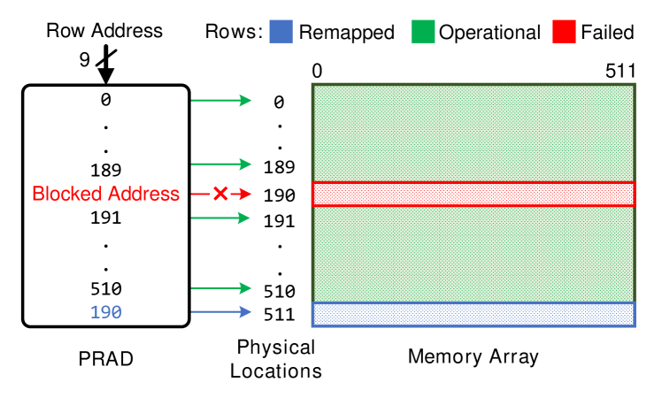
A failed memory block is remapped by (1) physically disabling the PRAD row associated with it, and (2) reprogramming its address into an empty PRAD row. As a result, the address of the memory block remains the same although its physical location changes.
Block failures. Figure 6 illustrates how WoLFRaM repairs a memory block failure within a subarray where all addresses are originally programmed to match their physical locations. When WoLFRaM detects a failed memory block, it remaps the failed memory block to an empty row in the subarray. In the example of the Figure 6, WoLFRaM programs the address of the failed block into the empty row at the bottom of the subarray. After that point, the physical address is marked as blocked and never accessed again (i.e., it is mapped out of the address space).
Subarray failures. If a subarray experiences a terminal failure (e.g., most of its memory blocks fail), it can be remapped to an empty subarray by reprogramming the global PRAD.
3.3 Combining WoLFRaM with Existing Fault Correction Techniques
WoLFRaM is compatible with many state-of-the-art fault correction techniques, which allows tolerating more than one fault per memory block.
We briefly discuss two fault correction techniques that can be easily integrated with WoLFRaM. First, WoLFRaM can be combined with ECP [87] by replacing the hardwired address decoder of the memory device with PRAD. ECP stores several error correcting pointers in each memory block and replaces failed cells with redundant ones. Unlike the original ECP paper [87], WoLFRaM does not require recovering a terminal memory block failure by decommissioning the entire page. Instead, WoLFRaM simply remaps the failed memory block to a known-operational memory location.
3.4 Putting it All Together: Wear-Leveling + Fault Tolerance
When a memory block fails and is mapped out (i.e., its address is removed from the address space), the wear-leveling mechanism should no longer use this address for remapping. WoLFRaM resolves this issue by simply OR-ing all row-selects in the PRAD. The OR Output ’0’ indicates that there is no matching decoder position (i.e., the looked-up address belongs to a mapped-out block), so the wear-leveling controller reattempts the remapping. Since no actual write is made into a mapped-out location, the performance overhead of WoLFRaM’s remapping attempt is negligible.
State-of-the-art fault tolerance techniques [87, 89, 26, 113, 81, 5, 35] do not discuss how wear-leveling can continue operating seamlessly after a failed memory block is mapped out. Once a block fails, the assumption that any address can be remapped to any other address is no longer valid [25]. One way to solve this problem is to detect mapped-out locations by checking failures in the read-after-write verification process. If the verification fails, the wear-leveling mechanism should reattempt the remapping and writing. This approach incurs additional performance overhead due to the additional write operations.
3.5 WoLFRaM Controller
There are several ways to implement the WoLFRaM controller in a resistive memory system. We use a WoLFRaM controller per memory bank, and we place all WoLFRaM controllers in one separate chip in the memory module (similar to [93]). Each WoLFRaM controller can issue memory commands to its associated memory bank, and its operation is independent of the other WoLFRaM controllers for different banks. We find two main challenges in implementing the WoLFRaM controller.
First, every time the WoLFRaM controller executes a remap and swap operation, it needs to notify to the memory controller that it should not issue any command to the memory bank while the swap and remap operation is executing. To enable the synchronization between the WoLFRaM controller and the memory controller, we add a new pin in the DRAM module. Before the remap and swap operation starts, the WoLFRaM controller sends a synchronization signal on this pin to indicate that commands from the memory controller to the bank should stall. When the remap and swap operation finishes, the WoLFRaM controller sends a synchronization signal on the same pin to indicate that commands from the memory controller to the bank can resume.
Second, WoLFRaM uses a a probabilistic approach to remap and swap memory blocks (Section 3.1.2), which requires generating random numbers. We use a true random number generator (TRNG), called D-RaNGe [44], that reduces the memory access latency below reliable values and exploits memory cells’ failure probability to generate random numbers. WoLFRaM controller 1) generates random numbers when the chip is idle, 2) compares the generated random values to and thresholds to decide if it needs to remap and swap future write accesses, and 3) it stores its decisions in a small array of bits. An alternative implementation is to use a pseudo-random number generator (PRNG) [106], which uses a deterministic algorithm to generate a sequence of random numbers from a seed value. A PRNG avoids adding a new pin to the memory module for synchronization: we can synchronize the WoLFRaM controller and the memory controller by implementing the same PRNG in both controllers, and sharing the same seed, which allows the memory controller to know when and for how long to stall. 222The drawback of using a PRNG is that a malicious attacker can reproduce the sequence of generated random numbers if they are able to obtain the PRNG seed, which could compromise the system. We choose to use a TRNG instead of a PRNG for security reasons.
4 Experimental Setup
We evaluate the lifetime of resistive memories by using an in-house simulator. We compare WoLFRaM with two-level Security Refresh (SR) [88]. SR is a dynamic randomized address mapping scheme that swaps data using random keys upon each refresh. To ensure lifetime evaluation fairness, we select the design and simulation parameters such that WoLFRaM and SR have similar area, performance and energy overheads.
We configure SR following the assumptions made by the original paper [88]. For practical purposes, we select slightly suboptimal number of SR subregions (2,048 instead of the optimal SR subregion count of 1,024 [88]). This allows confining the subregion to a single subarray, which significantly reduces the complexity of address generation. Since SR performs two extra writes per swap [88] ( one extra write per intra-subarray swap with WoLFRaM, as explained in Section 3.1.1), we apply an inner SR refresh interval of 200 write accesses to ensure a fair comparison. The outer SR refresh interval is set to 100 write accesses, on par with the average WoLFRaM inter-subarray remapping interval.
We configure WoLFRaM for remapping individual memory blocks with =1% probability (i.e., the average remapping interval is 100 write accesses), because it provides a good trade-off between performance overhead and wear-leveling. We choose to remap an entire subarray with a probability =0.002% (i.e., the average remapping interval is 512x100 write accesses) such that the performance overhead is similar to that of individual memory block remapping.
We calculate the area of the swap buffer (SB) used in our evaluation by using data from prior work [50]. We evaluate the energy and latency of PRAD using Cadence Virtuoso [105] with a 28nm high-K metal gate library from GlobalFoundries. We verify the functionality of PRAD, and simulate its timing and energy consumption using SPICE simulations [75].
Table 1 shows the latency and energy of the baseline 9-to-512 NAND hardwired address decoder and the 9-to-512 NAND PRAD we use in our evaluation. We also show the overhead of PRAD compared to a hardwired address decoder, and compared to the entire memory subarray.
| Hardwired Address Decoder | PRAD | PRAD/ Hardwired Decoder Overhead | PRAD/Memory Subarray Overhead | |
| Latency | 112.2 ps | 112.7 ps | 0.44% | 0.09% |
| Energy | 0.54 pJ | 0.63 pJ | 18% | 0.07% |
We assume that a memory cell lifetime (i.e., write endurance) is normally distributed with the mean of writes and coefficient of variation of 15%, similar to previous works [88, 82, 81, 113, 83].
Performance. To evaluate performance, we use the state-of-the-art extensible DRAM simulator Ramulator [46, 86] extended to support PRAD. We open-source our simulator and all configurations used for collecting our results [1]. To collect the Ramulator input memory traces, we use Intel’s dynamic binary instrumentation tool, Pin [63], for all the benchmarks described in Section 4.1.
Table 2 shows the configuration of the PCM memory system. Each 1GB bank has a row size of 1KB and consists of rows [88]. The interface used by the memory controller is LPDDR2-NVM-based [39], where each read/write is a burst of eight 64b transfers (i.e., 64B per request) [56, 45, 55].
| Memory Type | Phase Change Memory (PCM) | ||
| Banks | 1 GB capacity, 1KB ( bits) row size, rows | ||
| I/O |
|
Table 3 shows the timing and energy parameters of the PCM memory used as main memory in our evaluation. To ensure a fair comparison with Security Refresh, the timing and energy values are based on the data provided in [50].
| Operation | Energy (pJ/bit) |
| Array read | 2.47 |
| Array write | 16.82 |
| Buffer read | 0.93 |
| Buffer write | 1.03 |
| Standby | 0.08 |
| Timing parameters | Cycles |
| tRCD, tCL, tWL, tCCD, tWTR | 22, 5, 4, 4, 3 |
| tWR, tRTP, tRP, tRRDact, tRRDpre | 6, 3, 60, 2, 11 |
Table 4 shows the CPU configuration used in our Ramulator simulations. We obtain results by running each simulation for 1.4 billion instructions, after 1 million warmup instructions.
| Processor | Single-core, 2.4GHz, L1-I 32kiB, L1-D 32kiB, L2 2MiB, L3 16MiB |
| Memory controller | 32 |
| R/W Queue Size | |
| Memory Scheduler | FRFCFS with cap of 16 on row hits [73, 99, 100, 74] |
| Address translation | MSB to LSB: Row Bank Rank Column Channel |
Energy. To evaluate the WoLFRaM energy consumption, we use an in-house energy estimation tool connected to Ramulator that estimates the read/write energy based on parameters from [50], summarized in Table 1 and Table 3.
4.1 Workloads
Attack test. For memory lifetime evaluation, we use a repeated address attack test that repeatedly writes to the same memory location [88]. This test is the simplest malicious wear-out attack.
SPEC CPU2006. For performance and energy overhead evaluation, we use 28 benchmarks from SPEC CPU2006 [30].
5 Evaluation
5.1 Area Overhead
Table 5 shows the area overhead of the evaluated mechanisms relative to the size of a PCM memory subarray. At the top part of the table we show the overheads of the evaluated mechanisms alone (SR, WoLFRaM). At the bottom part of the table we show the overheads of the same mechanisms when combined with ECP error correction [87]. An error correction mechanism can correct k failed bits in an individual memory block with an area overhead of approximately % [87].
| Mechanism | Area Overhead (in Subarray) |
| SR | 0.02% |
| WoLFRaM | 0.95% |
| 1.90% | |
| 13.33% | |
| 12.85% |
Our results show that the area overhead of WoLFRaM is slightly below 0.95%, of which 0.85% is from PRADs, and 0.1% is from the rest of the hardware components. Although the area overhead of WoLFRaM is higher than that of SR, WoLFRaM provides better protection against errors (i.e., both wear-leveling and fault tolerance as we show in Section 5.2).
For approximately the same area overhead, WoLFRaM can be combined with (6-bit correction), and SR can be combined with (7-bit correction). In addition to ECP capabilities, differs from in that the latter maps out the entire page that contains the failed memory block. In contrast, WoLFRaM enables decommissioning individual failed memory blocks, which allows more graceful memory capacity degradation.
5.2 Memory Lifetime with Wear-Leveling,
Fault Tolerance, and Error Correction
To evaluate the relative effectiveness of the wear-leveling, fault tolerance, and error correction techniques, the metric we use is usable memory capacity as a function of the memory lifetime. The higher the memory capacity at any given point in the memory lifetime, the more effective the combined wear-leveling, fault tolerance, and error correction techniques.
Although SR is not able to handle wear-leveling after mapping out memory pages, we assume it can continue its operation. This requires applying additional resources to make the combined SR+ work [25], whose overheads we do not account for so that we give the benefit of doubt to SR.
Figure 7 presents usable memory capacity as a function of lifetime for , , WoLFRaM with no error correction and , when executing the attack test workload (Section 4.1). We assume that the memory device is decommissioned after its usable capacity declines by half.
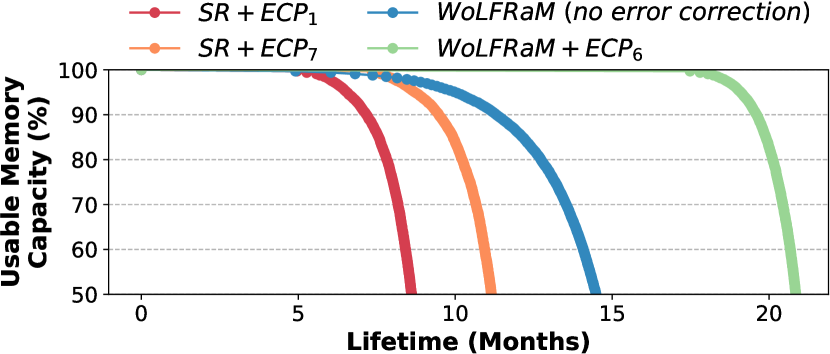
We make two observations. First, the memory lifetime of is 87% longer than that of state-of-the-art , using a similar area overhead (12.85% 13.33%). Second, the memory lifetime of WoLFRaM with no added error correction capabilities is 68% longer than that of , using slightly less area overhead (0.95% 1.90%). We conclude that WoLFRaM achieves significantly longer lifetime than the state-of-the-art mechanism for similar area overhead.
An additional advantage of WoLFRaM is the wear-leveling speed. A quick leveling of write non-uniformity is important and might become critical when there is significant endurance variation across memory banks. In wear-leveling solutions where remapped addresses are independent of write accesses, such as SR, it takes considerable time for a data block to be remapped. This means that especially "weak" cells may fail before their addresses are remapped. In contrast, WoLFRaM chooses to remap frequently-written addresses, which allows faster remapping of cells that have a higher probability to fail.
Figure 8 shows the per-row write count histogram for WoLFRaM (=1% and =10%) , and single-level SR, using the attack test (Section 4.1). The ideal wear-leveling mechanism would reach an identical number of per-row writes in each memory row, producing a single vertical bar in the per-row write count histogram. The narrower the distribution, the more effective the wear-leveling mechanism is. We make the key observation that WoLFRaM is significantly more effective than SR, and WoLFRaM =10% is very close to the ideal wear-leveling mechanism.
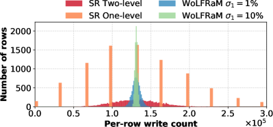
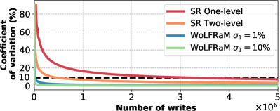
Figure 9 shows the coefficient of variation (CoV) of the per-row write count distribution as a function of the number of write accesses. The sharper the drop, the quicker the write nonuniformity leveling is. We make the key observation that WoLFRaM converges much faster than SR. WoLFRaM (=1%) has 90% CoV drop after 21,969 write accesses, which is 21.7× faster than the two-level SR mechanism and 147.1x faster than the one-level SR mechanism. We conclude that WoLFRaM levels the write nonuniformity significantly faster than the state-of-the-art wear-leveling mechanisms.
5.3 Performance and Energy Overheads
Figure 10 shows the performance and energy overheads of WoLFRaM when running SPEC CPU2006 benchmarks, with the configuration described in Section 4. We make two main observations. First, the average performance degradation caused by WoLFRaM is only 0.51%, and the worst performance degradation is 3.8% (in 429.mcf). Also, there are 9 benchmarks (e.g., 444.ramd) that have negligible overhead. Second, the average WoLFRaM energy overhead is only 0.47%, and the worst energy overhead is only 2.1% (429.mcf). Also, there are 9 benchmarks that have negligible energy overhead.
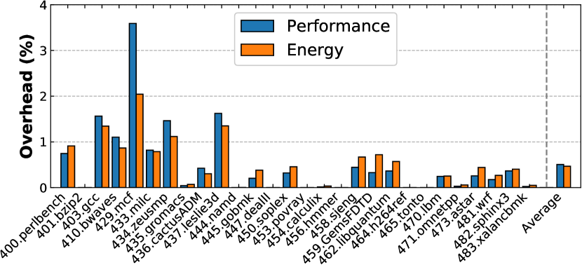
We conclude that performance and energy overheads of WoLFRaM are very low, and for many benchmarks the overheads are negligible, which makes WoLFRaM a low-cost mechanism to expand the lifetime of resistive memories.
5.4 PRAD Wearout
During WoLFRaM operation, local PRAD is reprogrammed once every writes on average (see Section 3.1.3). Hence, local PRADs wear out at a rate times slower than the memory array (e.g., for %, 100x slower). The global PRAD is reprogrammed every 1/ () writes on average, which makes its wear out negligible compared to the wear out of the resistive memory cells.
6 Related Work
To our knowledge, WoLFRaM is the first work that seamlessly integrates wear-leveling and fault tolerance techniques in the same mechanism. We have already discussed and evaluated Security Refresh [88] in Sections 4 and 5. We now briefly discuss other resistive memory techniques for enhancing lifetime, wear-leveling and fault tolerance.
6.1 Wear-Leveling Techniques
Wear-Leveling Techniques for PCM. There are many prior works that propose wear-leveling techniques to enhance PCM lifetime [121, 41, 95, 82, 88, 83, 116, 117, 25, 29, 122, 120, 22, 21, 62, 61, 77, 2, 34, 23]. These works propose different techniques to optimize wear-leveling via swapping and remapping data. Several prior works propose wear-leveling mechanisms that are aware of process variation across the memory chip [29, 122, 120]. Several techniques use OS support to improve PCM wear-leveling [22, 21, 62, 61, 77, 2, 34, 23].
Unlike WoLFRaM, none of these works implement or discuss how to integrate a fault tolerance mechanism that works with the proposed wear-leveling techniques. Also, some of these techniques require storing and maintaining large remapping tables [95, 121] , which can incur significant storage and latency overhead.
Wear-Leveling Techniques for Hybrid DRAM/PCM Memory. DRAM/PCM hybrid memories aim to provide the best of both worlds: the low access latency of DRAM, and the large storage capacity of PCM. Existing wear-leveling techniques 1) minimize the number of writes by reducing the number of dirty evictions to PCM and re-compute results instead of saving data in PCM [31], 2) use techniques to allocate heavily-written data in DRAM only [60, 114], or 3) migrate heavily-written pages from PCM to DRAM [119]. WoLFRaM can be combined with these techniques to further improve wear-leveling effectiveness.
6.2 Fault Tolerance and Error Correction
There are many fault tolerance and error correction techniques that can be applied to resistive memories [87, 81, 102, 89, 26, 69, 35, 5, 103, 113, 4, 104, 57, 59, 58, 80, 17, 78, 79, 47, 76, 48, 13, 12, 66, 16, 15, 67, 9, 14, 11, 10, 64, 65, 8, 7, 111, 112, 108, 107, 3, 42]. Among these works, there are several that focus specifically on resistive memories [87, 81, 102, 89, 26, 69, 35, 5, 103, 113] that can be classified into four categories. First, techniques that replace faulty cells with redundant cells [87, 81, 102]. Second, techniques that use data partitioning and inversion [89, 26, 69, 118]. SAFER [89], Aegis [26], RDIS [69], and Zhang et al. [118] exploit the observation that a stuck-at-value memory cell remains readable, and employ data partitioning and inversion of faulty partitions to tolerate cell failures. Third, techniques that use faulty page and block pairing. DRM [35] tolerates block failures within a page by pairing it with another page such that failed blocks do not intersect. Zombie memory [5] corrects errors in memory blocks by pairing them with working blocks of decommissioned pages. Block Cooperation [103] repurposes faulty blocks to provide support to working blocks within the same page to keep the page “alive”. Fourth, techniques that use ECC. FREE-p [113] performs fine-grained remapping of memory blocks by storing remapping pointers in the functional cells of a worn-out block. FREE-p protects against both hard and soft errors. Unlike WoLFRaM, none of these mechanisms consider the integration of a wear-leveling mechanism with a fault tolerance or error correction mechanism, which is essential to make these mechanisms work in real systems.
6.3 Other Lifetime Enhancement Mechanisms
Device-Level Techniques. Several works use device-level techniques to improve resistive memory lifetime [40, 96]. Jiang et al. [40] propose using the 2-bit MLC cell as a tristate cell to reduce the RESET current to increase PCM endurance. This technique can be used together with WoLFRaM to further improve memory lifetime.
Reducing Redundant Writes. Many prior works improve PCM lifetime by reducing the number of written bits into memory [50, 121, 41, 24, 101, 52]. Some works [50, 121, 41, 24] propose writing to the memory array only those bits whose values had been changed in the row buffer, which reduces the number of cells modified on each write. All these techniques can be used together with WoLFRaM to further improve memory lifetime.
7 Conclusion
We propose WoLFRaM, the first mechanism that combines wear-leveling and fault tolerance seamlessly and efficiently in resistive memories. WoLFRaM wear-leveling mechanism remaps writes on-the-fly to random locations, and WoLFRaM fault tolerance mechanism remaps a failed memory block to an empty (unoccupied or spare) memory block.
Unlike previous works, WoLFRaM integrates both mechanisms efficiently using a programmable resistive address decoder (PRAD), which decouples memory addresses from physical memory locations. WoLFRaM enables rapid leveling of the write non-uniformity, and fine-grained remapping of faulty memory blocks.
Our evaluations show that WoLFRaM combined with (error correcting pointers) provides 68% longer lifetime, and WoLFRaM combined with provides 87% longer lifetime, compared to the best state-of-the-art wear-leveling mechanism and fault correction techniques, for similar or less area overhead. The average performance (energy) penalty of WoLFRaM is 0.51% (0.47%), compared to a baseline system without any wear-leveling or fault tolerance techniques. We conclude that WoLFRaM is an effective and low-cost reliability solution for resistive memories.
Acknowledgements
We thank the SAFARI Research Group members for the valuable input and the stimulating intellectual environment they provide, the anonymous reviewers for their feedback, and the industrial partners of SAFARI, especially ASML, Google, Huawei, Intel, Microsoft, and VMware, for their support.
References
- [1] “Ramulator-WoLFRaM Source Code,” https://github.com/suyashmahar/ramulator-wolfram, 2020.
- [2] H. Aghaei Khouzani et al., “Prolonging PCM lifetime through energy-efficient, segment-aware, and wear-resistant page allocation,” ISLPED, 2014.
- [3] A. R. Alameldeen et al., “Energy-efficient cache design using variable-strength error-correcting codes,” ISCA, 2011.
- [4] M. Awasthi et al., “Efficient scrub mechanisms for error-prone emerging memories,” HPCA, 2012.
- [5] R. Azevedo et al., “Zombie memory: Extending memory lifetime by reviving dead blocks,” ISCA, 2013.
- [6] A. Ben-Aroya and S. Toledo, “Competitive analysis of flash-memory algorithms,” ESA, 2006.
- [7] Y. Cai et al., “Error characterization, mitigation, and recovery in flash-memory-based solid-state drives,” Proceedings of the IEEE, 2017.
- [8] Y. Cai et al., “Errors in flash-memory-based solid-state drives: Analysis, mitigation, and recovery,” Inside Solid State Drives, 2018.
- [9] Y. Cai et al., “Vulnerabilities in MLC NAND flash memory programming: Experimental analysis, exploits, and mitigation techniques,” HPCA, 2017.
- [10] Y. Cai et al., “Error patterns in MLC NAND flash memory: Measurement, characterization, and analysis,” DATE, 2012.
- [11] Y. Cai et al., “Threshold voltage distribution in MLC NAND flash memory: Characterization, analysis, and modeling,” DATE, 2013.
- [12] Y. Cai et al., “Read disturb errors in MLC NAND flash memory: Characterization, mitigation, and recovery,” DSN, 2015.
- [13] Y. Cai et al., “Data retention in MLC NAND flash memory: Characterization, optimization, and recovery,” HPCA, 2015.
- [14] Y. Cai et al., “Program interference in MLC NAND flash memory: Characterization, modeling, and mitigation,” ICCD, 2013.
- [15] Y. Cai et al., “Flash correct-and-refresh: Retention-aware error management for increased flash memory lifetime,” ICCD, 2012.
- [16] Y. Cai et al., “Neighbor-cell assisted error correction for MLC NAND flash memories,” SIGMETRICS, 2014.
- [17] L. B. Capps Jr and T. Nguyen, “Method and apparatus for optimizing ECC memory performance,” US Patent 5,961,660. Oct. 5 1999.
- [18] K. K. Chang et al., “Understanding latency variation in modern DRAM chips: Experimental characterization, analysis, and optimization,” SIGMETRICS, 2016.
- [19] K. K. Chang et al., “Low-cost inter-linked subarrays (LISA): Enabling fast inter-subarray data movement in DRAM,” HPCA, 2016.
- [20] K. K.-W. Chang et al., “Improving DRAM performance by parallelizing refreshes with accesses,” HPCA, 2014.
- [21] Y.-M. Chang et al., “Improving PCM Endurance with a Constant-Cost Wear Leveling Design,” TODAES, 2016.
- [22] C.-H. Chen et al., “Age-based PCM wear leveling with nearly zero search cost,” DAC, 2012.
- [23] S. W. Cheng et al., “Efficient Warranty-Aware Wear Leveling for Embedded Systems With PCM Main Memory,” VLSI, 2016.
- [24] S. Cho and H. Lee, “Flip-N-Write: A Simple Deterministic Technique to Improve PRAM Write Performance , Energy and Endurance,” MICRO, 2009.
- [25] J. Fan et al., “WL-Reviver: A Framework for Reviving any Wear-Leveling Techniques in the Face of Failures on Phase Change Memory,” DSN, 2014.
- [26] J. Fan et al., “Aegis: Partitioning data block for efficient recovery of stuck-at-faults in phase change memory,” MICRO, 2013.
- [27] S. Ghose et al., “Demystifying complex workload-DRAM interactions: An experimental study,” SIGMETRICS, 2019.
- [28] R. W. Hamming, “Error detecting and error correcting codes,” The Bell system technical journal, 1950.
- [29] Y. Han et al., “Enhanced wear-rate leveling for PRAM lifetime improvement considering process variation,” VLSI, 2015.
- [30] J. L. Henning, “SPEC CPU2006 benchmark descriptions,” CAN, 2007.
- [31] J. Hu et al., “Write activity minimization for nonvolatile main memory via scheduling and recomputation,” TCAD, 2011.
- [32] J. Hu et al., “Reducing write activities on non-volatile memories in embedded CMPs via data migration and recomputation,” DAC, 2010.
- [33] H. Huh et al., “A 64Gb NAND Flash Memory with 800MB/s Synchronous DDR Interface,” IMW, 2012.
- [34] S. Im and D. Shin, “Differentiated space allocation for wear leveling on phase-change memory-based storage device,” TCE, 2014.
- [35] E. Ipek et al., “Dynamically replicated memory: building reliable systems from nanoscale resistive memories,” ASPLOS, 2010.
- [36] J. Izraelevitz et al., “Basic Performance Measurements of the Intel Optane DC Persistent Memory Module,” 2019.
- [37] JEDEC, “JEDEC Standard 21-C, Section 4.1.2.11 Serial Presence Detect (SPD) for DDR3 SDRAM Modules,” JEDEC, Tech. Rep., 2008. https://www.jedec.org/standards-documents/docs/jesd-15-1
- [38] JEDEC Standard, “Low power double data rate 2 (LPDDR2),” JESD209-2E, April, 2011.
- [39] JEDEC Standard, “Low-Power Double Data Rate 2 Non-Volatile Memory,” JESD209-F, 2013.
- [40] L. Jiang et al., “ER: Elastic RESET for Low Power and Long Endurance MLC based Phase Change Memory,” ISLPED, 2012.
- [41] Y. Joo et al., “Energy- and endurance-aware design of phase change memory caches,” DATE, 2010.
- [42] S. Khan et al., “The efficacy of error mitigation techniques for DRAM retention failures: A comparative experimental study,” SIGMETRICS, 2014.
- [43] J. Kim et al., “Solar-DRAM: Reducing DRAM access latency by exploiting the variation in local bitlines,” ICCD, 2018.
- [44] J. S. Kim et al., “D-RaNGe: Using commodity DRAM devices to generate true random numbers with low latency and high throughput,” HPCA, 2019.
- [45] Y. Kim et al., “A case for exploiting subarray-level parallelism (SALP) in DRAM,” ISCA, 2012.
- [46] Y. Kim et al., “Ramulator: A fast and extensible DRAM simulator,” CAL, 2015.
- [47] D. Kline et al., “Flower and fame: A low overhead bit-level fault-map and fault-tolerance approach for deeply scaled memories,” HPCA, 2020.
- [48] D. Kline et al., “Sustainable fault management and error correction for next-generation main memories,” IGSC, 2017.
- [49] E. Kültürsay et al., “Evaluating STT-RAM as an energy-efficient main memory alternative,” ISPASS, 2013.
- [50] B. C. Lee et al., “Architecting phase change memory as a scalable DRAM alternative,” ISCA, 2009.
- [51] B. C. Lee et al., “Phase change memory architecture and the quest for scalability,” CACM, 2010.
- [52] B. C. Lee et al., “Phase-change technology and the future of main memory,” IEEE Micro, 2010.
- [53] D. Lee et al., “Design-induced latency variation in modern DRAM chips: Characterization, analysis, and latency reduction mechanisms,” POMACS, 2017.
- [54] D. Lee et al., “Adaptive-latency DRAM: Optimizing DRAM timing for the common-case,” HPCA, 2015.
- [55] D. Lee et al., “Tiered-latency DRAM: A low latency and low cost DRAM architecture,” HPCA, 2013.
- [56] D. Lee et al., “Decoupled direct memory access: Isolating CPU and IO traffic by leveraging a dual-data-port DRAM,” PACT, 2015.
- [57] S. Li et al., “System implications of memory reliability in exascale computing,” SC, 2011.
- [58] S. Li et al., “Selective error correcting code and memory access granularity switching,” US Patent 10,318,365. Jun. 11 2019.
- [59] S. Li et al., “MAGE: Adaptive granularity and ECC for resilient and power efficient memory systems,” in SC, 2012.
- [60] Y. Li et al., “A software approach for combating asymmetries of non-volatile memories,” ISLPED, 2012.
- [61] D. Liu et al., “Application-Specific Wear Leveling for Extending Lifetime of Phase Change Memory in Embedded Systems,” IEEE TCAD, 2014.
- [62] L. Long et al., “A space-based wear leveling for PCM-based embedded systems,” RTCSA, 2013.
- [63] C.-K. Luk et al., “Pin: Building Customized Program Analysis Tools with Dynamic Instrumentation,” PLDI, 2005.
- [64] Y. Luo et al., “WARM: Improving NAND flash memory lifetime with write-hotness aware retention management,” MSST, 2015.
- [65] Y. Luo et al., “Enabling accurate and practical online flash channel modeling for modern MLC NAND flash memory,” JSAC, 2016.
- [66] Y. Luo et al., “HeatWatch: Improving 3D NAND flash memory device reliability by exploiting self-recovery and temperature awareness,” HPCA, 2018.
- [67] Y. Luo et al., “Improving 3D NAND flash memory lifetime by tolerating early retention loss and process variation,” SIGMETRICS, 2018.
- [68] Y. Luo et al., “Characterizing application memory error vulnerability to optimize datacenter cost via heterogeneous-reliability memory,” DSN, 2014.
- [69] R. Melhem et al., “RDIS: A recursively defined invertible set scheme to tolerate multiple stuck-at faults in resistive memory,” DSN, 2012.
- [70] J. Meza et al., “A Case for Small Row Buffers in Non-volatile Main Memories,” ICCD, 2012.
- [71] J. Meza et al., “Evaluating Row Buffer Locality in Future Non-volatile Main Memories,” SAFARI Technical Report No. 2012-002, 2012.
- [72] J. Meza et al., “A Case for Efficient Hardware-Software Cooperative Management of Storage and Memory,” WEED, 2013.
- [73] O. Mutlu and T. Moscibroda, “Stall-time fair memory access scheduling for chip multiprocessors,” MICRO, 2007.
- [74] O. Mutlu and T. Moscibroda, “Parallelism-aware batch scheduling: Enhancing both performance and fairness of shared DRAM systems,” ISCA, 2008.
- [75] L. W. Nagel and D. Pederson, “SPICE (Simulation Program with Integrated Circuit Emphasis),” EECS Department, University of California, Berkeley, Tech. Rep., Apr 1973.
- [76] P. J. Nair et al., “ArchShield: Architectural framework for assisting DRAM scaling by tolerating high error rates,” ISCA, 2013.
- [77] C. Pan et al., “Wear-Leveling Aware Page Management for Non-Volatile Main Memory on Embedded Systems,” TMSCS, 2016.
- [78] M. Patel et al., “Understanding and modeling on-die error correction in modern DRAM: An experimental study using real devices,” DSN, 2019.
- [79] M. Patel et al., “Bit-exact ECC recovery (BEER): Determining DRAM on-die ECC functions by exploiting DRAM data retention characteristics,” MICRO, 2020.
- [80] F. Qin et al., “SafeMem: Exploiting ECC-memory for detecting memory leaks and memory corruption during production runs,” HPCA, 2005.
- [81] M. K. Qureshi, “Pay-As-You-Go: low-overhead hard-error correction for phase change memories,” MICRO, 2011.
- [82] M. K. Qureshi et al., “Enhancing lifetime and security of PCM-based main memory with start-gap wear leveling,” MICRO, 2009.
- [83] M. K. Qureshi et al., “Practical and secure pcm systems by online detection of malicious write streams,” HPCA, 2011.
- [84] M. K. Qureshi et al., “Scalable high performance main memory system using phase-change memory technology,” ISCA, 2009.
- [85] S. Raoux et al., “Phase-change random access memory: A scalable technology,” IBM JRD, 2008.
-
[86]
SAFARI Research Group, “Ramulator for processing-in-memory,”
https://github.com/CMU-SAFARI/ramulator-pim/, 2020. - [87] S. Schechter et al., “Use ECP, not ECC, for hard failures in resistive memories,” ISCA, 2010.
- [88] N. H. Seong et al., “Security refresh: prevent malicious wear-out and increase durability for phase-change memory with dynamically randomized address mapping,” ISCA, 2010.
- [89] N. H. Seong et al., “SAFER: Stuck-at-fault error recovery for memories,” MICRO, 2010.
- [90] V. Seshadri et al., “Fast bulk bitwise AND and OR in DRAM,” CAL, 2015.
- [91] V. Seshadri et al., “RowClone: fast and energy-efficient in-DRAM bulk data copy and initialization,” MICRO, 2013.
- [92] V. Seshadri et al., “Ambit: In-memory accelerator for bulk bitwise operations using commodity DRAM technology,” MICRO, 2017.
- [93] V. Seshadri et al., “Gather-scatter DRAM: In-DRAM address translation to improve the spatial locality of non-unit strided accesses,” MICRO, 2015.
- [94] V. Seshadri and O. Mutlu, “In-DRAM bulk bitwise execution engine,” arXiv, 2019.
- [95] A. Seznec, “A phase change memory as a secure main memory,” CAL, 2010.
- [96] M. Shevgoor et al., “Improving memristor memory with sneak current sharing,” ICCD, 2015.
- [97] S. Song et al., “Enabling and exploiting partition-level parallelism (PALP) in phase change memories,” TECS, 2019.
- [98] S. Song et al., “Improving phase change memory performance with data content aware access,” ISMM, 2020.
- [99] L. Subramanian et al., “The blacklisting memory scheduler: Achieving high performance and fairness at low cost,” ICCD, 2014.
- [100] L. Subramanian et al., “BLISS: Balancing performance, fairness and complexity in memory access scheduling,” TPDS, 2016.
- [101] G. Sun et al., “A frequent-value based PRAM memory architecture,” ASP-DAC, 2011.
- [102] M. K. Tavana et al., “REMAP: A reliability/endurance mechanism for advancing PCM,” MEMSYS, 2017.
- [103] M. K. Tavana et al., “Block Cooperation: Advancing Lifetime of Resistive Memories by Increasing Utilization of Error Correcting Codes,” TACO, 2018.
- [104] A. N. Udipi et al., “Lot-ecc: Localized and tiered reliability mechanisms for commodity memory systems,” ISCA, pp. 285–296, 2012.
- [105] Virtuoso, “Virtuoso Analog Design Environment.” https://www.cadence.com/content/cadence-www/global/en_US/home/tools/custom-ic-analog-rf-design/circuit-design/virtuoso-analog-design-environment.html
- [106] J. Von Neumann, “Various techniques used in connection with random digits,” Appl. Math Ser, 1951.
- [107] C. Wilkerson et al., “Reducing cache power with low-cost, multi-bit error-correcting codes,” ISCA, 2010.
- [108] C. Wilkerson et al., “Trading off cache capacity for reliability to enable low voltage operation,” ISCA, 2008.
- [109] H.-S. P. Wong et al., “Phase change memory,” Proceedings of the IEEE, 2010.
- [110] L. Yavits et al., “Resistive address decoder,” CAL, 2017.
- [111] D. H. Yoon and M. Erez, “Virtualized and flexible ECC for main memory,” ASPLOS, 2010.
- [112] D. H. Yoon and M. Erez, “Virtualized ECC: Flexible reliability in main memory,” IEEE micro, 2010.
- [113] D. H. Yoon et al., “FREE-p: Protecting non-volatile memory against both hard and soft errors,” HPCA, 2011.
- [114] H. Yoon et al., “Row buffer locality aware caching policies for hybrid memories,” ICCD, 2012.
- [115] H. Yoon et al., “Efficient data mapping and buffering techniques for multilevel cell phase-change memories,” TACO, 2014.
- [116] H. Yu and Y. Du, “Increasing endurance and security of phase-change memory with multi-way wear-leveling,” TC, 2014.
- [117] J. Yun et al., “Bloom filter-based dynamic wear leveling for phase-change RAM,” DATE, 2012.
- [118] J. Zhang et al., “Dynamic partitioning to mitigate stuck-at faults in emerging memories,” ICCAD, 2017.
- [119] W. Zhang and T. Li, “Characterizing and mitigating the impact of process variations on phase change based memory systems,” MICRO, 2009.
- [120] X. Zhang and G. Sun, “Toss-up Wear Leveling: Protecting Phase-Change Memories from Inconsistent Write Patterns,” DAC, 2017.
- [121] P. Zhou et al., “A durable and energy efficient main memory using phase change memory technology,” ISCA, 2009.
- [122] W. Zhou et al., “Increasing lifetime and security of phase-change memory with endurance variation,” ICPAD, 2016.