Small-signal parameters extraction and noise analysis of CNTFETs
Abstract
The use of carbon nanotube (CNT) field-effect transistors (FETs) in microwave circuit design requires an appropriate, immediate and efficient description of their performance. This work describes a technique to extract the parameters of an electrical equivalent circuit for CNTFETs. The equivalent circuit is used to model the dynamic and noise performance at low- and high-frequency of different CNTFET technologies, considering extrinsic and intrinsic device parameters as well as the contact resistance. The estimation of the contact resistance at the metal/CNTs interfaces is obtained from a Y-function based extraction method. The noise model includes four noise sources: thermal noise, thermal channel noise, shot channel noise and flicker noise. The proposed model is compared with a compact model calibrated to hysteresis-free experimental data from a high-frequency multi-tube (MT)-CNTFET technology. Additionally, it has been applied to experimental data from another fabricated MT-CNTFET technology. The comparison in both cases shows a good agreement between reference data (simulation and experimental) and results from the proposed model. Low- and high-frequency noise projections of the fabricated reference device are further studied. Noise results from both studied technologies show that shot noise mainly contributes to the total noise due to the presence of Schottky barriers at contacts and along the channel.
Keywords: CNTFETs, small-signal, noise, modeling, contact resistance.
1 Introduction
Nowadays, silicon (Si) based technologies dominate the high-frequency electronic market. However, these components are reaching their performance limits, causing the search for new suitable solutions for high-performance applications, such as transistor technologies based on nanostructured materials. During the last years, carbon nanotube (CNT) field-effect transistors (FETs) have been studied in order to exploit their extraordinary inherent features, e.g., high-linearity [1, 2, 3, 4], low high-frequency noise [5, 6], quasi-ballistic transport and an outstanding gate control. Moreover, some projections refers to operation frequencies in the order of [7, 8], as the technological process improve and the limitations due to the fabrication are minimized (e.g., parasitics, growth methods and alignment of CNTs).
Fabricated CNTFET technologies with an extrinsic operation frequency of around have been reported in the literature [9, 10, 11]. These improvements have caused research efforts to develop radio-frequency (RF) applications using CNTFETs [12, 13, 14, 15]. The design of RF circuits based on CNTFET technologies requires a reliable compact model capable to reproduce the novel and unique behavior of the devices when these are used at circuit level computer-aided design. This compact model may help to understand and quantify the effect of parasitic elements on dynamic and noise performance. Also, this knowledge may highlight limitations in the fabrication process of the device, project ideal device performance at different bias conditions and can be useful to benchmark the device versus other technologies in specific scenarios.
The main problem related to the small-signal representation of an emergent transistor technology, such as CNTFETs, is the correct extraction of the parameters for the equivalent circuit, including the non-negligible contact resistances at metal/channel interfaces. As the development of a complete physics-based model for analog applications is challenging due to the presence of physical phenomena, such as potential barriers [13, 16] produced on the metal/CNT interface, as well as the non-linear behavior of the charge on the tubes [3, 16], CNTFET compact modeling is usually done by a semi-physical [17, 18] or by a semi-empirical approach [20, 21, 19], the latter is the approach followed here.
In this work, the equivalent circuit and the parameters extraction procedure, including the contact resistance extraction, are described in Section 2. The low- and high-frequency noise model as well as the description of the noise sources are presented in Section 3. The validation of the proposed model using a reference compact model is presented in Section 4. In Section 5 the proposed approach is applied to experimental data from a fabricated top-gated MT-CNTFET technology. Finally some conclusions are provided in Section 6.
2 Small-signal equivalent circuit and parameters extraction
2.1 Electrical equivalent circuit description
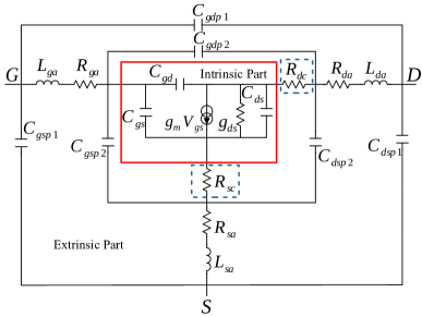
Fig. 1 introduces the equivalent circuit considered in this work, which is divided into three sections. The first one is the extrinsic part, which contains the parasitic parameters of the CNTFET, caused mainly by fabrication process issues, the second one is the intrinsic part, which represents the physical transport phenomena that occur inside the device through electrical parameters and the last one includes the contact resistances, related to the interfaces between CNTs in the channel and the metallic contacts, which are specially large in CNTFETs and can not be neglected due to their large impact in device performance [22, 23]. , , , , and are the extrinsic resistances and inductances associated to the access metallizations of the device for the gate, drain and source, respectively. and are the parasitic capacitances between gate and drain and between drain and source and and between gate and source. and are the contact resistances at the drain and source, respectively. In contrast to the parasitic parameters, contact resistances can not be de-embedded using standard procedures and are one of the most important CNTFETs fabrication issues, associated to Schottky barriers at the contacts [16], hence, in order to model accurately, the effect of contact resistances must be taken into account. The parameters related to the intrinsic part of the device are described as follows: is the channel or output conductance and is the transconductance, , and represent the intrinsic capacitances between the gate, drain and source and is the intrinsic voltage between gate and source.
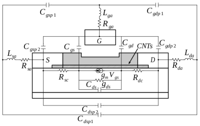
In Fig. 2, each parameter of the equivalent circuit is associated to the components of the cross-section schematic view for a top-gated CNTFET.
2.2 Extraction of the extrinsic parameters
A small output signal of a CNTFET used as an amplifier, an immediate analog application, can be easily affected by the parasitic elements. Thus, it is important to know appropriately the contribution of the extrinsic parameters and separate their contribution from that produced by the intrinsic parameters.
In order to extract correctly the extrinsic parameters of the device, it is necessary to use an accurate de-embedding procedure. The three-step parasitic de-embedding method is synthesized as in [25, 24] by equations (1) to (4).
| (1) |
| (2) |
| (3) |
| (4) |
where , and are the -parameters of an open, short and thru test structure, respectively. , and are the admittance outer-parasitics matrix, the admittance inner-parasitics matrix and the series-impedance parasitics matrix, respectively, (see Fig. 2 and eqs. (17) to (19) in [24]). represents the de-embedded -parameters. The three-step parasitic de-embedding method has been considered suitable to be applied to CNTFET characterization due to the high operation frequency expected in this technology [7, 8, 10, 11, 9] where an appropriate de-embedding method can improve accuracy of the device experimental data [24, 26].
Notice that the extracted extrinsic parameters do not consider the contribution of the contact resistances at the source and drain sides since these resistances are produced on the interface between CNTs and contact metallizations. Therefore, in order to have an accurate model for CNTFETs, the contribution of contact resistances is required to be removed by an additional process.
2.3 Contact resistance extraction
The total contact resistance () is an electrical representation of the physical phenomena at the junction metal/CNT at both drain and source contacts. This is one of the main issues that limits CNTFETs performance, thus it has to be considered in an accurate model. Also, an appropriate extraction can provide information about the contact quality to improve fabrication process and to project the performance of an optimized technology.
In order to perform an accurate extraction of the contact resistance of CNTFETs, a Y-function based method, labeled as YFM2 in [27], has been considered222Notice that the Y-function is defined as and has no relation with the admittance parameters discussed along this manuscript.. In contrast to the transfer length method (TLM), YFM2 does not require long CNT test structure [22] and only standard transfer characteristics in the linear region and at low drain bias of the device are required to extract . Also, a physics-based validation has been provided for this method in [27]. Despite the extracted resistance is not bias dependent, it can be considered as a reference value for near bias points as well as an upper limit value of for the device working in the active region.
As is stated in [27], in YFM2 the is extracted from the slope of once , and , the degradation factor of low-field carrier mobility and the extrinsic and intrinsic reduction mobility carrier coefficient, respectively, are extracted from the Y-function obtained from the drain current equation described in [27] (see eqs. 3 and 9 in [27]).
2.4 Intrinsic parameters extraction
By considering the -like topology of the intrinsic part of the equivalent circuit shown in Fig. 1, the admittance -parameters have been used to characterize the two port network representation of the CNTFET as follows:
| (7) | |||||
| (12) |
from which the intrinsic parameters can be obtained:
| (13) |
| (14) |
| (15) |
| (16) |
Notice that the device electrostatics is considered symmetrical, i.e., is identical to .
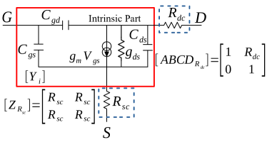
In contrast to previous works [19, 20, 21], the approach used here is based on linear matrices in order to remove the contribution of the contact resistances from the de-embedded parameters. As Fig. 3 shows, is connected in series with the intrinsic part , while is connected in a cascade topology.
Then, using the following equations, where the operator implies a matrix transformation, intrinsic admittance parameters can be obtained from de-embedded parameters.
| (17) |
| (18) |
| (19) |
| (20) |
3 Low- and high-frequency noise model for CNTFETs
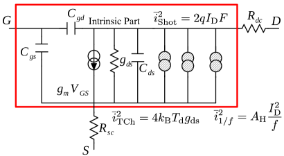
Four different noise sources have been considered in this work: thermal noise associated to resistive elements, shot channel noise due to the Schottky junctions, thermal channel noise associated to an equivalent noise temperature and flicker noise (1/), mostly present at low frequencies. Details related to each noise source are presented below.
3.1 Thermal noise in resistive elements
The thermal noise in resistive elements of the equivalent circuit, as a result of the movement of the free carriers inside the conductive material [28], can be described by its power spectral density as:
| (21) |
where is the Boltzmann constant, is the resistance, is the noise bandwidth, which is considered equal to one for all cases in this work and is the absolute temperature. Each resistance present in the equivalent circuit has a characteristic power spectral density to describe its produced thermal noise.
3.2 Shot channel noise
The carrier injection in CNTFETs will be affected as a consequence of the potential barriers in the channel [29, 30, 5]. The carrier injection through the potential barrier, when a low carrier density is present in the channel, follows a Poisson’s probability distribution. The result is a power spectral density associated to the shot noise represented in equation (22) where is the electron charge, is the drain current and the Fano Factor, which represents the compression of the shot noise as a result of the correlation between successive carriers injections in the potential barriers [31]. When no correlation exists is equal to one, as it has been considered in this work.
| (22) |
3.3 Thermal channel noise
The relaxed channel length (e.g., ) [32, 9, 1] and the large density of tubes in high-frequency CNTFETs, as well as the bias near saturation required for the dynamic performance of these devices, induce the activation of scattering mechanisms of acoustic and optical phonons, hence, non-ideal ballistic transport exists in these devices and the channel resistance can not be neglected [27]. As a result of this channel resistance, thermal channel noise spectral power density is considered as in the Pospieszalski model [33]. The corresponding expression, based on drift-diffusion theory and applied here to CNTFETs due to the transport conditions described above, is shown in equation (23).
| (23) |
An equivalent noise temperature (), associated to the output conductance, is needed to describe the thermal channel noise. Equation (24) describes the equivalent noise temperature [34], as it can be noticed, is independent to the frequency and only depends on the room temperature and the relation between and .
| (24) |
3.4 Flicker noise (1/)
Flicker noise presents an inversely proportional power spectral density as a function of the frequency. Previous studies refer that flicker noise is specially large in CNTFETs [30, 35, 36, 37] and it is related to the total number of charge carriers [35].
The power spectral density of the flicker noise is described in equation (25). In this equation represents the noise amplitude which scales the noise contribution and is equal to the relation between the Hooge’s constant (), dependent on the scattering channel mechanisms, and the number of charge carriers in the channel () [38]. On the other hand, is an empirical parameter which is commonly in the order between and for non-optimized materials [39] as is the CNTFETs case. For this work the chosen value was . Notice that a dominant mobility variation mechanism has been considered here to describe the flicker noise.
| (25) |
Once that all proposed noise sources are known these can be added to the electrical equivalent circuit as shows Fig. 4.
As it can be noticed, the considered noise model is related to the small-signal model presented before and as a result of that, accurate projections for dynamic and noise CNTFETs performance are only possible if all parameters are extracted appropriately. Thus, a correct extraction of contact resistance is mandatory in order to achieve a good approximation to CNTFETs performance.
4 Validation of the proposed model using a reference compact model
4.1 Initial reference data
The compact model used as a reference in this work [17, 18], which is called CCAM, has been originally calibrated to hysteresis-free experimental data from a CNTFET technology presented elsewhere [32]. Specifically, the top-gated device used as a reference for this work has a device channel length () of around and a gate length () of around . The device has eight gate fingers of each one forming a total device width () of approximately . The semiconducting-to-metallic (s:m) CNT ratio is 3:1 with around 3000 CNTs randomly distributed in channel and grown via chemical vapor deposition (CVD) on SiO2. Metallic contacts of the device are made from Pd/Ti. Details on the fabrication process can be found in [32].
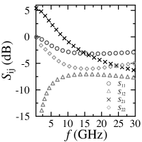
In order to perform the extraction of the associated equivalent circuit parameters, results obtained from the reference compact model have been used. The contribution of metallic tubes has been turned-off for this study in order to work with the best-case scenario. The bias point has been chosen at and since an optimal high-frequency performance has been found out for this technology under such conditions [12]. The transit frequency () and maximum oscillation frequency () obtained with the reference model for the considered DC bias point are and , respectively. By using CCAM, the -parameters of the device have been simulated from as shown in Fig. 5. These results have been used as the starting point to extract the parameters of the equivalent circuit (see Fig. 1) for this device by using the methodology presented in Section 2.
4.2 Parameters extraction results
In this case, the extrinsic parameters have been obtained directly from CCAM, where access resistances and inductances have been neglected, since pad-de-embedding data is used for the original calibration [17]. The extrinsic parameters are summarized in Table 1.
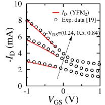
Regarding to the contact resistance extraction, Fig. 6 shows the transfer characteristics of the device simulated with the reference compact model. Red lines in Fig. 6 represent the drain current calculated with a drift-diffusion approach (see Eq. (3) in [27]) considering , extracted using YFM2.
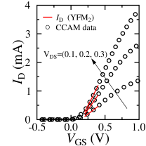
The device exhibit an -type behavior, i.e., carriers are injected from the source to the channel, which causes a larger impact of the potential barrier at the source on the device performance. Considering the latter, a distribution of the total contact resistance is proposed as follows: and . These values are confirmed by a fitting procedure involving the noise performance developed in Section 4.3.
Then intrinsic parameters have been extracted following the proposed procedure (see Section 2.4). Parameters of the extracted equivalent circuit are summarized in Table 1.
-
Parameter Extracted value Optimized value Intrinsic part () () () () () Contact resistance () () Extrinsic part () () () () () ()
*Extracted extrinsic parameters have been obtained directly from CCAM calibration data. Access resistances and inductances have been neglected during CCAM calibration process.
In order to demonstrate the feasibility of the extracted transconductance and output conductance, these have been compared with results from equations for traditional FETs considering a non-negligible contact resistance with no bias-dependence (equations (26) and (27)). Such equations have described properly different FET technologies, regardless the channel length, in saturation and linear regimes [40].
| (26) |
| (27) |
and can be obtained from de-embedded data (, see eq. (1)) using equations (13) and (14), respectively. In this case, as a result of the hysteresis-free data, and can also be obtained from DC curves. A comparison between extracted and calculated results of and shows that both results are equal, therefore both approaches to obtain these intrinsic parameters are valid.
Notice that the charge and current transport are described in this work by relations based on the admittance device parameters (see Eqs. (13) to (16)) in contrast to CCAM where such phenomena have been described by semi-empirical expressions. Hence, the approach presented here is expected to be more efficient for immediate characterization purposes.
4.3 Results and discussion
The corresponding simulation of the electrical equivalent circuit has been implemented using Keysight Advanced Design System (ADS) from the extracted values of the Table 1. The considered bias point is and resulting in .
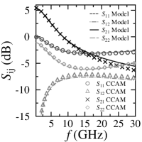
At frequencies up to , which is around , the performance of -parameters is similar for both CCAM and the extracted equivalent circuit. However, at frequencies higher than , the difference between results from CCAM and from the equivalent circuit increases (not shown here). Due to this difference, mainly caused by extrinsic parameters, an optimization has been performed in order to find a good agreement. The optimization procedure consists in minimizing the difference between dynamic and noise results from the proposed model and reference data by fitting only extrinsic parameters, this has been done using the optimization tools of ADS based on a least-squares error-function [41, 42]. Extracted and optimized parameters for the electrical equivalent circuit are compared in Table 1.
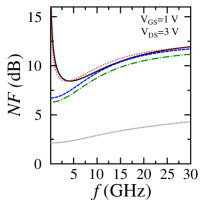
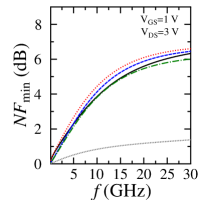
Table 1 shows that only two extrinsic parameters have changed as a result of the optimization process. A good agreement has been found for results from CCAM and from the proposed equivalent circuit for -parameters as well as for noise parameters (only and are shown here) when optimized values are considered as shown in Figs. 7(a) and 7(b). A correct distribution of the total contact resistance allows a good agreement of -parameters and noise results from equivalent circuit and from CCAM. From Fig. 7(b) it can be observed that a good agreement between equivalent circuit and CCAM has been found for frequencies commonly used for circuit design @: for the proposed model and while for CCAM and .
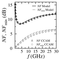
From noise results depicted in Fig. 8 it has been shown that shot noise mainly contributes to the total noise over all frequency range. This trend has been reported in [6, 30, 43], while flicker noise does at low frequencies, the same trend has been found in [30, 35, 37, 36].
5 Characterization of a fabricated device
The proposed methodology and model have been also applied to experimental data from a fabricated top-gated MT-CNTFET which is detailed in [19]. Extrinsic transit frequency () and extrinsic maximum oscillation frequency () obtained from measured -parameters are and , respectively. An intrinsic has been calculated for the device in [19]. The device has a gate length of and channel width of , its channel incorporates a large number of aligned SW-CNTs grown by CVD with a nanotube density of 5 and a s:m ratio of 3:1. Metallic contacts were made from Ti/Au by a photolithography process in a ground-signal-ground (GSG) configuration. The transistor has a -like behavior and the chosen bias point was and . Measurements on test “open” structures have been reported in [19].
Contact resistances have been extracted from transfer characteristics obtained using reported measured output characteristics [19]. It is important to notice that the value of contact resistance has not been reported and hysteresis has been neglected in [19]. Fig. 9 shows transfer characteristics of the device and the calculated with the YFM2 method [27]. The extracted value of contact resistance was and the contribution of each contact has been considered as identical, i.e., .
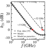
A comparison between the -parameters obtained from the proposed model and experimental data from [19] is shown in Fig. 10. A good agreement has been achieved using the proposed methodology and the optimizing process in which only four extrinsic parameters have been fitted. In contrast with the equivalent circuit in [19], whose parameters have been extracted only by fitting the data and no extrinsic parameters have been treated, in this work an extraction procedure for both the intrinsic and the extrinsic parameters along contact resistances, has been considered. Table 2 shows extracted values and a comparison with the equivalent circuit values in [19].


| Extracted | Optimized | Reported | |
| Parameter | value | value | value [19] |
| Intrinsic part | |||
| () | |||
| () | |||
| () | |||
| () | |||
| () | |||
| Contact resistance | |||
| () | - | ||
| () | - | ||
| Extrinsic part | |||
| () | |||
| () | |||
| () | |||
| () | - | - | - |
| () | - | ||
| () | - | - | - |
| () | - | ||
| () | - | - | - |
| () | - | ||
| () | |||
| () | |||
| () | |||
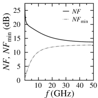
Moreover, the noise model provides the projection of the device noise performance as shown in Fig. 11(a). Experimental noise data reported in [6] for a device from the technology described in [32] indicates similar noise results. Both devices have been biased in the active transistor region. Reference [6] reported a measured at and the proposed model based on experimental data from [19] shows a at the same frequency. The noise performance improvement of [19] in comparison to experimental data from [6] can be related to different fabrication processes, e.g., the device reported in [6, 32] has a channel formed by misaligned CNTs, whereas the device in [19] has a channel formed by aligned CNTs.
In addition, Fig. 11(b) shows for both: experimental data from [19] and equivalent circuit. In both cases the cut-off frequency is close to . Studies considering only the intrinsic part and the contact resistances of the device, i.e., without extrinsic parameters, have been made and the corresponding results can be observed in Fig. 11(b). As it is mentioned in [19] the intrinsic cut-off frequency is close to . In contrast to the equivalent circuit proposed in [19] in this work the intrinsic part of the equivalent circuit can reproduce the projected free-parasitic performance.
6 Conclusions
An equivalent circuit to model the low- and high-frequency dynamic and noise performance of CNTFETs has been proposed. The equivalent circuit allows the immediate and efficient evaluation of the performance for CNTFETs considering the effect of the contact resistance as well as extrinsic and intrinsic parameters. The proposed strategy includes the accurate extraction of the total contact resistance and a methodology to remove their contribution to the intrinsic part of the equivalent circuit. Moreover, we have shown that, noise data can be useful to perform an accurately distribution of the total contact resistance. Furthermore, a comparison of the extracted and values from the proposed strategy was carried out with values from an extraction methodology for large contact resistance classic FET [40] and similar results have been found.
The proposed approach has been applied to two different technologies. In the former case, after the optimization process only two parasitic parameters have changed. Considering the optimized values a close behavior has been found between results from the reference compact model (CCAM) and results from the proposed equivalent circuit for -parameters and noise figures of merit. In the second case, the methodology has been applied to experimental data from a top-gated CNTFET [19], in this case a good agreement between model and experimental data has been found for -parameters after the optimization process in which only four extrinsic parameters have changed. Moreover, noise performance has been simulated giving insights about the expected performance of the device. The intrinsic part of the proposed equivalent circuit for this technology is also able to reproduce closely the expected performance of the device if parasitics were not considered.
Finally, the proposed methodology can be applied to other emergent technologies with large contact resistance because this approach properly considers the effect of the contact resistance in device performance. Moreover a procedure to obtain and remove its contribution in order to extract accurately the intrinsic part of the equivalent circuit has been provided.
References
References
- [1] Marsh PF, Rutherglen C, Kane AA, Cain TA, Galatsis K, Maas S, AlShareef MR 2019 Solving the Linearity and Power Conundrum: Carbon Nanotube RF Amplifiers, Microwave Journal, 62, 22-32.
- [2] Baumgardner JE, Pesetski AA, Murduck JM, Przybysz JX, Adam JD, Zhang H 2007 Inherent linearity in carbon nanotube field-effect transistors Applied Physics Letters, 91 052107.
- [3] Mothes S, Claus M, Schröter M 2015 Toward Linearity in Schottky Barrier CNTFETs, IEEE Transactions on Nanotechnology, 14, 372-378.
- [4] Maas S 2017 Linearity and Dynamic Range of Carbon Nanotube Field-Effect Transistors Proc. IEEE MTT-S International Microwave Symposium (Honololu), (IEEE Inc.), p 87-90.
- [5] Landauer GM and Gonzalez JL 2014 Radio-Frequency Performance of Carbon Nanotube-Based Devices and Circuits Considering Noise and Process Variation IEEE T. on Nanotechnology, 13, 228-237.
- [6] Sakalas P, Schröter M, Bölter M, Claus M, Mothes S and Wang D 2011 High frequency noise in manufacturable carbon nanotube transistors Proc. 21st International Conference on Noise and Fluctuations (Toronto) (IEEE Inc.), p 372-5.
- [7] Hasan S, Salahuddin S, Vaidyanathan M and Alam MA 2006 High-frequency performance projections for ballistic carbon-nanotube transistors IEEE T. on Nanotechnology 5 14-22.
- [8] Guo J, Hasan S, Javey A, Bosman G and Lundstrom M 2005 Assessment of high-frequency performance potential of carbon nanotube transistors, IEEE T. on Nanotechnology 4 715-21.
- [9] Cao Y, Brady GJ, Gui H, Rutherglen C, Arnold MS, Zhou C 2016 Radio Frequency Transistors Using Aligned Semiconducting Carbon Nanotubes with Current-Gain Cutoff Frequency and Maximum Oscillation Frequency Simultaneously Greater than 70 GHz ACS Nano 10 6782-90.
- [10] C. Rutherglen et al. 2019 Wafer-scalable, aligned carbon nanotube transistors operating at frequencies of over 100 GHz Nature Electronics 2 530-539.
- [11] D. Zhong et al. 2019 Carbon Nanotube Film-Based Radio Frequency Transistors with Maximum Oscillation Frequency above 100 GHz ACS Applied Materials & Interfaces 11 45.
- [12] Ramos-Silva JN, Pacheco-Sanchez A, Diaz-Albarran LM, Rodriguez-Mendez LM, Schröter M and Ramirez-Garcia E 2019 High-frequency performance study of CNTFET-based amplifiers, submitted to IEEE Transactions on Nanotechnology.
- [13] Schröter M, Claus M, Sakalas P, Haferlach M, Wang D 2013 Carbon nanotube FET technology for radio-frequency electronics: state-of-the art overview IEEE J. of the Electron Devices Society 1 9-20.
- [14] Eron M, Lin S, Wang D, Schöter M, Kempf P 2011 L-band carbon nanotube transistor amplifier, Electronics Letters 47 265-6.
- [15] Taghavi A, Carta C, Ellinger F, Haferlach M, Claus M, Schöter M 2015 A CNTFET Amplifier with 5.6 dB Gain Operating at 460-590 MHz Proc. SBMO/IEEE MTT-S International Microwave and Optoelectronics Conference (Porto de Galinhas) (IEEE Inc.) p 1-4.
- [16] Svensson J, Campbell EB 2011 Schottky barriers in carbon nanotube metal-contacts J. of Appl. Phys. 110 111101.
- [17] Schröter M, Haferlach M, Pacheco-Sanchez A, Mothes S, Sakalas P and Claus M 2015 A semiphysical large-signal compact carbon nanotube FET model for analog RF applications, IEEE Trans. on Electron Dev. 62 52-60.
- [18] Schröter M, Haferlach M and Claus M 2015 CCAM Compact Carbon Nanotube Field-Effect Transistor Model 2015 NanoHUB http://dx.doi.org/10.4231/D34F1MK28.
- [19] Kocabas C et al. 2009 High-Frequency Performance of Submicrometer Transistors That Use Aligned Arrays of Single-Walled Carbon Nanotubes Nano Lett. 9 1937-43.
- [20] Marani R, Gelao G, Soldano P and Perri AG 2015 An Active CNTFET Model for RF Characterization Deduced from S Parameters Measurements Current Nanoscience 11, 36-40.
- [21] M. Tuo et al. 2017 Suspended individual SWCNT characterization via bottom gate FET configuration Microwave and Optical Technology Letters 59 10 2610-2614.
- [22] Aaron D. Franklin, Damon B. Farmer, and Wilfried Haensch 2014 Defining and Overcoming the Contact Resistance Challenge in Scaled Carbon Nanotube Transistors ACS Nano 8 7333-7339.
- [23] Qing Cao et al. 2012 Evaluation of Field-Effect Mobility and Contact Resistance of Transistors That Use Solution-Processed Single-Walled Carbon Nanotubes ACS Nano 6 6471-6477.
- [24] Tiemeijer LF, Havens RJ, Jansman ABM and Bouttement Y 2005 Comparison of the ”pad-open-short” and ”open-short-load” de-embedding techniques for accurate on-wafer RF characterization of high-quality passives IEEE T. on Microwave Theory and Techniques 53 723-9.
- [25] Tiemeijer LF and Havens RJ A calibrated lumped-element de-embedding technique for on-wafer RF characterization of high-quality inductors and high-speed transistors IEEE T. on Electron Dev. 50 822-9.
- [26] M. C. A. M. Koolen, J. A. M. Geelen, and M. P. J. G. Versleijen 1991 An improved de-embedding technique for on-wafer high frequency characterization Proc. IEEE Bipolar/BiCMOS Circuits Technology Meeting (IEEE Inc.) p 188-191.
- [27] Pacheco-Sanchez A, Claus M, Mothes S and Schröter M 2016 Contact resistance extraction methods for short- and long-channel carbon nanotube field-effect transistors Solid-State Electronics 125 161-6.
- [28] van Der Ziel A 1986 Noise in Solid State Devices and Circuits (New York, NY:Wiley).
- [29] Navid R, Jungemann C, Lee TH and Dutton RW 2007 High-frequency noise in nanoscale metal oxide semiconductor field effect transistors, J. of Appl. Phys. 101 124501.
- [30] Landauer GM and Gonzalez JL 2012 A compact noise model for carbon nanotube FETs, Proc. International Semiconductor Conference Dresden-Grenoble (Grenoble) (IEEE Inc.) p 53-6.
- [31] Betti A, Fiori G and Iannaccone G 2009 Shot Noise Suppression in Quasi-One-Dimensional Field-Effect Transistors, IEEE T. on Electron Dev. 56 2137-43.
- [32] Schröter M, Kolev P, Wang D, Eron M, Lin S, Samarakone N, Bronikowski M, Yu Z, Sampat P, Syams P, McKernan S 2011 A 4” Wafer Photostepper-Based Carbon Nanotube FET Technology for RF Applications 2011 IEEE MTT-S International Microwave Symposium (Baltimore) (IEEE Inc.) 5972750.
- [33] Pospieszalski MW 1989 Modeling of Noise Parameters of MESFETs and MODFETs and Their Frequency and Temperature Dependence IEEE T. on Microwave Theory and Techniques, 37 1340-50.
- [34] Aguilar ME, Crozat P, Hackbarth T, Herzog HJ and Aniel F 2005 Microwave noise performance and modeling of SiGe-based HFETs, IEEE T. on Electron Dev. 52 2409-15.
- [35] Lin YM, Appenzeller J, Knoch J, Chen Z and Avouris P 2006 Low-Frequency Current Fluctuations in Individual Semiconducting Single-Wall Carbon Nanotubes Nano Lett. 6 930-6.
- [36] Collins PG, Fuhrer MS and Zettl A 2000 1/f noise in carbon nanotubes, Appl. Phys. Lett. 76 894-96.
- [37] Appenzeller J, Lin Y, Knoch J, Chen Z and Avouris P 2007 1/f Noise in Carbon Nanotube Devices-On the Impact of Contacts and Device Geometry IEEE T. on Nanotechnology 6 368-73.
- [38] Hooge FN 1969 1/f noise is no surface effect, Phys. Lett. 29A 139-40.
- [39] Hooge FN 1994 1/f noise sources IEEE T. on Electron Dev. 41 1926-35.
- [40] Chou SY and Antoniadis DA 1987 Relationship between measured and intrinsic transconductances of FET’s IEEE Trans. on Electron Dev. 34 448-50.
- [41] S.E. Laux 1985 Techniques for Small-Signal Analysis of Semiconductor Devices IEEE Trans. on Electr. Dev. 32 2028-37.
- [42] J.P. Roux, L. Escotte, R. Plana and J. Graffeuil 1995 Small-Signal and Noise Model Extraction Technique for Heterojunction Bipolar Transistor at Microwave Frequencies IEEE T. on Microw. Theory and Techn. 43 293-298.
- [43] Marani R, Gelao G and Perri AG 2017 A Compact Noise Model for C-CNTFETs, ECS J. of Solid State Science and Technology 6 M44-9.