Detection of the Orbital Hall Effect by the Orbital-Spin Conversion
Abstract
The intrinsic orbital Hall effect (OHE), the orbital counterpart of the spin Hall effect, was predicted and studied theoretically for more than one decade, yet to be observed in experiments. Here we propose a strategy to convert the orbital current in OHE to the spin current via the spin-orbit coupling from the contact. Furthermore, we find that OHE can induce large nonreciprocal magnetoresistance when employing the magnetic contact. Both the generated spin current and the orbital Hall magnetoresistance can be applied to probe the OHE in experiments and design orbitronic devices.
I Introduction
The intrinsic orbital Hall effect (OHE), where an electric field induces a transverse orbital current, was proposed by the Zhang group Bernevig et al. (2005) soon after the prediction of the intrinsic spin Hall effect (SHE) Murakami et al. (2003); Sinova et al. (2004). The SHE was soon observed Kato et al. (2004); Wunderlich et al. (2005), later applied for the spintronic devices(Jungwirth et al., 2012, and references therein), and also led to the seminal discovery of the quantum SHE, i.e., the 2D topological insulator Kane and Mele (2005); Bernevig et al. (2006). Different from the SHE, the OHE does not rely on the spin-orbit coupling (SOC), and thus, it was predicted to exist in many materials Bernevig et al. (2005); Guo et al. (2005); Kontani et al. (2008a, b); Tanaka et al. (2008); Tokatly (2010); Go et al. (2018); Jo et al. (2018); Phong et al. (2019); Canonico et al. (2020); Bhowal and Satpathy (2020) with either weak or strong SOC, for example, in metals Al, Cu, Au, and Pt.
In an OHE device, the transverse orbital current leads to the orbital accumulation at transverse edges, similar to the spin accumulation in a SHE device. Zhang et al Bernevig et al. (2005) proposed to measure the edge orbital accumulation by the Kerr effect. Recently, Ref. Go and Lee, 2020 predicted the orbital torque generated by the orbital current. However, the OHE is yet to be detected in experiments until today. The detection of the orbital is rather challenging, because the orbital is highly non-conserved compared to the spin, especially at the device boundary.
A very recent work by us proposed Liu et al. (2020) that the longitudinal current through DNA-type chiral materials is orbital-polarized, and contacting DNA to a large-SOC material can transform the orbital current into the spin current. Thus, we are inspired to conceive a similar way to detect the transverse OHE by converting the orbital to the spin by the SOC proximity.
In this article, we propose two ways to probe the OHE, where the strong SOC from the contact transforms the orbitronic problem to the spintronic measurement. One way is to generate spin current or spin polarization from the transverse orbital current by connecting the edge to a third lead with the strong interfacial SOC. Then the edge spin polarization and spin current is promising to be measured by the Kerr effect Kato et al. (2004) and the inverse SHE Saitoh et al. (2006); Valenzuela and Tinkham (2006); Zhao et al. (2006), respectively. The other way is to introduce a third magnetic lead and measure the magnetoresistance. We call it the orbital Hall magnetoresistance (OHMR), similar to the spin Hall magnetoresistance Huang et al. (2012); Weiler et al. (2012). In our proposal, the OHE refers to orbitals that resemble atomic-like orbitals, which naturally couple to the spin via the atomic SOC. We first demonstrate detection principles in a lattice model by transport calculations. Then we incorporate these principles into the metal copper, which has negligible SOC and avoids the co-existence of the SHE, as a typical example of realistic materials. In the copper based device, we demonstrate the resultant spin polarization/current and very large OHMR (), which are measurable by present experiment techniques.
II Results and Discussions
II.1 Methods and General Scenario
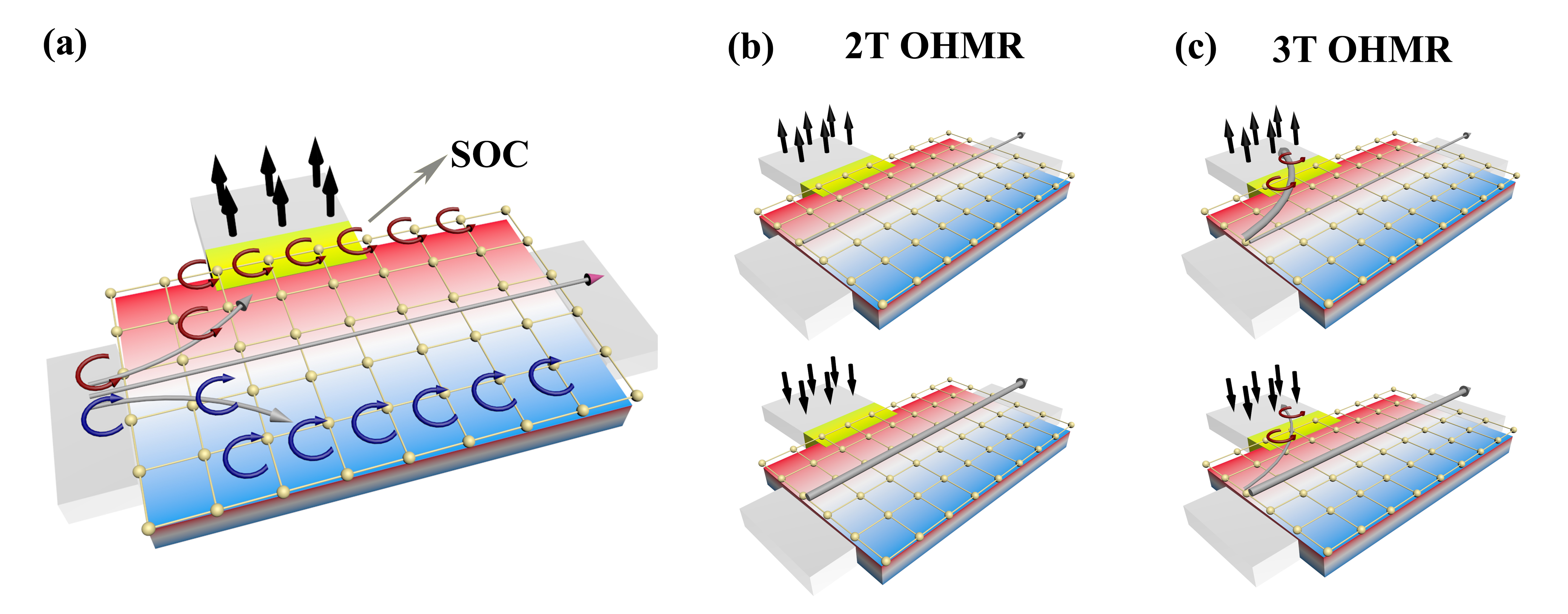
To detect the OHE, we introduce an extra contact with the strong SOC on the boundary of the OHE material, as shown in Figure 1. This device can act for both two-terminal (2T) and three-terminal (3T) measurements (or more terminals). In theoretical calculations, we completely exclude SOC from all leads so that we can well define the spin current. We also remove SOC in the OHE material, the device regime in the center, to avoid the existence of SHE. Only finite atomic SOC is placed in the interfacial region (highlighted by yellow in Figure 1) between the OHE and the third lead.
We first prove the principle by a simple square-lattice model that hosts OHE. As shown in the inset of Figure 2(a), a tight-binding spinless model is constructed, with three orbitals , and assigned to each site. Under the above basis, the atomic orbital angular momentum operator is written as
| (1) |
And three eigenstates correspond to eigenvalues , respectively. After considering the nearest neighboring hopping, the Hamiltonian is written as
| (2) |
where , and are onsite energies of , and orbitals. , , , are electron hopping integrals between orbitals, type oriented orbitals, type oriented orbitals, and and orbitals, respectively. In the following calculations, their values are specified as , , , , , and , in the unit of eV. To realize the OHE, it requires the inter-orbital hopping to induce the transverse current. Since and orbital are orthogonal under the square lattice geometry, the inter-orbital hopping becomes the critical parameter that controls the existence of the OHE. Then we introduce the atomic SOC on the boundary to demonstrate the OHE detection by , where is the spin operator.
We estimate the OHE conductivity () with the orbital Berry curvature in the Kubo formula Xiao et al. (2010); Nagaosa et al. (2010),
| (3) |
| (4) |
where is the “orbital” Berry curvature for the band with Bloch state and energy eigenvalue . is the Fermi-Dirac distribution function. is the component of the band velocity operator while is the orbital current operator in the direction, defined as . Therefore, the above formula indicates that the interband perturbation induces the orbital Berry curvature, further reiterating the importance of inter-orbital hopping. We also note that, the orbital Berry curvature is even under the time-reversal symmetry or the spatial inversion symmetry, .
For the device schematically presented in Figure 1, we calculated the conductance by the Landauer-Büttiker formula Büttiker (1986) with the scattering matrix from lead to lead ,
| (5) |
where is the scattering matrix element from the -th eigenstate in lead to the eigenstate in lead . In all three leads (), spin () is a conserved quantity because of the lack of SOC. We turn off the inter-orbital hopping in leads so that is also conserved, i.e., commutes with the Hamiltonian (See Supplementary Materials). Therefore, with the spin and orbital conserved leads, we can specify the conductance in each and channel, and define the orbital- and spin-polarized conductance as:
| (6) | ||||
| (7) |
where is the conductance from lead to the channel of lead . is omitted here since contributes no polarization. We performed the conductance calculations with the quantum transport package Kwant Groth et al. (2014).
As illustrated in Figure 1(a), electrons with the opposite orbital angular momentum deflect into transverse directions in the OHE region, resulting in the transverse orbital current. Therefore, orbital accumulates at two sides, and the orbital polarization emerges. To detect the orbital polarization, atomic SOC is added at one side, as highlighted by yellow in Figure 1(a). After electron deflecting into the SOC region, the right-handed orbital (red circular arrows) is converted to the up spin polarization. If a third lead is further attached, the SOC region converts the orbital current into the spin current. If the third lead exhibits magnetization along () (Figure 1(b) and 1(c)), inversely, the OHE induces the OHMR, relying on whether is parallel or anti-parallel to the generated spin polarization. In the 2T measurement (Figure 1(b)), the conductance from lead 1 to lead 2 () changes when the direction is reversed. And the changing direction of depends sensitively on the size of the device, due to the complex orbital accumulation and reflection with an open lead. While for its spin counterpart, the SHE-induced magnetoresistance is commonly measured in a 2T setup Huang et al. (2012); Weiler et al. (2012). In the 3T device (Figure 1(c)), the situation is simpler since the transverse orbital current can flow into the third lead. If and spin polarization is parallel (anti-parallel), the transverse orbital current matches (mismatches) the lead magnetization, resulting in the high (low) and low (high) accordingly. We point out that the 3T measurement is usually more favorable than 2T, since the 3T device avoids the 2T reciprocity constrain Büttiker (1988) and the conductance change [] is also relatively larger in the third lead, as discussed in the following.
II.2 Spin Polarization and Spin Current Generated by the OHE
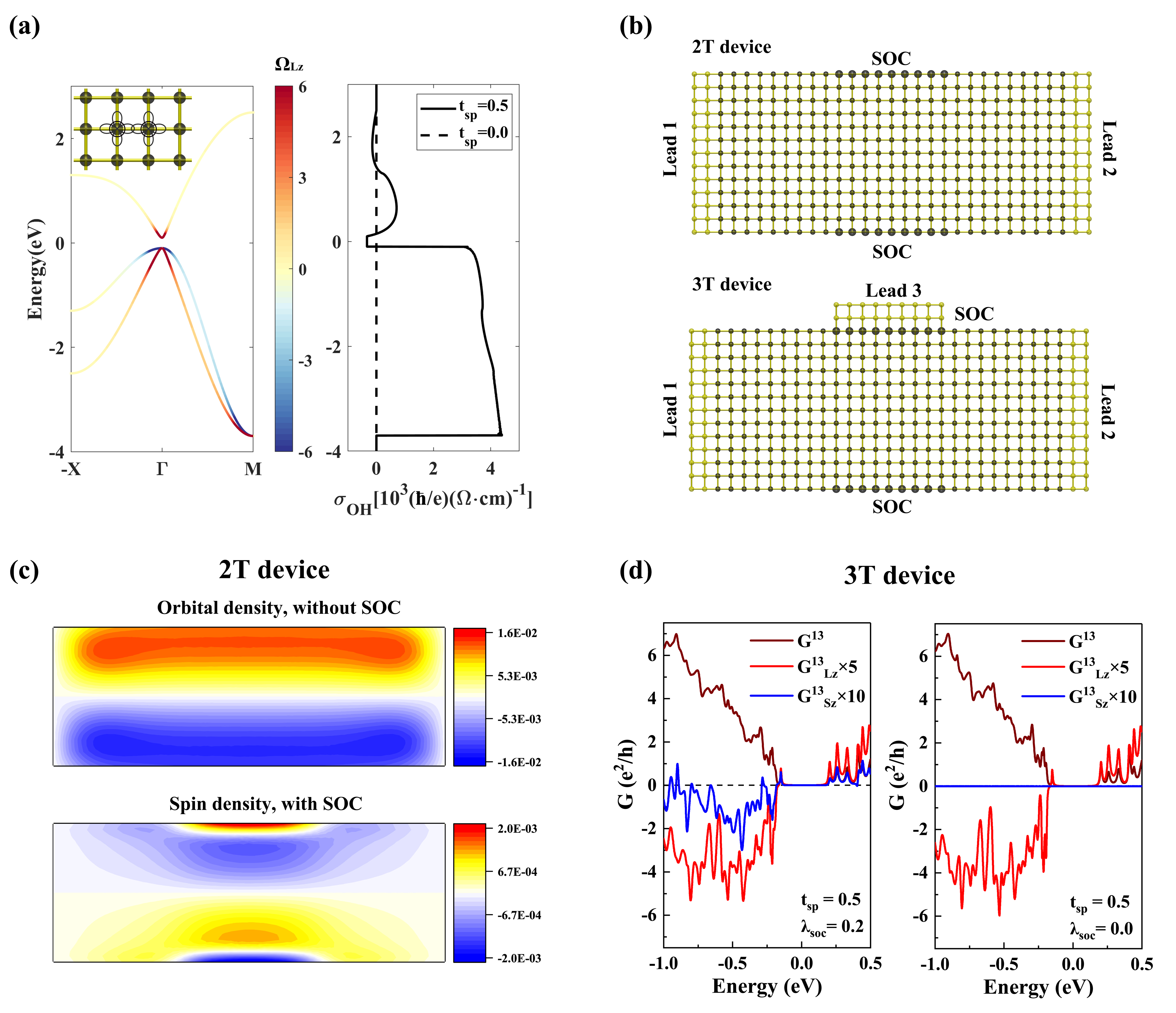
The band structure weighted by the orbital Berry curvature for the square lattice is plotted in Figure 2(a). The highest band corresponds to the orbital dispersion, while two lower bands are dominated by orbitals. The orbital Berry Curvature concentrates near the point, point and - line in the Brillouin zone, where band hybridization is strong. After integrating in the Brillouin zone, the orbital Hall conductivity is derived and presented in Figure 2(a). It shows that, due to the inter-orbital hopping , states below ( orbitals) and above ( orbital) Fermi level both exhibits significant . However, if is turned off so that is conserved, both and vanishes.
Based on the square lattice with finite , the 2T device is constructed, as shown in Figure 2(b). Without SOC at two sides, the orbital density distribution is plotted in Figure 2(c), which shows that opposite orbitals accumulate and polarize at two boundaries. With SOC turned on, spin density appears and largely concentrates on the local SOC atoms, which is promising to be detected by the Kerr effect Kato et al. (2004). Since SOC couples the () orbital to the () spin and forms the () state, the spin density near the SOC region largely follows the orbital density pattern: positive at the upper side and negative at the lower side. To verify that the spin polarization is directly induced by the OHE rather than SOC, we turned off the OHE by setting eV and preserve the SOC at the interface. The supplementary Figure S2 shows that both the orbital and spin polarization disappear.
On the basis of 2T device, a third lead is attached to the SOC side to form a 3T device, as shown in Figure 2(b). Therefore, rather than the orbital accumulation, the orbital current will flow into the third lead and generate the spin current. Figure 2(d) shows that the orbital current from lead 1 to lead 3 () exists with and without SOC at the interface. For instance, for states above Fermi level, states are more easily transported into lead 3 than states, and thus polarizes the lead, being consistent with the positive orbital polarization at the upper side in Figure 2(c). On the other hand, for the spin conductance, it only appears when turning on SOC, and the energy dependence of largely follows the orbital conductance, further demonstrating the spin generation process from the orbital. If we increase the SOC strength, increases accordingly, because of the higher orbital-spin conversion efficiency (see Figure S3). We also test orbital non-conserved leads with nonzero , whose spin conductance remains the similar feature (see Figure S4).
II.3 Orbital Hall Magnetoresistance
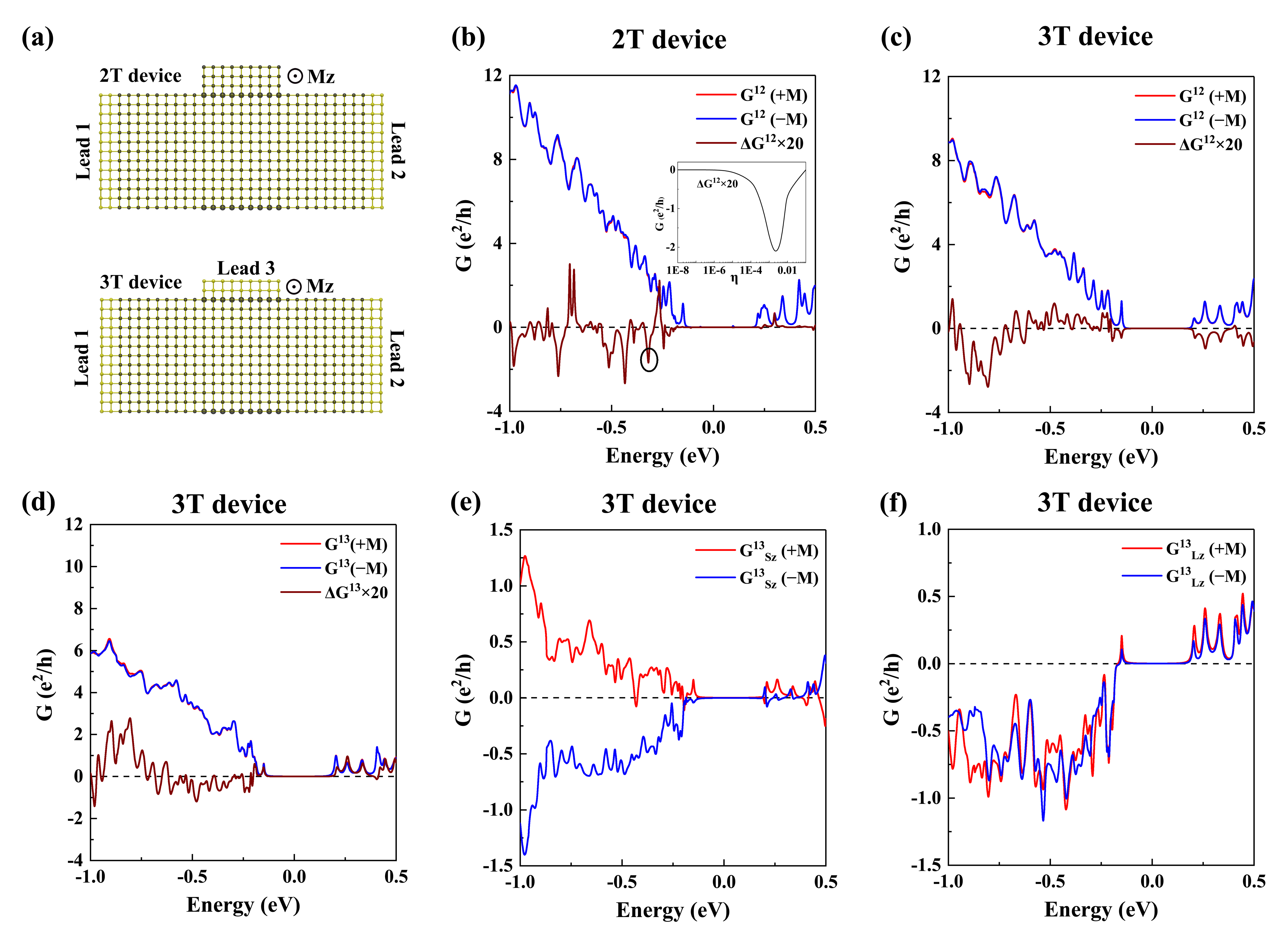
As discussed above, the current injected into lead 3 is spin-polarized. When lead 3 is magnetized along the axis, we expect the existence of magnetization-dependent conductance, i.e. . From the current conservation Büttiker (1988), we deduce the relation,
| (8) |
where . To demonstrate this, is introduced to lead 3 as an exchange field to the spin, as shown in the 3T setup in Figure 3(a). Results in Figure 3(c) and 3(d) indicate that and can reach several percentage of the total conductance at some energies. We also confirm that and are proportional to the exchange field strength (see Figure S5).
To understand the orbital induced magnetoresistance, the spin and orbital conductance from lead 1 to lead 3 are calculated. As shown in Figure 3(e), almost changes its sign when flipping in lead 3, as expected. And now inversely affects because of the interfacial SOC. When further comparing Figure 3(d) and 3(f), we found that the change of the magnitude of is proportional to the change of total conductance . Therefore, it verifies the scenario in Figure 1(c): when the orbital matches the spin in magnetic leads, and thus is higher while is accordingly lower. Thus, it indicates the essential role of the orbital in connecting charge and spin in the transport.
However, the 2T results exhibit qualitatively different features from the 3T results. According to the reciprocity relation Büttiker (1988), the 2T conductance obeys . Only when the current conservation is broken, one may obtain the 2T magentoresistance. Therefore, we introduce a dephasing term to leak electrons into virtual leads Büttiker (1986) to release the above constrain. As shown in the inset of Figure 3(b), the is zero at , first increases quickly and soon decreases as further increasing . In the large limit, the system is totally out of coherence and thus, the conductance cannot remember the spin and orbital information. We note that the dephasing exists ubiquitously in experiments due to the dissipative scattering for example by electron-phonon interaction and impurities.
For the same , the 2T (Figure (3b)) roughly exhibits the opposite sign compared to the 3T (Figure (3c)) in the energy window investigated. Unlike that follows the change of (Figure (3f)), the change direction of depends on the geometry of the 2T device (see Figure S6). The magnitude of the 2T also depends sensitively on the value of . Its peak value (Figure (3b)), with around 0.001, is comparable with the 3T value in the same parameter regime. However, the 3T conductance avoids the strict constrain of the 2T reciprocity, and the existence of 3T OHMR does not rely on the dephasing. Furthermore, in the 3T setup, the magnetoresistance ratio in the third lead is also larger than , because of the lower total conductance of . Therefore, we propose that the 3T setup may be more advantageous to detect the OHE.
II.4 Realistic Material Cu
Based on the simple square lattice model, we demonstrate two main phenomena, the OHE-induced spin polarization / spin current current assisted by the atomic SOC on the boundary and the existence of OHMR. We further examine them in a realistic material Cu. This light noble metal is predicted to exhibit the strong OHE.
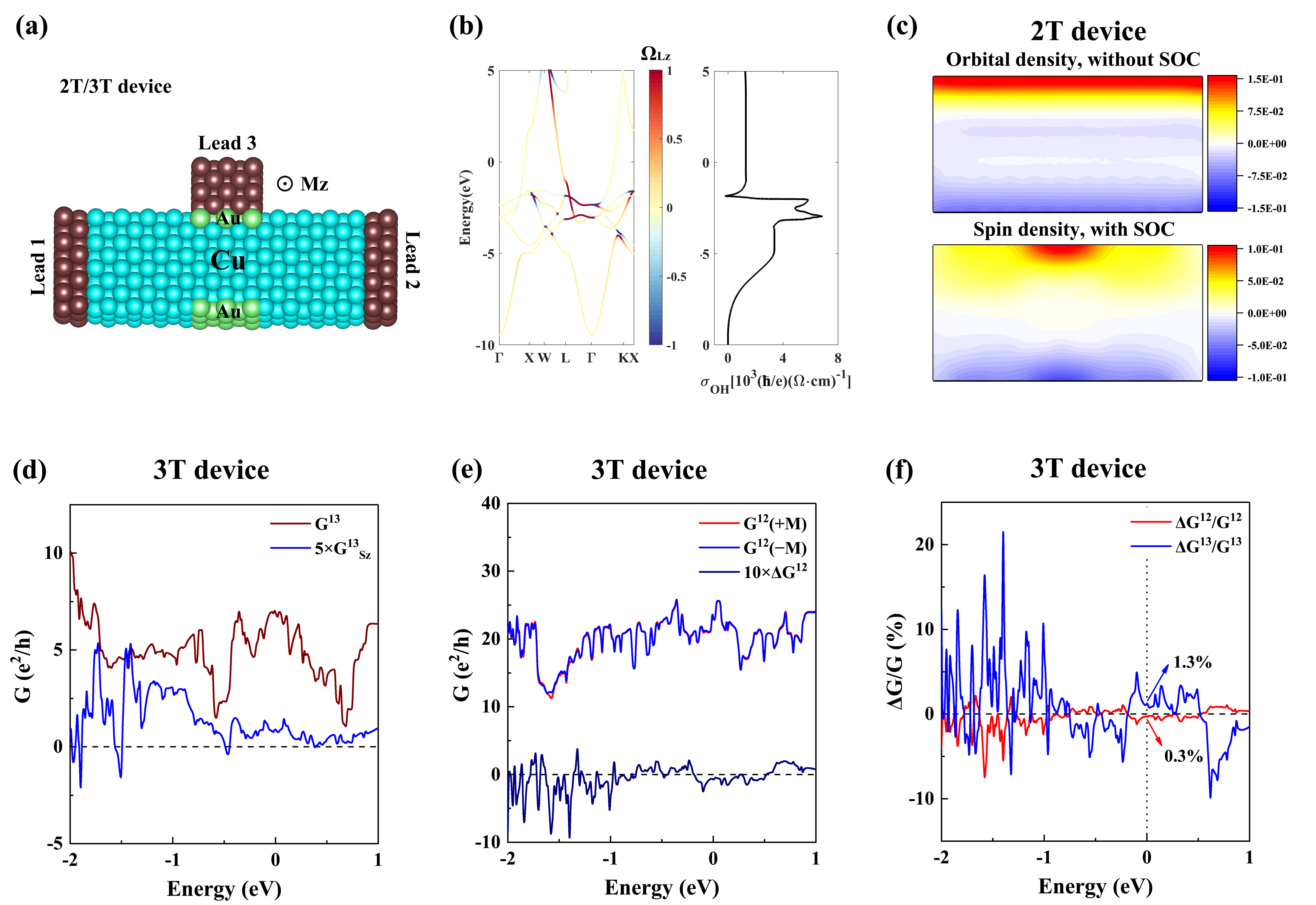
As shown in Figure 4(a), the 2T (without lead 3) and 3T devices are composed of Cu (without SOC) in both the scattering region and leads, and the heavy metal Au (with SOC) at two boundaries. We adopted the tight-binding method to describe the Cu and leads, where 9 atomic orbitals (, , , , , , , , ) are assigned to each site. The nearest-neighboring and the second-nearest-neighboring hoppings are considered with the Slater-Koster type parameters from Ref. Papaconstantopoulos et al., 1986. For the heavy metal Au at two sides, the SOC strength is set to 0.37 eV as suggested by Ref. Papaconstantopoulos et al., 1986. With the tight-binding approach, the first-principles band structure of Cu is reproduced (see Figure S7).
As shown in Figure 4(b), the orbital Berry curvature concentrates on the orbital region ( eV eV) due to the orbital hybridization, consistent with previous works Tanaka et al. (2008); Jo et al. (2018). After integrating , Figure 4(b) shows that the orbital Hall conductivity is around 6000 in the orbital region, even larger than the spin Hall conductivity of Pt. Near the Fermi level, the orbital Hall conductivity is determined by the -orbital derived bands and reduces to around 1000 .
For the 2T device, the orbital and spin density at Fermi level are plotted in Figure 4(c). The orbital polarization exists at two sides as a consequence of the OHE. With the heavy metal Au attached, spin polarization is generated, which concentrates on Au atoms and follows the orbital density pattern. To confirm that the spin polarization is induced by the OHE, we artificially turn off the inter-orbital hopping in Cu to eliminate the OHE, but still keep the SOC in the Au region. Result show that both the orbital and spin polarization disappear (see Figure S8), in accordance with our prediction.
For the 3T device, we add a third Cu lead to one SOC side and calculate the spin conductance from lead 1 to lead 3 (). As shown in Figure 4(d), the generated spin conductance displays an energy-dependence similar to the bulk . Near the Fermi level, the spin polarization rate can reach 4 , and it is even around 20 in the orbital region. Therefore, a sizable spin current can also be generated from the OHE by adding an interfacial SOC layer. Similarly, when artificially switching off the OHE of Cu but keeping the Au part, the spin current disappears, eliminating the contribution of the SHE brought by the thin Au layer (see Figure S9).
We also studied the OHMR by applying an exchange field in the lead 3. We choose eV according to the approximate spin splitting in the transition metal Co (see Figure S10). As shown in Figure 4(e) and 4(f), the 3T OHMR is rather large, where we find and at the Fermi level. In experiment, the SHE magentoresistance is around (see Ref. Avci et al., 2015 for example). Therefore, the sizable OHMR in copper can be fairly measurable by present experimental techniques. We should point out that similar effects can be generalized to other OHE materials like Li and Al Jo et al. (2018).
III Summary
In summary, we have proposed the OHE detection strategies by converting the orbital to spin by the interfacial SOC, and inducing the strong spin current/polarization. Inversely, the OHE can also generate the large nonreciprocal magnetoresistance when employing the magnetic contact. We point out that, compared to the two-terminal one, the three-terminal OHMR does not require the dephasing term , and may be more advantageous to detect the OHE. Using the device setup based on the metal Cu, we demonstrate that the generated spin polarization and OHMR are strong enough to be measured in the present experimental condition. Our work will pave a way to realize the OHE in experiment, and further design orbitronic or even orbitothermal devices for future applications.
IV Acknowledgement
We honor the memory of Prof. Shoucheng Zhang. This article follows his earlier works on the intrinsic orbital Hall effect and spin Hall effect. B.Y. acknowledges the financial support by the Willner Family Leadership Institute for the Weizmann Institute of Science, the Benoziyo Endowment Fund for the Advancement of Science, Ruth and Herman Albert Scholars Program for New Scientists, and the European Research Council (ERC) under the European Union’s Horizon 2020 research and innovation programme (Grant No. 815869, NonlinearTopo).
References
- Bernevig et al. (2005) B. A. Bernevig, T. L. Hughes, and S.-C. Zhang, Physical Review Letters 95, 066601 (2005).
- Murakami et al. (2003) S. Murakami, N. Nagaosa, and S.-C. Zhang, Science 301, 1348 (2003).
- Sinova et al. (2004) J. Sinova, D. Culcer, Q. Niu, N. Sinitsyn, T. Jungwirth, and A. H. MacDonald, Physical review letters 92, 126603 (2004).
- Kato et al. (2004) Y. K. Kato, R. C. Myers, A. C. Gossard, and D. D. Awschalom, science 306, 1910 (2004).
- Wunderlich et al. (2005) J. Wunderlich, B. Kaestner, J. Sinova, and T. Jungwirth, Physical review letters 94, 047204 (2005).
- Jungwirth et al. (2012) T. Jungwirth, J. Wunderlich, and K. Olejník, Nature materials 11, 382 (2012).
- Kane and Mele (2005) C. L. Kane and E. J. Mele, Physical review letters 95, 226801 (2005).
- Bernevig et al. (2006) B. A. Bernevig, T. L. Hughes, and S.-C. Zhang, science 314, 1757 (2006).
- Guo et al. (2005) G. Y. Guo, Y. Yao, and Q. Niu, Phys. Rev. Lett. 94, 226601 (2005).
- Kontani et al. (2008a) H. Kontani, T. Tanaka, D. S. Hirashima, K. Yamada, and J. Inoue, Physical Review Letters 100, 096601 (2008a), cond-mat/0702447 .
- Kontani et al. (2008b) H. Kontani, T. Tanaka, D. S. Hirashima, K. Yamada, and J. Inoue, Physical Review Letters 102, 016601 (2008b), 0806.0210 .
- Tanaka et al. (2008) T. Tanaka, H. Kontani, M. Naito, T. Naito, D. S. Hirashima, K. Yamada, and J. Inoue, Physical Review B 77 (2008), 10.1103/physrevb.77.165117.
- Tokatly (2010) I. V. Tokatly, Physical Review B 82, 161404 (2010), 1004.0624 .
- Go et al. (2018) D. Go, D. Jo, C. Kim, and H.-W. Lee, Physical Review Letters 121, 086602 (2018).
- Jo et al. (2018) D. Jo, D. Go, and H.-W. Lee, Phys. Rev. B 98, 214405 (2018).
- Phong et al. (2019) V. T. Phong, Z. Addison, S. Ahn, H. Min, R. Agarwal, and E. J. Mele, Phys. Rev. Lett. 123, 236403 (2019).
- Canonico et al. (2020) L. M. Canonico, T. P. Cysne, A. Molina-Sanchez, R. Muniz, and T. G. Rappoport, arXiv preprint arXiv:2001.03592 (2020).
- Bhowal and Satpathy (2020) S. Bhowal and S. Satpathy, Phys. Rev. B 101, 121112 (2020).
- Go and Lee (2020) D. Go and H.-W. Lee, Physical Review Research 2, 013177 (2020).
- Liu et al. (2020) Y. Liu, J. Xiao, J. Koo, and B. Yan, arXiv:2008.08881 (2020).
- Saitoh et al. (2006) E. Saitoh, M. Ueda, H. Miyajima, and G. Tatara, Applied physics letters 88, 182509 (2006).
- Valenzuela and Tinkham (2006) S. O. Valenzuela and M. Tinkham, Nature 442, 176 (2006).
- Zhao et al. (2006) H. Zhao, E. J. Loren, H. M. van Driel, and A. L. Smirl, Phys. Rev. Lett. 96, 246601 (2006).
- Huang et al. (2012) S. Y. Huang, X. Fan, D. Qu, Y. P. Chen, W. G. Wang, J. Wu, T. Y. Chen, J. Q. Xiao, and C. L. Chien, Phys. Rev. Lett. 109, 107204 (2012).
- Weiler et al. (2012) M. Weiler, M. Althammer, F. D. Czeschka, H. Huebl, M. S. Wagner, M. Opel, I.-M. Imort, G. Reiss, A. Thomas, R. Gross, and S. T. B. Goennenwein, Phys. Rev. Lett. 108, 106602 (2012).
- Xiao et al. (2010) D. Xiao, M.-C. Chang, and Q. Niu, Rev. Mod. Phys. 82, 1959 (2010).
- Nagaosa et al. (2010) N. Nagaosa, J. Sinova, S. Onoda, A. H. MacDonald, and N. P. Ong, Reviews of Modern Physics 82, 1539 (2010).
- Büttiker (1986) M. Büttiker, Phys. Rev. Lett. 57, 1761 (1986).
- Groth et al. (2014) C. W. Groth, M. Wimmer, A. R. Akhmerov, and X. Waintal, New Journal of Physics 16, 063065 (2014).
- Büttiker (1988) M. Büttiker, IBM Journal of Research and Development 32, 317 (1988).
- Büttiker (1986) M. Büttiker, Physical Review B 33, 3020 (1986).
- Papaconstantopoulos et al. (1986) D. A. Papaconstantopoulos et al., Handbook of the band structure of elemental solids (Springer, 1986).
- Avci et al. (2015) C. O. Avci, K. Garello, A. Ghosh, M. Gabureac, S. F. Alvarado, and P. Gambardella, Nature Physics 11, 570 (2015), 1502.06898 .