Photoluminescence Lineshapes for Color Centers
in Silicon Carbide from Density Functional Theory Calculations
Abstract
Silicon carbide with optically and magnetically active point defects offers unique opportunities for quantum technology applications. Since interaction with these defects commonly happens through optical excitation and de-excitation, a complete understanding of their light-matter interaction in general and optical signatures in particular is crucial. Here, we employ quantum mechanical density functional theory calculations to investigate the photoluminescence lineshapes of selected, experimentally observed color centers (including single vacancies, double vacancies and vacancy-impurity pairs) in 4H-SiC. The analysis of zero-phonon lines as well as Huang-Rhys and Debye-Waller factors is accompanied by a detailed study of the underlying lattice vibrations. We show that the defect lineshapes are governed by strong coupling to bulk phonons at lower energies and localized vibrational modes at higher energies. Generally, good agreement to the available experimental data is obtained, and thus we expect our theoretical work to be beneficial for the identification of defect signatures in the photoluminescence spectra and thereby advance the research in quantum photonics and quantum information processing.
I Introduction
During the last decade, improvements in the fabrication techniques of silicon carbide (SiC) a material with a wide electronic band gap of 3.2 eV Fisher and Barnes (1990) have made it possible to produce high-quality samples Weber et al. (2010); Mélinon et al. (2007) with control over types and concentrations of color centers in this system, making SiC attractive for applications in nano-photonics, electronics, and spintronics Castelletto and Boretti (2020); Lohrmann et al. (2017); Aharonovich et al. (2016). These centers can potentially be used as single photon sources and spin-photon interfaces Lukin et al. (2020); Awschalom et al. (2018); Son et al. (2020); Eisaman et al. (2011); O’Brien et al. (2009); Lodahl et al. (2015); Gao et al. (2015), and thus could play a central role in future quantum technologies Atatüre et al. (2018); Hensen et al. (215); Bogdanov et al. (2017); Boretti (2014). Nowadays, it is also possible to prepare SiC with largely isolated color centers which allows investigations of the properties of specific types of color centers Lei et al. (2017); Christle et al. (2017).
SiC exists in several polytypes, with 3C, 4H, and 6H being the most common ones. The majority of the research on color centers for single photon emitters and spin qubits reported in the literature has been carried out on 4H-SiC, as it is easy to synthesize in high quality and with a low density of stacking faults. 4H-SiC, which has a high Debye temperature of 1200 K Peng et al. (2009) and strong second-order optical nonlinearity Wu and Guo (2008), consists of four SiC sheets stacked in ABCB order along the -axis. It contains two nonequivalent hexagonal () and quasi-cubic () sites for each atom. In addition, different charge states can be favorable for some color centers Kuate Defo et al. (2018); Gordon et al. (2015). As a result, 4H-SiC can host several defects with distinct photoluminescence (PL) peaks within the band gap. The most important ones are: (i) The negatively charged silicon vacancy (V) in or sites with zero phonon line (ZPL) in the range of 1.352–1.445 eV Shang et al. (2020); Udvarhelyi et al. (2020); Widmann et al. (2014); Sörman et al. (2000). It offers two excitation possibilities at each vacancy site. (ii) The neutral carbon-silicon divacancy (VV) can occur in four distinct configurations (, , , and ) and exhibits ZPL in the range of 1.095–1.15 eV Davidsson et al. (2018); Koehl et al. (2011); Falk et al. (2014); Christle et al. (2017); Wolfowicz et al. (2017). Both V and VV are paramagnetic color centers and exhibit long spin coherence times Christle et al. (2015); Udvarhelyi et al. (2020). (iii) The carbon antisite-vacancy pair (VC) has been characterized in , , and charge statesUmeda et al. (2006, 2007); Szász et al. (2015); Castelletto et al. (2013); Steeds (2009). (iv) The extrinsic negatively charged silicon vacancy-nitrogen pair (VN-1) is equivalent to the famous NV center in diamond Csóré et al. (2017); Hong et al. (2013) and emits light in the 1 eV range Wang et al. (2020); von Bardeleben et al. (2015); Zargaleh et al. (2018a, b).
The experimentally measured PL spectra are defect specific and originate from the combination of electronic transitions with phonons. While purely electronic transitions give rise to the so-called ZPLs, transitions that involve phonon creation or annihilation lead to the so-called phonon sideband (PSB), which is located at lower (higher) energies than the ZPL in photon emission (absorption) spectra. From the ZPL and PSB, one can extract the Huang-Rhys factor (HRF) and the Debye-Waller factor (DWF) Walker (1979), which are important parameters to assess the suitability of defects for quantum applications. The DWF describes the relative ratio of light emitted in the ZPL relative to the total emitted light and the HRF describes the average number of phonons involved in the emission. Thus, a larger DWF and a smaller HRF are obtained when the electron-phonon interaction is weaker and indicate a lower information leakage to the environment, which is important for the usage of color centers in quantum information science and nanosensing Bradac et al. (2019); Maze et al. (2008); Johnson et al. (2015).
Although all these defects have been the subject of several publications, the experimental results are usually focused on an individual color center. The only well-reported signatures of defects are the spectrally narrow emission spectra at a certain wavelength at low temperatures Shang et al. (2020); Udvarhelyi et al. (2020); Widmann et al. (2014); Sörman et al. (2000); Davidsson et al. (2018); Koehl et al. (2011); Falk et al. (2014); Christle et al. (2017); Wolfowicz et al. (2017); Wang et al. (2020); von Bardeleben et al. (2015); Zargaleh et al. (2018a, b); Umeda et al. (2006, 2007); Szász et al. (2015); Castelletto et al. (2013); Steeds (2009). Electronic structure calculations can be extremely useful to obtain detailed insight and understanding of defects, at a level inaccessible to experiment. Accordingly, they have been routinely used to analyze, e.g., charge transition levels, spin states, and ZPLs Davidsson et al. (2018); Yan et al. (2020); Kuate Defo et al. (2018); Kobayashi et al. (2019); Gordon et al. (2015); Torpo et al. (2002). It was, however, only very recently Shang et al. (2020); Udvarhelyi et al. (2020) that the PSBs of V were calculated and compared to experimental data. While DWFs were reported, the contributions from different vibrational modes to them remain poorly understood.
Here, to ameliorate this situation, we provide a comprehensive and systematic analysis of the vibrational signatures of all of the aforementioned defects. Using density functional theory (DFT) in combination with the generating function approach, we obtain the PSBs, ZPLs, DWFs, and HRFs and determine spin states and charge localization for each defect. These results are compared to experimental results, where available. We then analyze the vibrational modes via the electron-phonon coupling spectral function and separate localized vibrational modes from bulk phonons. Finally, we discuss our results in the context of technological applications.
II Methodology
II.1 Generating function approach
PL lineshapes, and the PSB in particular, are modelled via the generating function approach as described in Refs. Lax, 1952; Miyakawa and Dexter, 1970; Alkauskas et al., 2014. To model the PSB, the electron-phonon interaction has to be accounted for. The interaction can be formalized using the partial HRF defined as
| (1) |
where is the reduced Planck constant and the configurational coordinate for an optical process is defined as
| (2) |
Here, and are ground and excited state atomic coordinates, while indicates the normalized displacement vector corresponding to mode with frequency and is mass of atom . The total HRF and are defined as and , respectively. They provide measures for the average number of phonons involved in the emission and the difference between the initial and final state geometries. From the HRF, the DWF can be defined as Alkauskas et al. (2014). The spectral function that underlies the computation of the PSB is
| (3) |
Once the electron-phonon spectral function is computed, the spectral distribution function can be determined as
| (4) |
where is the Fourier transform of . The emission intensity is proportional to .
II.2 Computational details
Electronic structure calculations were performed within the framework of DFT using the projector augmented wave method Blöchl (1994); Kresse and Joubert (1999) as implemented in the Vienna ab-initio simulation package Kresse and Furthmüller (1996); Kresse and Hafner (1993). For structural relaxations and phonon calculations, the PBEsol exchange correlation functional was used Perdew et al. (2008). To correct for the well-known band gap error intrinsic to semi-local exchange-correlation functionals such as PBEsol, additional calculations were carried out using the HSE06 hybrid exchange correlation functional Krukau et al. (2006). To obtain accurate transition energies and ZPLs, we (i) used PBEsol-optimized structures, (ii) scaled the lattice parameters to be consistent with the values from HSE06, and (iii) performed total energy calculations using HSE06 without further relaxation. The plane-wave energy cutoff was set to 400 eV. Ionic optimization was performed until forces were smaller than 10 meV/Å and the break condition for the electronic self-consistent loop was set to eV. The first Brillouin zone of the primitive unit cell was sampled using a -point grid.
To model defects, supercells containing up to 400 atoms were used. The Brillouin zone was sampled using a zone centered grid and the -point in PBEsol and HSE06 calculations, respectively. These supercells correspond to a defect concentration of about . Spin-polarized calculations were performed for all charge states. To model optical transitions, we constrained the partial occupancies of the Kohn Sham (KS) levels, promoting one electron from the highest occupied state to the next or second-next higher-energy state in the same spin channel. If the electron was promoted to a doubly degenerate state, we fixed the occupancy weight for each state to one half to achieve faster convergence of the calculation Alkauskas et al. (2014).
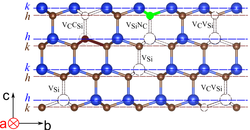
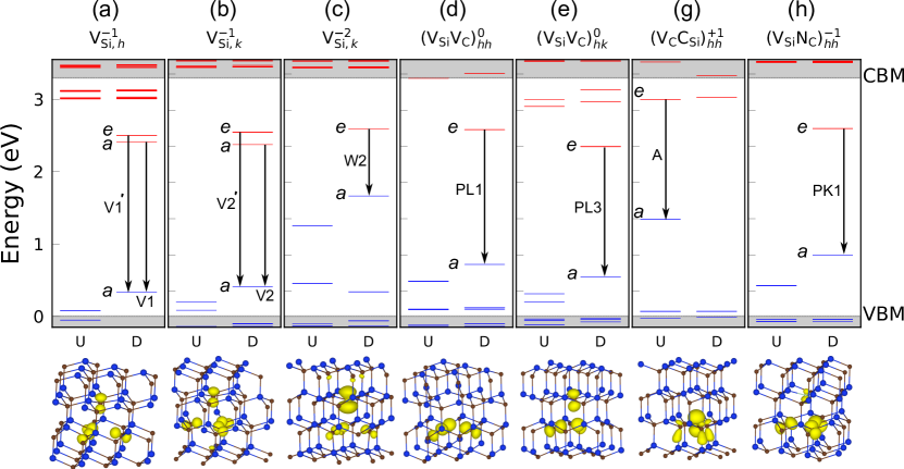
The defects considered in this work are illustrated in Fig. 1. For Si vacancies, we include the singly negative charge state (V) positioned at both h and k sites and doubly negative charge state (V) at k site Kobayashi et al. (2019); Gordon et al. (2015). Regarding divacancies (VV), we study configurations comprising a Si vacancy on an site in combination with C vacancies on either or sites. Finally, we include two variants of the NV-center in diamond, namely the positively charged VC and the negatively charged NV complexes. In total, there are thus seven centers and nine optical (charge neutral) transitions possible (Fig. 2).
Phonon calculations for large defect systems are computationally demanding. To accelerate these calculations we used regression as implemented in the hiphive package Eriksson et al. (2019). For each transition, training data was prepared by calculating the forces for the ground state structure using up to 125 configurations with random displacements, which were drawn from a normal distribution with a standard deviation of 0.01 Å. The interatomic force constants (IFCs) were then reconstructed using a cluster basis set with second-order cutoffs of 4.2 to 5.0 Å and optimized by least-squares regression. For all cases, the root-mean-square error over a holdout set that comprised 5% of the total available data was 17 meV/Å or lower. Finally, the IFCs were used to compute phonon frequencies and eigenvectors with the phonopy package Togo and Tanaka (2015).
III Results
III.1 Electronic structures and excitations
The 4H-SiC structure has hexagonal symmetry with the lattice constants and . Our results obtained using the PBEsol functional for the lattice constants are 3.08 Å and 10.08 Å. The electronic band gap from HSE06 calculations is found to be . These values are in good agreement with experimental data of , , and Lebedev (1999).
The defects considered here exhibit at least one occupied and one unoccupied defect state in the band gap, comprising a two-level optical system that involves states localized in the proximity of the defect. In Fig. 2 the electronic transitions are shown. Transitions are labeled in accordance with previous experimental studies except for V, for which no established label exists. All transitions were obtained by promoting an electron in the spin minority channels except for configuration A, for which the optical transition occurs in the majority spin channel. The ground state electronic configurations exhibit spin states , 1, 1, , and 1 for V, V, VV0, VC+1, and VN-1 centers, respectively. These values were experimentally and theoretically confirmed Janzén et al. (2009); Szász et al. (2015); Gali et al. (2010); Kuate Defo et al. (2018); Wang et al. (2020).
In the electronic ground state of V (Fig. 2a-b), four C dangling bonds point to the vacant site with their localized orbitals. V on an site is associated with transitions V1 and V1’, which correspond to HOMOLUMO and HOMOLUMO+1 transitions, respectively. Analogously, V on an site supports transitions V2 and V2’. The two transitions are separated by 116 meV and 172 meV, respectively, at and sites. The LUMO+1 states are doubly degenerate. Here the excited state is constructed by equally occupying each degenerate orbital.
Upon addition of one extra electron to V to obtain V, the electrons are still localized next to the vacant site (Fig. 2(c)). The charge distribution is mostly localized on the C atom placed at the same crystallographic site as vacant Si. In contrast to V, V can only host a single optical transition, labelled W2 for site. Previous formation energy calculations showed that the doubly negative Si vacancy is stable in charge state Kuate Defo et al. (2018), but the predicted PL line has not yet been experimentally observed. The W2 transition exhibit a ZPL energy of 0.72 eV, which is in the telecom wavelength (1 eV).
The neutral divacancies (Fig. 2d-e) can exhibit different symmetries depending on the local symmetry of the vacancy C and Si atoms. In order to restrict ourselves, we consider the HOMOLUMO transitions on the divacancy in and . Based on the KS spectra, additional transitions are possible in both and symmetry. The HOMOLUMO transition on is labelled PL1 and the HOMOLUMO transition on is labelled PL3. The electronic charge is equally distributed among the C atoms nearest to the silicon vacancy. It is noteworthy that the three nearest Si and C neighbors to the C and Si vacancy, respectively, relax inward toward the respective vacant site by 0.02 Å.
The singly charged carbon vacancy-carbon antisite defect VC+1 supports one transition labelled A, which occurs between two localized levels in the majority spin channel (Fig. 2g). Charge is mostly localized on the antisite carbon and to a lesser degree on its three nearest C neighbors. With 1.55 Å the C–C bond length is about 0.34 Å shorter than Si–C bonds in the ideal lattice.
Finally, the negatively charged silicon vacancy adjacent to a nitrogen that substitutes carbon, VN-1, which contains one additional electron compared to V, allows for a single optical transition based on the KS spectrum (Fig. 2h), which is labelled PK1. Only a very small part of the density of the unpaired electrons is found at the N atom. The defect resembles the axial VV divacancy with the Si–N bond length being about 0.11 Å shorter than Si–C bonds in ideal lattice.
Our calculated ZPL energies differ by less than 0.2 eV from the experimentally measured ones with the exception of the PK1 transition on VN-1 (Table 1), a level of accuracy that matches earlier calculations Davidsson et al. (2018). Generally, the good agreement with experiment of the calculated ZPL energies, as well as some of the other defect properties to be considered in the following, validates the defect assignments given in the literature.
| ZPL (eV) | (Å2 amu) | HRF | DWF (%) | ||||
|---|---|---|---|---|---|---|---|
| HSE06 | Expt. | PBEsol | PBEsol | PBEsol | Expt. | ||
| V | V1 | 1.57 | 1.44Shang et al. (2020) | 0.62 | 2.78 | 6.17 | 6–8Shang et al. (2020) |
| V1’ | 1.60 | 1.44Sörman et al. (2000) | 0.66 | 2.77 | 6.23 | — | |
| V2 | 1.24 | 1.35Shang et al. (2020) | 0.64 | 2.82 | 5.94 | 9.0Udvarhelyi et al. (2020) | |
| V2’ | 1.28 | — | 0.47 | 1.94 | 14.34 | — | |
| V | W2 | 0.72 | — | 0.30 | 1.47 | 22.97 | — |
| VV | PL1 | 1.14 | 1.10Koehl et al. (2011) | 0.71 | 2.75 | 6.39 | 5.3Christle et al. (2015) |
| PL3 | 1.25 | 1.12Falk et al. (2013) | 0.99 | 3.08 | 4.57 | 5.0Crook et al. (2020) | |
| VC | A | 1.69 | 1.88Castelletto et al. (2013) | 0.73 | 3.77 | 2.29 | — |
| NV | PK1 | 1.28 | 1.00von Bardeleben et al. (2015) | 0.70 | 2.64 | 7.09 | — |
III.2 Luminescence lineshapes
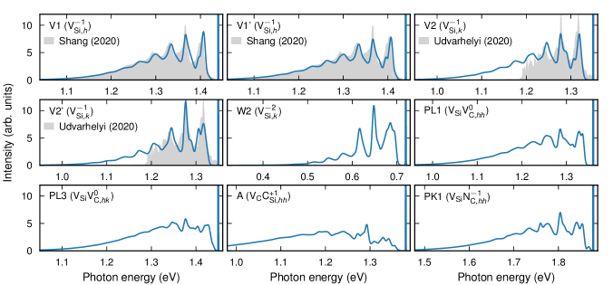
The calculated emission lineshapes are shown in Fig. 3, where the ZPLs have been shifted to the respective experimental value to simplify the comparison where applicable. The emission spectra consist of a sharp ZPL followed by a structured PSB at lower energy. It is evident from the results for the individual defects that the PSBs share some features: (i) the ZPLs are separated from the PSBs by an energy gap of about 30 meV, (ii) the broadening of the PSBs ranges from 200 to 500 meV, corresponding to the respective HRFs (Table 1), and (iii) smaller HRFs (number of created phonons) are associated with more structured PSBs.
The strength of the electron-phonon coupling can be partly assessed by the value (Table 1), which measures the magnitude of the geometric difference between initial and final state. It varies from 0.4 to 1.0 Å2amu for the W2 (V) and PL3 (VV) transitions showing the smallest and largest displacements, respectively. The DWFs varies from 2% to 23% with larger values implying a larger fraction of emission intensity in the ZPL. By this measure the V center, which has not been experimentally observed though, should be the best single photon emitter (SPE) candidate. The V2’ (V) transition results in a smaller lattice distortion at a value of 0.47 Å2amu compared with Å2amu (Table 1) for the other transitions on V. The PL1 (VV), PL3 (VV), and PK (NV) transitions exhibit the same but differ in HRFs (PK1 = PL1 PL3). As a result, one observes rather similar lineshapes, especially between PL1 and PK1, except for a hump at about 10 meV below the ZPL in the PK1 transition, which is due to a localized phonon. Although the inclusion of an adjacent V to the V in the transitions PL1 and PL3 modifies the position of the ZPL, it does not induce a dramatic change in the emission lineshape. The optical emission lineshape of the transition A (VC) with a tail of about 500 meV shows the widest PSB. We assign it to the contributions of high energy phonons and stronger coupling between electron and phonons during emission.
Our calculations for the V1/V1’ and V2/V2’ transitions involving V defects are in excellent agreement with experimental data Shang et al. (2020); Udvarhelyi et al. (2020). They yield similar lineshapes and the PSB width is about 300 meV.
The lineshape of the A transition has been measured Castelletto et al. (2013) at 120 K and was hypothesized to originate from the VC defect. The computed lineshape does not agree favorably with that measurement, which poses the question whether the measured transition is actually taking place on VC. The comparison with experimental data can also be made by using the DWF () values in Table 1 to benchmark our calculations. Only the experimentally reported DWF for the A transition (1%) Castelletto et al. (2013) deviates from our calculation (2.29%), which we attribute to the finite temperature effect present in the experiments. Overall, the calculations are in excellent agreement with experiments.
III.3 Vibrational modes analysis
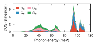
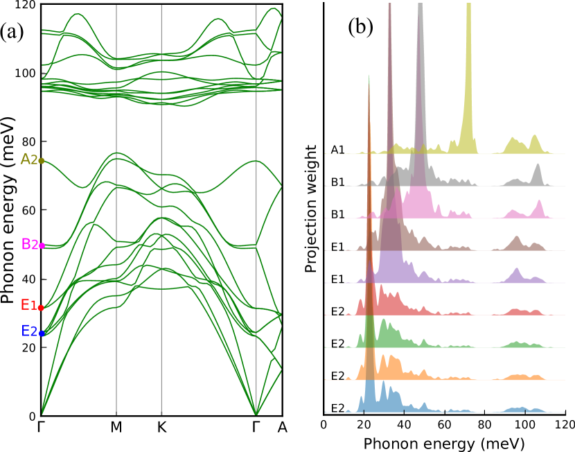
Our phonon calculations for the pristine system using a primitive unit cell (PUC) give the high energy Raman-active mode at 96.63 meV, which is in excellent agreement with the experimental value of 96.59 meV Wan et al. (2018). The phonon density of states (DOS) can be divided into two parts (Fig. 4). In the energy range up to 75 meV, the Si modes are dominant due to the larger mass of the Si atoms, while the double-peaked C-based modes are active at higher energies and centered at around 100 meV. The phonon band gap is about 14.2 meV starting from 76.4 meV. Note that we see a slight difference between the partial DOSs of atoms placed at and sites due to the different arrangement of second nearest neighbors.
To gain insight into the contribution of different vibrational modes to the PSBs, we now consider the electron-phonon coupling spectral functions (Eq. 3). To evaluate the localization of the modes in more details, we analyzed the IPR for the mode as Bell et al. (1970); Alkauskas et al. (2014)
| (5) |
IPR 1 if only one atom vibrates, while IPR if all atoms in the supercell vibrate with the same amplitude. Moreover, the localized vibrational modes that give rise to strong HRFs are collected and schematically illustrated.
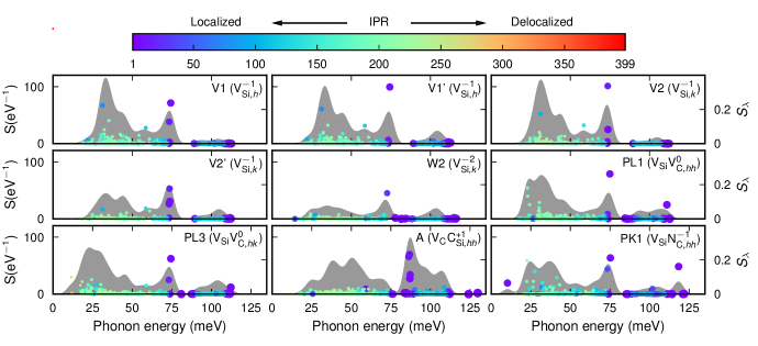
The electron-phonon spectral functions are shown in Fig. 5, accompanied by the plots of partial HRFs and IPR. The spectral function for the transitions on V (V1, V1’, and V2) show only minor differences while the V2’ transition can be clearly distinguished from the other three transitions. This is reflected in the HRF, which is about 2.8 for V1, V1’, and V2 while it is 1.9 for V2’.
Overall, the vibrational contribution to the transitions can be divided into (i) acoustic and optical bulk modes with energy less than 45 meV, e.g., the V1, V1’, and V2 transitions, and to a lesser extent the V2’ transition, which exhibits a pronounced peak at 35 meV. This peak is composed of several modes with IPR 100 (the maximal value of the IPR for this cell is 399). In other words, the peak is dominated by a single mode that has components of the bulk phonon displacement vector parallel to the carbon atoms adjacent to the vacancy site. (ii) Defect modes that are mostly located around the lower edge of the phonon band gap. In the V2 transition, the 73 meV peak can be attributed to two modes with relatively low IPR values of 8 and 18. In V2’, there are 3 modes (IPR between 9 and 18) that have HRFs between 0.09 and 0.18 making the total coupling in the region around 73 meV similar in strength to the other transitions. We note that there are many well localized modes (IPR ) at the high frequency edge 110 meV in all transitions on V. These modes do not however couple strongly to the transition displacement since the phonon displacement vectors are nearly perpendicular to the transition displacement. The W2 transition (V) resembles the V2’ spectral function with a weaker coupling to the vibrational degrees of freedom as indicated by the small total HRF of 1.47.
The coupling to the vibrational modes is similar between the transitions on divacancies (PL1 and PL3) as evident from the spectral functions and the similar HRFs of 2.75 and 3.08, respectively. The general features of the spectral functions are similar to the transitions on V, except the broader peaks at 20 to 50 meV. The strongest coupling is at 75 meV in both PL1 and PL3. The mode is a low IPR mode with values of 8 (7) in PL1 (PL3). In addition, the spectral weight in the high frequency range, around 100 meV, is slightly larger compared to the case of V. The peaks centered at 23 meV, 35 meV, and 48 meV originate predominantly from several delocalized (bulk) modes with IPR 100. The coupling to the vibrational modes is, however, much larger for the A transition than other considered transitions. The strongest coupling is to a set of four quasi-degenerate modes at the upper edge of the phonon band gap ( meV) with partial HRFs between 0.09 and 0.23.
For PK1 (NV), the coupling to the vibrational modes consists of three distinct bands at around meV, 75 meV and 120 meV. The localized vibrational mode around 10.3 meV is absent in other intrinsic centers. Its IPR value is 9. The peak centered at 75 meV results mainly from the coupling of two modes at 73 and 75 meV with HRFs of 41 and 8, respectively.
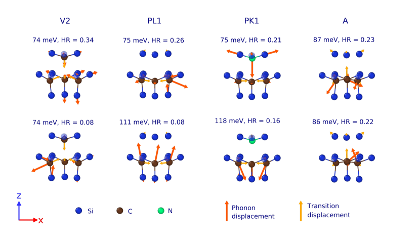
The selective vibrational modes and atomic displacements due to electron excitation are shown in Fig. 6. The dominant geometrical difference between the ground and excited states for all transitions on V is the radial motion (relative to the vacancy) of nearest neighbor carbon atoms, which displace by 0.08 Å in the case of V1 and 0.05 Å in the case of V1’. The displacements of atoms after relaxation for these defects are inward upon emission as shown for V2. These modes are quasi-degenerate and predominantly consists of motion of the nearest (relative to the vacancy) carbon atoms. The intensity of the 73 meV peak in the spectral function is, however, not weaker in the case of V2’ compared with the other transitions (V1, V1’, V2), although the displacement of nearest neighbor carbon atom is smaller. The phonon displacement for the 75 meV localized mode is shown for the case of PL1. During the transition, the closest C atoms to the silicon vacancy undergo the largest displacements towards the vacancy, while the Si atoms next to the C vacancy slightly move. In addition, the atomic vibrations mainly happen in the Si vacancy plane. At around 111 meV, there is a relatively weak, albeit stronger than in the case of V, coupling to modes with IPRs of around 5. The C atom displacements induced by transitions are almost perpendicular to vibrational motion. The local modes in the A transition are distributed over relatively few atoms. The CSi atom displaces the most during the transition towards the vacant carbon atom upon emission. Carbon atoms around and at the antisite are engaged in the atomic motions. In the PK1 transition at 75 meV the vibrational mode displaces the nearest Si atoms toward N. The mode at 118 meV, with an IPR of 7, originates from the strong vibrations of C atoms positioned in the same SiC plane as the vacancy. The structure relaxes around the vacant site.
To elucidate the symmetry of the participating phonons, we can decompose the modes that predominantly contribute to the spectral function of PL1 (Fig. 7). To this end, we project the supercell (SC) modes, , onto each of the PUC eigenmodes , at the -point
| (6) |
This analysis allows us to identify the respective bulk phonons by inspecting the similarity between atomic vibrations contributing to the PSB and unfolded -modes. 4H-SiC has point symmetry group where A1, B1, E1, and E2 are the vibrational modes at the -point Feldman et al. (1968). Both A1 and E1 modes are Raman- and IR-active, E2 is only Raman-active, while B1 is optically forbidden. We assign the 23 meV centered peak to the planar optical E2 modes. The doublets have a splitting of around 1 meV. The peak at 35 meV can originate from a mixed symmetry of planar acoustic (at M) and optical modes with symmetry of E1 Shang et al. (2020). The combination of axial optical and acoustic modes shape the spectral function peak at 48 meV. Indeed, we expect similar behaviour for other color centers.
IV Conclusions
In this work we have investigated the vibrational and associated optical properties of V, V, VV, VC, and NV defects in 4H-SiC. We compared the vibronic structure of different color centers by evaluating several important characteristics such as ZPLs, HRFs, DWFs as well as the structure of the PSBs. Our calculated DWFs and PSBs are in excellent agreement with the available experimental data. We found that the effect of charge state can be great on ZPL and DWF of V as it modifies the emission lineshape, whereas the lineshape does not differ between hh and hk pairs in VV. We identified few narrow peaks that correspond to multiphonon interactions. The PSB is feature-rich for smaller HRF values but shows a belly in the A transition due to strong electron-phonon coupling. Further, we predicted few localized vibrational modes around the phonon band gap that notably contribute to the PL spectra. Indeed, the electron transfer process to the ground state creates bulk acoustic phonons, though it is less-pronounced for VC color center. Overall our work thereby provides a reference database for single photon sources and spin qubits in 4H-SiC.
V Acknowledgements
This work has been supported by the Academy of Finland under Project No.311058 and the Knut and Alice Wallenberg Foundation (2014.0226). T. A.-N. has been supported in part by the academy of Finland QTF CoE grant No. 312298. We also thank CSC-IT Center Science Ltd. (Finland) and the Swedish National Infrastructure for Computing at PDC (Stockholm, Sweden) for generous grants of computer time. The authors also would like to thank professor Martti Puska for his support.
References
- Fisher and Barnes (1990) G. R. Fisher and P. Barnes, Philosophical Magazine B 61, 217 (1990).
- Weber et al. (2010) J. R. Weber, W. F. Koehl, J. B. Varley, A. Janotti, B. B. Buckley, C. G. Van de Walle, and D. D. Awschalom, Proceedings of the National Academy of Sciences 107, 8513 (2010), https://www.pnas.org/content/107/19/8513.full.pdf .
- Mélinon et al. (2007) P. Mélinon, B. Masenelli, F. Tournus, and A. Perez, Nature Materials 6, 479 (2007).
- Castelletto and Boretti (2020) S. Castelletto and A. Boretti, Journal of Physics: Photonics 2, 022001 (2020).
- Lohrmann et al. (2017) A. Lohrmann, B. C. Johnson, J. C. McCallum, and S. Castelletto, Reports on Progress in Physics 80, 034502 (2017).
- Aharonovich et al. (2016) I. Aharonovich, D. Englund, and M. Toth, Nature Photonics 10, 631 (2016).
- Lukin et al. (2020) D. M. Lukin, C. Dory, M. A. Guidry, K. Y. Yang, S. D. Mishra, R. Trivedi, M. Radulaski, S. Sun, D. Vercruysse, G. H. Ahn, and J. Vučković, Nature Photonics 14, 330 (2020).
- Awschalom et al. (2018) D. D. Awschalom, R. Hanson, J. Wrachtrup, and B. B. Zhou, Nature Photonics 12, 516 (2018).
- Son et al. (2020) N. T. Son, C. P. Anderson, A. Bourassa, K. C. Miao, C. Babin, M. Widmann, M. Niethammer, J. Ul Hassan, N. Morioka, I. G. Ivanov, F. Kaiser, J. Wrachtrup, and D. D. Awschalom, Applied Physics Letters 116, 190501 (2020).
- Eisaman et al. (2011) M. D. Eisaman, J. Fan, A. Migdall, and S. V. Polyakov, Review of Scientific Instruments 82, 071101 (2011).
- O’Brien et al. (2009) J. L. O’Brien, A. Furusawa, and J. Vučković, Nature Photonics 3, 689 (2009).
- Lodahl et al. (2015) P. Lodahl, S. Mahmoodian, and S. Stobbe, Rev. Mod. Phys. 87, 347 (2015).
- Gao et al. (2015) W. B. Gao, A. Imamoglu, H. Bernien, and R. Hanson, Nature Photonics 9, 363 (2015).
- Atatüre et al. (2018) M. Atatüre, D. Englund, N. Vamivakas, S.-Y. Lee, and J. a. Wrachtrup, Nature Reviews Materials 3, 38 (2018).
- Hensen et al. (215) B. Hensen, H. Bernien, A. E. Dréau, A. Reiserer, N. Kalb, M. S. Blok, J. Ruitenberg, R. F. L. Vermeulen, R. N. Schouten, C. Abellán, W. Amaya, V. Pruneri, M. W. Mitchell, M. Markham, D. J. Twitchen, D. Elkouss, S. Wehner, T. H. Taminiau, and R. Hanson, Nature 526, 682 (215).
- Bogdanov et al. (2017) S. Bogdanov, M. Y. Shalaginov, A. Boltasseva, and V. M. Shalaev, Opt. Mater. Express 7, 111 (2017).
- Boretti (2014) A. Boretti, Nature Photonics 8, 88 (2014).
- Lei et al. (2017) C. Lei, S. Peng, C. Ju, M.-H. Yung, and J. Du, Scientific Reports 7, 11937 (2017).
- Christle et al. (2017) D. J. Christle, P. V. Klimov, C. F. de las Casas, K. Szász, V. Ivády, V. Jokubavicius, J. Ul Hassan, M. Syväjärvi, W. F. Koehl, T. Ohshima, N. T. Son, E. Janzén, A. Gali, and D. D. Awschalom, Phys. Rev. X 7, 021046 (2017).
- Peng et al. (2009) T. H. Peng, Y. F. Lou, S. F. Jin, W. Y. Wang, W. J. Wang, G. Wang, and X. L. Chen, Powder Diffraction 24, 311–314 (2009).
- Wu and Guo (2008) I. J. Wu and G. Y. Guo, Phys. Rev. B 78, 035447 (2008).
- Kuate Defo et al. (2018) R. Kuate Defo, X. Zhang, D. Bracher, G. Kim, E. Hu, and E. Kaxiras, Phys. Rev. B 98, 104103 (2018).
- Gordon et al. (2015) L. Gordon, A. Janotti, and C. G. Van de Walle, Phys. Rev. B 92, 045208 (2015).
- Shang et al. (2020) Z. Shang, A. Hashemi, Y. Berencén, H.-P. Komsa, P. Erhart, S. Zhou, M. Helm, A. V. Krasheninnikov, and G. V. Astakhov, Phys. Rev. B 101, 144109 (2020).
- Udvarhelyi et al. (2020) P. Udvarhelyi, G. m. H. Thiering, N. Morioka, C. Babin, F. Kaiser, D. Lukin, T. Ohshima, J. Ul-Hassan, N. T. Son, J. Vučković, J. Wrachtrup, and A. Gali, Phys. Rev. Applied 13, 054017 (2020).
- Widmann et al. (2014) M. Widmann, S.-Y. Lee, T. Rendler, N. T. Son, H. Fedder, S. Paik, L.-P. Yang, N. Zhao, S. Yang, I. Booker, A. Denisenko, M. Jamali, S. A. Momenzadeh, I. Gerhardt, T. Ohshima, A. Gali, E. Janzén, and J. Wrachtrup, Nature Materials 14, 164 (2014).
- Sörman et al. (2000) E. Sörman, N. T. Son, W. M. Chen, O. Kordina, C. Hallin, and E. Janzén, Phys. Rev. B 61, 2613 (2000).
- Davidsson et al. (2018) J. Davidsson, V. Ivády, R. Armiento, N. T. Son, A. Gali, and I. A. Abrikosov, New Journal of Physics 20, 023035 (2018).
- Koehl et al. (2011) W. F. Koehl, B. B. Buckley, F. J. Heremans, G. Calusine, and D. D. Awschalom, Nature 479 (2011), 10.1038/nature10562.
- Falk et al. (2014) A. L. Falk, P. V. Klimov, B. B. Buckley, V. Ivády, I. A. Abrikosov, G. Calusine, W. F. Koehl, A. Gali, and D. D. Awschalom, Phys. Rev. Lett. 112, 187601 (2014).
- Wolfowicz et al. (2017) G. Wolfowicz, C. P. Anderson, A. L. Yeats, S. J. Whiteley, J. Niklas, O. G. Poluektov, F. J. Heremans, and D. D. Awschalom, Nature Communications 8, 1876 (2017).
- Christle et al. (2015) D. J. Christle, A. L. Falk, P. Andrich, P. V. Klimov, J. U. Hassan, N. T. Son, E. Janzén, T. Ohshima, and D. D. Awschalom, Nature Materials 14, 160 (2015).
- Umeda et al. (2006) T. Umeda, N. T. Son, J. Isoya, E. Janzén, T. Ohshima, N. Morishita, H. Itoh, A. Gali, and M. Bockstedte, Phys. Rev. Lett. 96, 145501 (2006).
- Umeda et al. (2007) T. Umeda, J. Ishoya, T. Ohshima, N. Morishita, H. Itoh, and A. Gali, Phys. Rev. B 75, 245202 (2007).
- Szász et al. (2015) K. Szász, V. Ivády, I. A. Abrikosov, E. Janzén, M. Bockstedte, and A. Gali, Phys. Rev. B 91, 121201 (2015).
- Castelletto et al. (2013) S. Castelletto, B. C. Johnson, V. Ivády, N. Stavrias, A. Umeda, T. Gali, and T. Ohshima, Nature Materials 13, 151 (2013).
- Steeds (2009) J. W. Steeds, Phys. Rev. B 80, 245202 (2009).
- Csóré et al. (2017) A. Csóré, H. J. von Bardeleben, J. L. Cantin, and A. Gali, Phys. Rev. B 96, 085204 (2017).
- Hong et al. (2013) S. Hong, M. S. Grinolds, L. M. Pham, D. Le Sage, L. Luan, R. L. Walsworth, and A. Yacoby, MRS Bulletin 38, 155–161 (2013).
- Wang et al. (2020) J.-F. Wang, J.-M. Cui, F.-F. Yan, Q. Li, Z.-D. Cheng, Z.-H. Liu, Z.-H. Lin, J.-S. Xu, C.-F. Li, and G.-C. Guo, Phys. Rev. B 101, 064102 (2020).
- von Bardeleben et al. (2015) H. J. von Bardeleben, J. L. Cantin, E. Rauls, and U. Gerstmann, Phys. Rev. B 92, 064104 (2015).
- Zargaleh et al. (2018a) S. A. Zargaleh, S. Hameau, B. Eble, F. Margaillan, H. J. von Bardeleben, J. L. Cantin, and W. Gao, Phys. Rev. B 98, 165203 (2018a).
- Zargaleh et al. (2018b) S. A. Zargaleh, H. J. von Bardeleben, J. L. Cantin, U. Gerstmann, S. Hameau, B. Eblé, and W. Gao, Phys. Rev. B 98, 214113 (2018b).
- Walker (1979) J. Walker, Reports on Progress in Physics 42, 1605 (1979).
- Bradac et al. (2019) C. Bradac, W. Gao, J. Forneris, M. E. Trusheim, and I. Aharonovich, Nature Communications 10, 5625 (2019).
- Maze et al. (2008) J. R. Maze, P. L. Stanwix, J. S. Hodges, S. Hong, J. M. Taylor, P. Cappellaro, L. Jiang, M. V. G. Dutt, E. Togan, A. S. Zibrov, A. Yacoby, R. L. Walsworth, and M. D. Lukin, Nature 455, 644 (2008).
- Johnson et al. (2015) S. Johnson, P. R. Dolan, T. Grange, A. A. P. Trichet, G. Hornecker, Y. C. Chen, L. Weng, G. M. Hughes, A. A. R. Watt, A. Auffèves, and J. M. Smith, New Journal of Physics 17, 122003 (2015).
- Yan et al. (2020) X. Yan, P. Li, L. Kang, S.-H. Wei, and B. Huang, Journal of Applied Physics 127, 085702 (2020).
- Kobayashi et al. (2019) T. Kobayashi, K. Harada, Y. Kumagai, F. Oba, and Y.-i. Matsushita, Journal of Applied Physics 125, 125701 (2019).
- Torpo et al. (2002) L. Torpo, T. E. M. Staab, and R. M. Nieminen, Phys. Rev. B 65, 085202 (2002).
- Lax (1952) M. Lax, The Journal of Chemical Physics 20, 1752 (1952).
- Miyakawa and Dexter (1970) T. Miyakawa and D. L. Dexter, Phys. Rev. B 1, 2961 (1970).
- Alkauskas et al. (2014) A. Alkauskas, B. B. Buckley, D. D. Awschalom, and C. G. V. de Walle, New Journal of Physics 16, 073026 (2014).
- Blöchl (1994) P. E. Blöchl, Physical Review B 50, 17953 (1994).
- Kresse and Joubert (1999) G. Kresse and D. Joubert, Physical Review B 59, 1758 (1999).
- Kresse and Furthmüller (1996) G. Kresse and J. Furthmüller, Computational Materials Science 6, 15 (1996).
- Kresse and Hafner (1993) G. Kresse and J. Hafner, Physical Review B 47, 558 (1993).
- Perdew et al. (2008) J. P. Perdew, A. Ruzsinszky, G. I. Csonka, O. A. Vydrov, G. E. Scuseria, L. A. Constantin, X. Zhou, and K. Burke, Phys. Rev. Lett. 100, 136406 (2008).
- Krukau et al. (2006) A. V. Krukau, O. A. Vydrov, A. F. Izmaylov, and G. E. Scuseria, The Journal of Chemical Physics 125, 224106 (2006).
- Eriksson et al. (2019) F. Eriksson, E. Fransson, and P. Erhart, Advanced Theory and Simulations 2, 1800184 (2019).
- Togo and Tanaka (2015) A. Togo and I. Tanaka, Scr. Mater. 108, 1 (2015).
- Lebedev (1999) A. A. Lebedev, Semiconductors 33, 107 (1999).
- Janzén et al. (2009) E. Janzén, A. Gali, P. Carlsson, A. Gällström, B. Magnusson, and N. T. Son, Physica B: Condensed Matter 404, 4354 (2009).
- Gali et al. (2010) A. Gali, A. Gällström, N. T. Son, and E. Janzén, in Silicon Carbide and Related Materials 2009, Materials Science Forum, Vol. 645 (Trans Tech Publications Ltd, 2010) pp. 395–397.
- Falk et al. (2013) A. L. Falk, B. B. Buckley, G. Calusine, W. F. Koehl, V. V. Dobrovitski, A. Politi, C. A. Zorman, P. X.-L. Feng, and D. D. Awschalom, Nature Communications 4, 1819 (2013).
- Crook et al. (2020) A. L. Crook, C. P. Anderson, K. C. Miao, A. Bourassa, H. Lee, S. L. Bayliss, D. O. Bracher, X. Zhang, H. Abe, T. Ohshima, E. L. Hu, and D. D. Awschalom, Nano Letters 20, 3427 (2020), pMID: 32208710.
- Stukowski (2010) A. Stukowski, Modelling and Simulation in Materials Science and Engineering 18, 015012 (2010).
- Wan et al. (2018) L. Wan, D. Zhao, F. Wang, G. Xu, T. Lin, C.-C. Tin, Z. Feng, and Z. C. Feng, Opt. Mater. Express 8, 119 (2018).
- Bell et al. (1970) R. J. Bell, P. Dean, and D. C. Hibbins-Butler, Journal of Physics C: Solid State Physics 3, 2111 (1970).
- Feldman et al. (1968) D. W. Feldman, J. H. Parker, W. J. Choyke, and L. Patrick, Phys. Rev. 173, 787 (1968).