Optical-microwave pump-probe studies of electronic properties in novel materials
Abstract
Combined microwave-optical pump-probe methods are emerging to study the quantum state of spin qubit centers and the charge dynamics in semiconductors. A major hindrance is the limited bandwidth of microwave irradiation/detection circuitry which could be overcome with the use of broadband coplanar waveguides (CPW). We present the development and performance characterization of two spectrometers: an optically detected magnetic resonance spectrometer (ODMR) and a microwave detected photoconductivity measurement. In the first method light serves as detection and microwaves excite the investigated medium, while in the second the roles are interchanged. The performance is demonstrated by measuring ODMR maps on the nitrogen-vacancy center in diamond and time resolved photoconductivity in p-doped silicon. The results demonstrate both an efficient coupling of the microwave irradiation to the samples as well as an excellent sensitivity for minute changes in sample conductivity.
I Introduction
Optical pump-probe spectroscopy and microscopy experiments represent an important branch of tools to study the conduction dynamics in novel materials Fischer et al. (2016) or non-equilibrium states Lee et al. (2020). Alternatively, electromagnetic radiation with very different wavelength can be combined in a similar pump-probe way, which enables to study physical phenomena occurring on the different energy scales. The combined microwave-optical pump probe methods enable for example to detect microwave induced spin transitions with optics, a method known as optically detected magnetic resonance (ODMR). The reverse situation occurs in microwave detected photoconductivity (-PCD), where optically induced non-equilibrium charge carriers cause a change in the reflected microwave intensity, thus enabling a study of charge recombination in a time resolved manner. ODMR Lund and Shiotani (2003) spectroscopy is a powerful tool to study the spin states of novel systems such as carbon nanotubes Stich et al. (2014), fullerenes Lane et al. (1992) and nitrogen-vacancy centers in diamond Gruber et al. (1997) for applications in spintronics Neumann et al. (2009), quantum computing Harneit et al. (2002) or light emitting diodes Shinar (2012). This technique benefits from the high energy resolution of the microwaves (down to a few 100 kHz, i.e. neV energy range) with the high efficiency of optical photon detection. It is even possible to detect the change in luminescence of a single molecule Wrachtrup et al. (1993). Microwave detected photoconductivity decay measurement (-PCD) Kunst and Beck (1986) is widely used in semiconductor industry to study impurity concentration in silicon wafers Berger et al. (2011) or non-silicon semiconductors such as CdTe Novikov et al. (2010). This contactless method enables manufacturers to determine impurity concentrations with great accuracy and researchers to gain information on charge carrier dynamics on the nanosecond timescale. A key element of the instruments in both cases is the microwave irradiation unit, which is most often a resonator, offering a high microwave power to electric or magnetic field conversion due to the resonator quality factor, at the cost of a reduced bandwidth. Alternatively, microwave antennas Sasaki et al. (2016) are often used but these have usually smaller bandwidth and worse microwave power to magnetic field conversion ratio. In principle compact, non-resonant waveguides combine both the large bandwidth with the good filling factor, which results in an excellent microwave power to magnetic field conversion. Coplanar waveguides Wen (1969); Jia et al. (2018) and slot lines Cohn (1969) consist of metallic lines placed on high dielectric constant substrates. This layout confines the microwave fields traveling in a quasi-TEM mode Simons (2002) to a small volume giving a huge electromagnetic energy density competing with classical resonators. These miniaturized waveguides can be combined with surface mount devices (SMDs) Gustrau (2012) and other circuit elements. CPWs also opened a way towards microwave device miniaturization such as production of millimeter-scale circulators Yamamoto et al. (2004). In case of resonators, the access to the sample such as optical illumination or application of external electric field is limited and it affects the performance of the resonator, e.g. a window on the wall of the resonator lowers the -factor. The broadband operation of CPWs makes frequency swept experiments such as permeability measurement Cho et al. (2007) and ferromagnetic resonance studies Yuan et al. (2014) also very effective. Herein, we present the development and performance characterization of two instruments, which both operate with coplanar waveguides. We present a broadband optically detected magnetic resonance spectrometer which allowed to study quantum states of nitrogen-vacancy centers in diamond. The microwave detected photoconductivity decay instrument has a good sensitivity for small changes in sample conductivity during the transient decay of the charge carriers.
II The spectrometer setups
II.1 The ODMR spectrometer
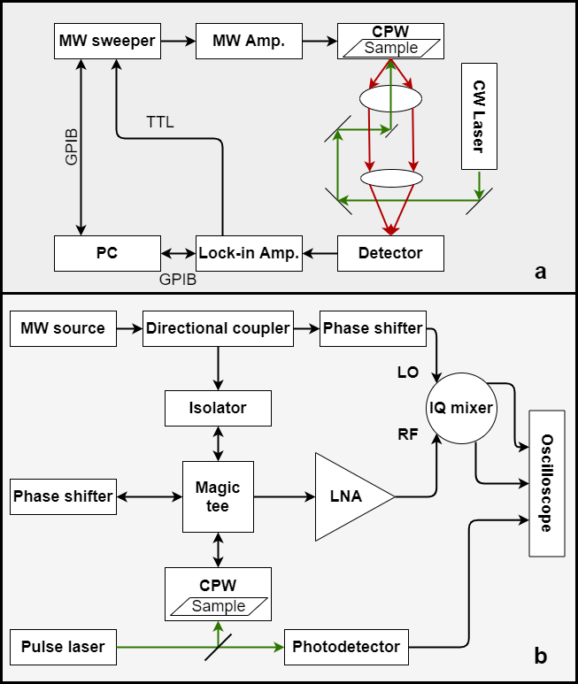
The setup of the optically detected magnetic resonance spectrometer is shown in Fig. 1. The coplanar waveguide holding the sample is illuminated using a continuous wave laser ( Coherent Verdi 5G frequency doubled Nd:YAG). The luminescent light is collected and focused by the so called ”image relay” consisting of an achromatic doublet pair (Thorlabs MAP1030100-B) to a spectrograph (Horiba JY iHR320) equipped with a photomultiplier tube (Hamamatsu R2658P) and a single pixel InGaAs detector (Horiba DSS-IGA010L). The former covers the ultraviolet (UV) to near infrared (NIR) range (), while the latter is optimized for the NIR range (). The detector output is connected to a lock-in amplifier (Stanford Research Systems, SR830) through a transimpedance amplifier. The output of the microwave signal generator (HP83751B) is chopped by the TTL signal coming from the lock-in amplifier. The microwaves are fed into an amplifier (Kuhne KuPa 270330-10A, ) and then sent to the CPW which has a termination at its end. The CPW is placed on a two-axis miniature dovetail translation stage (Thorlabs DT12XY/M) during room temperature measurements. To apply external magnetic field, the stage and the other optics parts are placed on a rail that can be rolled into the middle of an electromagnet with a magnetic field up to 1.2 T.
II.2 The microwave detected photoconductivity decay spectrometer
Fig. 1 shows the microwave photoconductivity decay measurement setup which is a modification of our previous resonator-based, time resolved -PCD setup described elsewhere Gyüre-Garami et al. (2019). A Q-switch pulsed laser ( Coherent Evolution-15, frequency doubled Nd:YLF) with repetition rate, pulse energy of and pulse width of is used for excitation of charge carriers in the sample placed on the CPW.
The microwave oscillator (Kuhne MKU LO 8-13 PLL) serves as the source of the probing MW field and as the local oscillator of a double-balanced IQ mixer. The directional coupler sends half of the incoming power through an isolator (to avoid damage of the oscillator unit by reflected power) to the magic tee, the other half drives the IQ mixer. Half of the incoming microwave power is directed towards the CPW, the other half to the port with a phaseshifter and a variable attenuator attached. The waves reflected from the CPW and the other port interfere with each other on the 4th port allowing us to get rid off the DC reflection by setting the attenuation and phase properly. The previously described MW bridge is followed by a low noise amplifier (JaniLab Inc. ) and the amplified signal is fed to the IQ mixer. The I (in-phase) and Q (quadrature) signals downconverted from the detected RF signal are digitized with an oscilloscope (Tektronix MDO-3024, ) which is triggered by the signal coming from the photodetector (Thorlabs DET36A/M) sensing the laser pulse.
II.3 The cryostat
To carry out cryogenic measurement we built a closed cylindrical compartment with optical access through a quartz window (1”) and MW connection using an UHV SMA connector. The CPW is fixed to a copper cube attached to the inner tube that can be filled with liquid nitrogen from the outside. The space between the two tubes where the CPW is placed is evacuated using a turbomolecular pump (Pfeiffer HiCube Eco). Vacuum level of is easily achievable and grants long enough measurement time without any condensation problems on the outside or heating of the sample.
II.4 Samples
ODMR measurements were performed on single crystal () Type-Ib diamond samples (Element Six Ltd.) produced by high pressure high temperature method (HPHT), containing less than substitutional nitrogen. After neutron irradiation of the diamond plates in the Training Reactor of the Institute of Nuclear Techniques (located at the Budapest University of Technology and Economics) for 8 hours at 100 kW power with total fluence of appx. ( in the - range), the samples were annealed under dynamic vacuum () at to help the diffusion of vacancies creating the nitrogen-vacancy centers. To dissolve surface contamination, samples were put into vials containing a mixture of acetone and isopropyl-alcohol and bath-sonicated for 15 minutes.
Microwave detected photoconductivity decay measurements were carried out on phosphorus doped silicon wafer with an approximate surface of and thickness of . The resistivity of the sample was cm, as determined by a four-point sheet resistivity measurement technique.
III Spectrometer characterization
III.1 ODMR on NV centers in diamond
Here, we present a range of measurements to demonstrate the versatile applicability of coplanar waveguides. First, ODMR measurements in variable external magnetic fields are shown along with a wavelength resolved zero field ODMR map. We carried out ODMR measurements on diamond samples to demonstrate the advantages of applying CPWs for MW irradiation. Fig. 2 shows microwave frequency sweeps performed in zero magnetic field and also in .
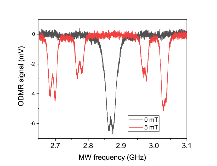
These spectra were acquired in a constant external magnetic field while the microwave frequency was swept and chopped by the TTL signal of the lock-in amplifier. Fig. 3 on the other hand shows a magnetic field sweep at constant microwave frequency of . Here the MW amplifier was replaced with one working in the X-band (Kuhne KuPa 9001250-2A, ). This detection method is essentially the same as if it was a conventional electron spin resonance but the signal is detected optically. The principle of detection is that the microwave field is frequency modulated using the lock-in amplifiers local oscillator as a sine source connected to the microwave oscillator. In Fig. 3. the intensity of such ODMR signal is examined as the amplitude of the modulating sine wave increases. The modulation depth was set to meaning a maximum deviation of in this measurement, however, above no significant increase in the ODMR amplitude can be seen.
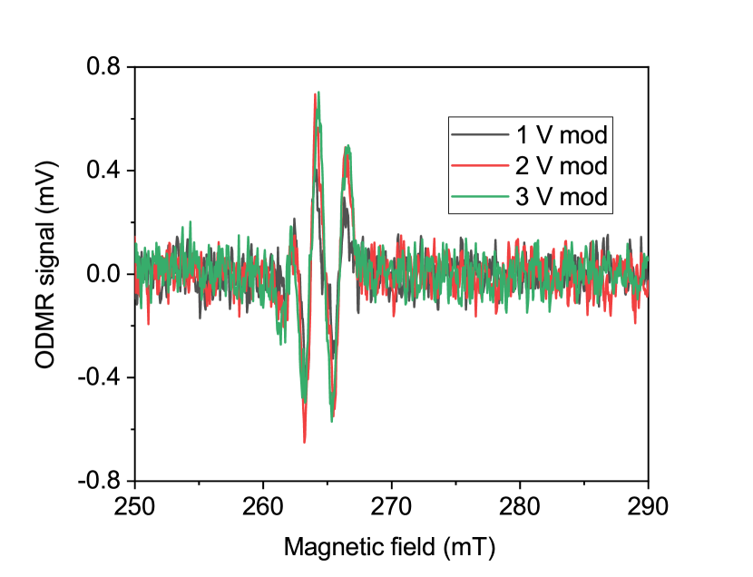
Fig. 4. shows individual ODMR spectra combined together to form a so-called ODMR map. This closely resembles emission-excitation maps used in photoluminescence, with the exception that one axis is the microwave frequency, while the other is the wavelength of the emitted light. This measurement was carried out in zero external magnetic field in the form of wavelength sweeps at fixed MW frequency. Here, the microwave sweeper is set to continuous-wave mode and wavelength resolved photoluminescence (PL) is recorded as the grating of the spectrometer is rotated. In our setup, we simultaneously detect the DC voltage (the PL signal) and the AC component (the signal detected by the lock-in amplifier) which is the ODMR signal.
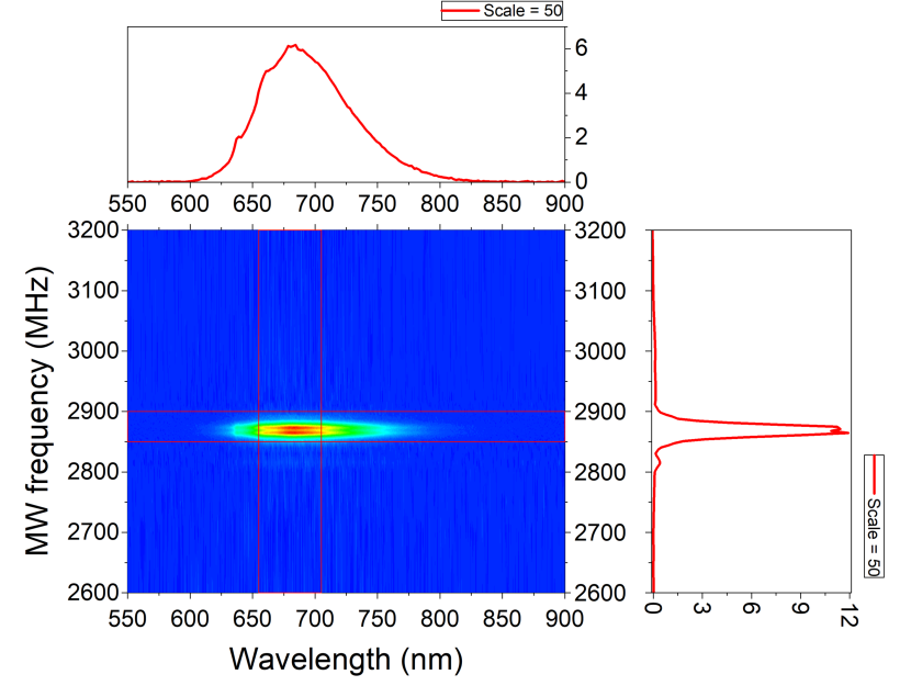
The measurement time is determined by the required resolution and range in wavelength and microwave frequency and the integration time. The map presented in Fig. 4 was recorded with wavelength resolution and integration time. The microwave frequency resolution is in the middle and was changed in bigger steps () moving away from the resonance resulting in different values. Altogether, this results in measurement time of minutes.
III.2 -PCD on silicon wafers
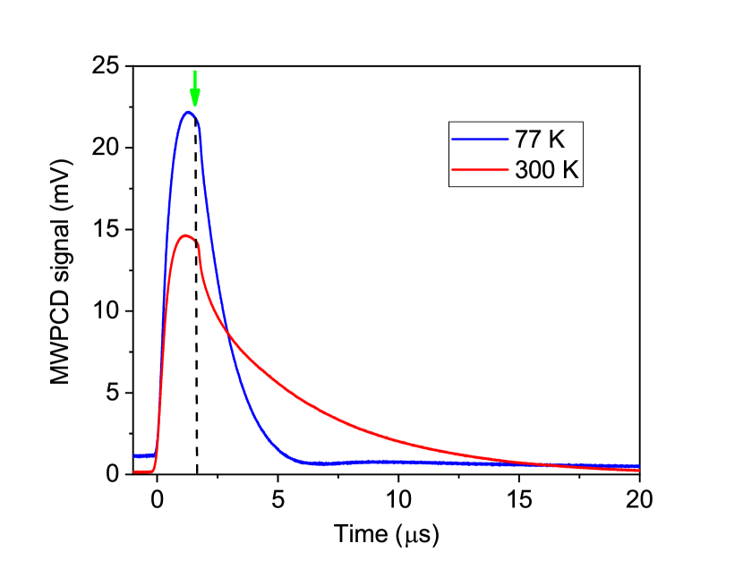
Fig. 5 shows the microwave detected photoconductivity decay (or the -PCD signal) measured on a phosphorus doped silicon sample at room temperature and at . The signal magnitude was obtained from the square root of the squared sum of the I and Q components. The coplanar waveguide can be readily adapted to cryostat experiments as it can be conveniently placed on the cold finger of an arbitrary cryostat. In contrast, a microwave resonator usually suffers from a change in the resonant frequency (and the quality factor) as a function of the temperature which affects the measurement sensitivity and also care is required to tune the source frequency to the of the resonator eigenfrequency. The CPW design is free from all these complications.
In case of time resolved microwave detection, the use of microwave resonators is also impractical as the resonator bandwidth (typically 100 kHz-1 MHz) significantly limits the available time resolution Gyüre-Garami et al. (2019). The typical power to microwave field conversion is for a TE011 type cylindrical cavity. Following the calculations presented in Ref. Simons and Arora (1982) for our CPW with gaps of separated by and total width of , this factor is . This means that the CPW performs as a cavity with a Q-factor of 4000.
As Fig. 5 demonstrates, the cooling leads to shortening of charge carrier lifetime in the investigated material. This is described by the Shockley-Read-Hall theory Hall (1952). The impurities introduce empty gap states thus giving a rise to recombination. However, these levels can be occupied by thermally excited electrons. With decreasing temperature, fewer states are occupied therefore more recombination centers are present in the sample and the optically excited electrons have a shorter lifetime.
IV Summary
We presented the development of an ODMR spectrometer and a microwave photoconductivity decay measurement setup. Both instrument benefit from the coplanar waveguide structure, namely the easy optical access to the sample compared to classical microwave resonators and the broadband operation. Low temperature -PCD measurements reveal decreasing carrier lifetime as the silicon sample is cooled. We pointed out that in specific cases resonators can outperform CPWs in terms of accuracy and sensitivity, but their advantage turns out to be a disadvantage when one needs to change measurement parameters such as microwave frequency or sample temperature. The fast -PCD setup could reveal information on charge carrier dynamics in intensively studied novel photovoltaic materials such as methylammonium halide perovskites.
V Acknowledgement
Work was supported by the Hungarian National Research, Development and Innovation Office (NKFIH) Grant Nr. K119442 and 2017-1.2.1-NKP-2017-00001.
References
- Fischer et al. (2016) M. C. Fischer, J. W. Wilson, F. E. Robles, and W. S. Warren, Rev. Sci. Instrum. 87, 031101 (2016).
- Lee et al. (2020) C. Lee, T. Rohwer, E. J. Sie, A. Zong, E. Baldini, J. Straquadine, P. Walmsley, D. Gardner, Y. S. Lee, I. R. Fisher, and N. Gedik, Rev. Sci. Instrum. 91, 043102 (2020).
- Lund and Shiotani (2003) A. Lund and M. Shiotani, eds., EPR of Free Radicals in Solids (Springer, 2003).
- Stich et al. (2014) D. Stich, F. Späth, K. Hannes, A. Sperlich, V. Dyakonov, and T. Hertel, Nat. Photonics 8, 139 (2014).
- Lane et al. (1992) P. A. Lane, L. S. Swanson, Q.-X. Ni, J. Shinar, J. P. Engel, T. J. Barton, and L. Jones, Phys. Rev. Lett. 68, 887 (1992).
- Gruber et al. (1997) A. Gruber, A. Dräbenstedt, C. Tietz, L. Fleury, J. Wrachtrup, and C. von Borczyskowski, Science 276, 2012 (1997).
- Neumann et al. (2009) P. Neumann, R. Kolesov, V. Jacques, J. Beck, J. Tisler, A. Batalov, L. Rogers, N. B. Manson, G. Balasubramanian, F. Jelezko, and J. Wrachtrup, New J. Phys. 11, 013017 (2009).
- Harneit et al. (2002) W. Harneit, C. Meyer, A. Weidinger, D. Suter, and J. Twamley, Phys. Status Solidi B 233, 453 (2002).
- Shinar (2012) J. Shinar, Laser Photonics Rev. 6, 767 (2012).
- Wrachtrup et al. (1993) J. Wrachtrup, C. von Borczyskowski, J. Bernard, M. Orrit, and R. Brown, Phys. Rev. Lett. 71, 3565 (1993).
- Kunst and Beck (1986) M. Kunst and G. Beck, J. Appl. Phys. 60, 3558 (1986).
- Berger et al. (2011) B. Berger, N. Schüler, S. Anger, B. Gründig-Wendrock, J. R. Niklas, and K. Dornich, Phys. Status Solidi A 208, 769 (2011).
- Novikov et al. (2010) G. F. Novikov, A. A. Marinin, and E. V. Rabenok, Instruments and Experimental Techniques 53, 83 (2010).
- Sasaki et al. (2016) K. Sasaki, Y. Monnai, S. Saijo, R. Fujita, H. Watanabe, J. Ishi-Hayase, K. M. Itoh, and E. Abe, Rev. Sci. Instrum. 87, 053904 (2016).
- Wen (1969) C. P. Wen, IEEE Trans. Microw. Theory Tech. 17, 1087 (1969).
- Jia et al. (2018) W. Jia, Z. Shi, X. Qin, X. Rong, and J. Du, Rev. Sci. Instrum. 89, 064705 (2018).
- Cohn (1969) S. B. Cohn, IEEE Trans. Microw. Theory Tech. 17, 768 (1969).
- Simons (2002) R. Simons, Coplanar Waveguide Circuits, Components, and Systems (Wiley, 2002).
- Gustrau (2012) F. Gustrau, RF and Microwave Engineering (Wiley, 2012).
- Yamamoto et al. (2004) S. Yamamoto, K. Shitamitsu, H. Kurisu, M. Matsuura, K. Oshiro, H. Mikami, and S. Fujii, Phys. Status Solidi B 241, 1769 (2004).
- Cho et al. (2007) S. G. Cho, J. Kim, I. Kim, K. H. Kim, and M. Yamaguchi, Phys. Status Solidi A 204, 4133 (2007).
- Yuan et al. (2014) L. Yuan, Z. Yue, S. Meng, and L. Li, Phys. Status Solidi A 211, 1828 (2014).
- Gyüre-Garami et al. (2019) B. Gyüre-Garami, B. Blum, O. Sági, A. Bojtor, S. Kollarics, G. Csősz, B. G. Márkus, J. Volk, and F. Simon, J. Appl. Phys. 126, 235702 (2019).
- Simons and Arora (1982) R. N. Simons and R. K. Arora, IEEE Trans. Microw. Theory Tech. 30, 1094 (1982).
- Hall (1952) R. N. Hall, Phys. Rev. 87, 387 (1952).