Controlled Exciton-Plasmon Coupling in a Mixture of Ultrathin Periodically Aligned SingleWall Carbon Nanotube Arrays
Abstract
We study theoretically the in-plane electromagnetic response and the exciton-plasmon interactions for an experimentally feasible carbon nanotube (CN) film systems composed of parallel aligned periodic semiconducting CN arrays embedded in an ultrathin finite-thickness dielectric. For homogeneous single-CN films, the intertube coupling and thermal broadening bring the exciton and interband plasmon resonances closer together. They can even overlap due to the inhomogeneous broadening for films composed of array mixtures with a slight CN diameter distribution. In such systems the real part of the response function is negative for a broad range of energies (negative refraction band), and the CN film behaves as a hyperbolic metamaterial. We also show that for a properly fabricated two-component CN film, by varying the relative weights of the two constituent CN array components one can tune the optical absorption profile to make the film transmit or absorb light in the neighborhood of an exciton absorption resonance on-demand.
I Introduction
Carbon Nanotubes (CNs) and ultrathin films made of periodic CN arrays, provide a variety of useful physical properties that are essential for optoelectronic device applications Bondarev2009 ; MaYa2011 ; VoEtAl2013 ; AaFrPe2008 ; WuEtAl2017 . Periodically aligned CN array films, in particular, provide stability and precise tunability of their characteristics by means of the CN diameter, intertube distance and film thickness variation, which is why they are getting more and more attention of experimental communities RoEtal2019 ; HERTEL2013 ; ZhEtal2020 ; FaEtAl2017 ; HoEtAl2018 ; KuCh2017 . Self-assembled quasi-periodic finite-thickness single-wall CN (SWCN) films have been recently shown experimentally to exhibit extraordinary optoplasmonic properties such as a tunable negative dielectric response in a broad range of the photon excitation energies RoEtal2019 . Using the Maxwell-Garnett (MG) mixing method Ma2016 and the many-particle Green’s function formalism Mahan2000 , we have lately explained this theoretically to be the case due to the inhomogeneous broadening effect in films composed of mixed SWCN arrays with a narrow nanotube diameter distribution AdBo_MA2020 .
In this contribution, we focus on the exciton-plasmon coupling in a two-component mixture of periodic SWCN arrays. We start with the analysis of the dielectric response of a homogeneous quasi-2D array of parallel aligned, uniformly spaced, identical SWCNs immersed in a finite-thickness dielectric medium of static relative dielectric permittivity , sandwiched between a substrate and a superstrate of relative permittivities and . A schematic of the array system under study and notations of relevance are presented in the inset of Fig. 1. Next, we present a numerical study on the role of the exciton-plasmon coupling in the optical absorption spectrum of a two-component mixture of the homogeneous SWCN arrays. We discuss how this coupling and thereby the absorption can be controlled by varying the relative weights of the individual components in the mixture.
The SWCNs are aligned along the -axis in a dielectric layer of thickness with the intertube center-to-center distance . The electron charge density is distributed uniformly all over the periodic cylindrical nanotube surfaces, whereby the pairwise electron Coulomb interaction in the system of CNs can be approximated by that of two uniformly charged rings of radius of the respective -th and -th tubules Bo2019ME . We consider that the dielectric medium embedding a periodic array has much greater dielectric permittivity than the substrate and superstrate permittivities. In this case Ke1980 , the Coulomb interaction in the film increases strongly as the film thickness decreases, making the Coulomb interaction independent of the vertical coordinate component Ke1980 ; BoSh2017 ; BoMoSh2018 ; Bo2019ME ; BoMoSh2020 . Although this vertical confinement leads to the reduction of the effective dimensionality from three to two, the thickness is still a variable parameter there to represent the finite vertical size of the system, which the dielectric response of the film depends on.
We proceed with our studies as follows. First, we determine the conductivity of an individual SWCN as a function of photon frequency using the so-called -band structure method Ando2005 . Then, taking advantage of the vertical electron confinement nature of stronger Keldysh-Rytova interaction potential Ke1980 ; BoSh2017 ; BoMoSh2018 ; Bo2019ME , we determine the effective interaction of an ultrathin finite-thickness periodically aligned CN array and derive an expression for the dynamical dielectric response tensor of the CN-array using the low-energy plasmonic response calculation technique Bo2019ME and the many-particle Green’s function formalism Mahan2000 . We then mix two non-identical CN arrays using the Maxwell-Garnett mixing scheme Ma2016 and examine what happens on a CN film’s absorption spectrum if the film has only a few non-identical homogeneous CN arrays with possible exciton-plasmon coupling presence.
Previously, the exciton-plasmon coupling was studied for a variety of nanostructured systems such as organic semiconductors, SiC nanocrystals, gold nanoshells and nanorods, metallic dimers, and hybrid metal-semiconductor nanostructures BeEtal2004 ; ScEtal2013 ; MaEtal2011 ; FeEtal2007 ; Dai_2012 ; VaEtal2008 ; WuEtal2007 ; As2018 . The exciton-plasmon coupling in an individual CN has been investigated theoretically in Refs. BoWoPo2011 ; BoTaWo2010 ; BoTaWo2009 ; BoWoTa2009 ; BoAn2012 ; Bon2012 , including the case with a perpendicular electrostatic field applied BoWoTa2009 ; BoAn2012 ; Bon2012 . The interactions of excitonic states with interband plasma modes of a semiconducting SWCN were shown to result in a strong exciton-plasmon coupling that splits the exciton absorption lineshape (Rabi splitting) BoWoTa2009 . In recent studies, such a line-splitting in CN film spectra has been observed experimentally FaEtAl2017 ; HoEtAl2018 ; KuCh2017 , though interpreted slightly differently for this key feature of the exciton-plasmon interaction. We here take an opportunity to demonstrate these effects with rigorous analytical and numerical calculations, explaining how one can control them with a two-component SWCN array film.
We show that for a two-component closely packed mixture of two periodic arrays of identical semiconducting SWCNs, in which the nanotubes of one array differ in diameter just slightly from the nanotubes of another array, the exciton resonance of one SWCN array and the interband plasmon resonance of the other array have a minimal excitation energy separation, which makes the exciton-plasmon coupling possible in the composite mixture, providing an extra tool to control the absorption and/or emission properties and thus unveiling a path towards new tunable optoelectronic device applications BoTaWo2010 ; BoTaWo2009 ; BoWoTa2009 ; BoAn2012 ; Bon2012 ; BoLa2004 ; BoETAL2014 ; ZhEtAL2006 ; BoPo2017 ; DiEtal2019 ; CaEtal2018 . By varying the constituent array fractions, one can tune the exciton-plasmon interaction strength, which is useful in many applications such as electroplasmonic switch DiEtal2019 as well as quantum information processing, low threshold laser, light-emitting diodes, and solar cells CaEtal2018 .
II Dielectric Response of Ultrathin CN Films
Absorption of a photon of an external light source excites an electron from the valence to conduction band of a CN, thereby creating an electron-hole pair, an exciton, which induces a dipole moment polarizing the CN. An exciton in a CN can then excite the other exciton of a neighboring CN via the dipole-dipole coupling between them. One can obtain the collective polarization resulting from the dipole-dipole interaction among the CNs in a periodic CN array (Fig. 1, inset) whereby the in-plane dielectric response tensor of the array can be deduced.
The following steps can be taken to determine the dielectric response tensor of the periodic SWCN array. The first step is to calculate the longitudinal conductivity (the main component of the conductivity tensor) of an individual SWCN as a function of photon frequency . This can be done by using the band-structure calculation method for CNs Ando2005 . In performing this step, as a matter of convenience, we express the result in the dimensionless form by dividing by , where is the dimensionless energy in units of with eV being the carbon-carbon nearest neighbor overlap integral BoWoTa2009 . Next, we evaluate the collective polarization of the homogeneous periodic SWCN array that results from the induced dipole-dipole coupling among the individual CNs of the array. We use the low-energy plasmonic response calculation technique Bo2019ME combined with the many-particle Green’s function formalism Mahan2000 to relate the CN longitudinal polarizability per unit length (expressed in terms of the longitudinal conductivity BoETAL2005 ) to the collective polarization of the periodic CN array. The actual derivation is analytically involved and therefore will be presented in full detail separately AdBo_PR2020 . The dielectric response tensor of the CN array is then determined using its standard relationship with the collective polarization tensor, and one can convince oneself that in this model the in-plane transverse component of the dielectric response (perpendicular to the CN alignment direction) is nothing but the static permittivity of the host dielectric layer, i.e., . The longitudinal component of the dielectric response is controlled by the CN longitudinal polarizability (or conductivity) and takes the form as follows AdBo_PR2020
| (1) |
Here, the parameter is a fraction indicating the relative volume occupied by the CN array in the dielectric layer of the film, i.e., , where is the volume of an individual CN of radius , is the total number of CNs, is the volume of the film (dielectric layer embedding the array), is the film thickness, is the center-to-center distance between two adjacent CNs, and are the zeroth-order modified cylindrical Bessel functions with being the longitudinal quasimomentum to provide the correct normalization of the electron density distribution over cylindrical surfaces. The fraction is smaller for a film with a sparse distribution of CNs and larger for the film with the close-packed CNs distribution. More explicitly, satisfies the inequality and is always less than unity. Therefore, the screening effect of the dielectric background cannot be eliminated completely no matter how closely the CNs are packed and how thin the film is. Even if the CNs in the array are tightly packed, i.e, and the film (the dielectric layer) has the minimum possible thickness , the screening effect of the dielectric background is still present and increases if the thickness and/or the center-to-center intertube distance increase, thereby reducing the resonance peak intensities in the dielectric response. Equation (1) links the complex-valued axial conductivity along the axis of an individual CN, the longitudinal quasimomentum , and the volume fraction of CNs to the complex-valued dielectric response of the entire CN film. The dependence of in Eq. (1) makes the film dielectric response a strongly spatially dispersive non-local function, which can be controlled by adjusting the fraction and the dielectric parameters of the CN film.
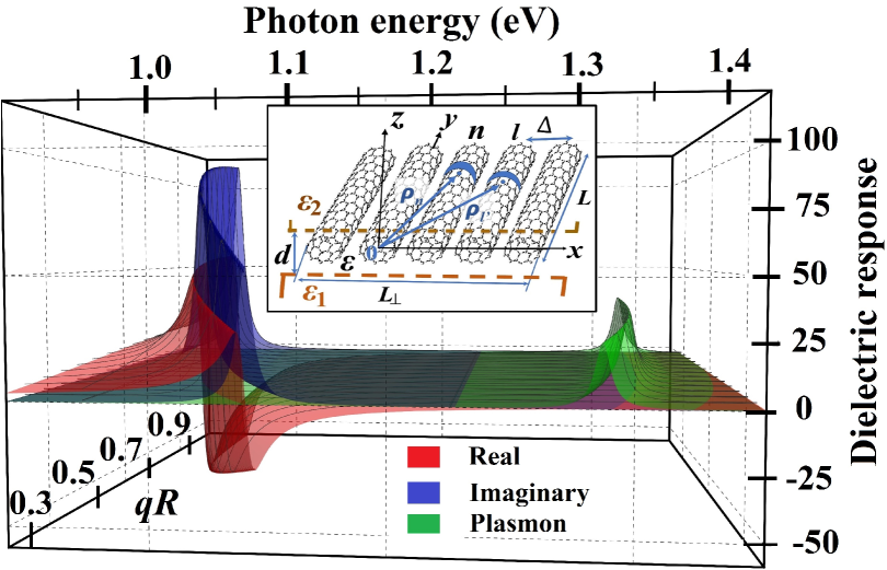
One can see from Eq. (1) that if , then . Therefore, the longitudinal component becomes equal to the transverse component of the CN array dielectric tensor in this limit, turning the CN film into an isotropic dielectric film. This behavior of the dielectric tensor of the CN array as approaches to zero is consistent with that of a film of metallic cylinders discussed in Ref. Bo2019ME . Figure 1 shows the dielectric responses for an ultrathin (10,0) CN film of thickness and intertube distance , calculated from Eq. (1). We consider the host dielectric medium of permittivity , surrounded by air (). For and the fractional density for a homogeneous SWCN array is , which is less than half of its the maximum possible value, indicating the presence of a significant dielectric screening effect. The red colored surface presents the refraction band defined by , the blue colored surface depicts the exciton absorption resonance given by , and the green colored surface shows the interband plasmon response defined as , all plotted in the neighborhood of the first single-tube exciton resonance. Due to screening and spatial dispersion, in the homogeneous SWCN film the plasmon resonance is positioned much closer in energy to the exciton resonance than it occurs in an individual isolated SWCN (cf. Fig. 2, inset).
III Thermal Average of Dielectric Response
To obtain the -dependence of the CN array longitudinal dielectric response in Eq. (1), the thermal averaging can be done as follows
| (2) |
Here, the -space population distribution function is of the form AdBo_PR2020
| (3) |
with representing the excitation energy of the CN array collective eigen-state produced by a single-tube -subband exciton with the energy due to the intertube dipole-dipole interaction coupling , and
| (4) |
to provide the proper normalization .
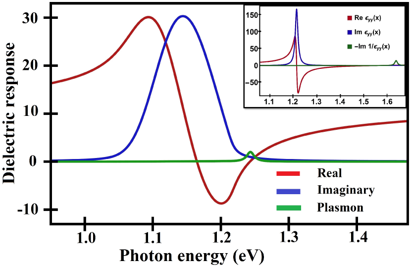
Figure 2 shows the thermally averaged functions , and for the CN film made up of a periodic array of the (10,0) CNs. The functions are calculated numerically as given by Eqs. (1)-(4) for K and the same array parameters as those used in Fig. 1. The inset in Fig. 2 shows the dielectric responses of the individual (10,0) CN in the same energy range for comparison. The (10,0) CN shows sharp, narrow and intense resonance peaks, quite different from the thermally broaden resonances of the (10,0) CN array. For a single CN, the plasmon peak is positioned far away from the exciton peak. In the array of nanotubes they are spaced much closer together. The interaction among the CNs and the thermal broadening effect bring the exciton and plasmon response functions closer to each other.
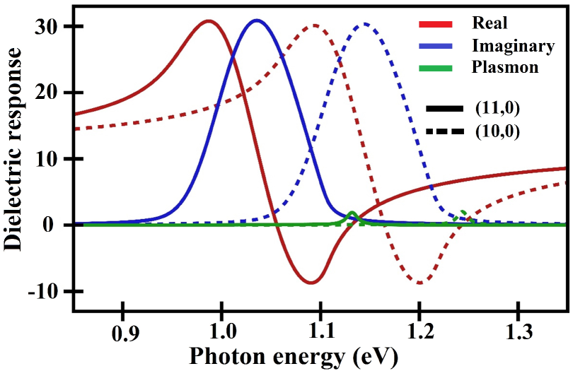
Figure 3 compares the thermally averaged (300 K) dielectric response functions for the ultrathin (10,0) and (11,0) CN arrays, calculated from Eqs. (1)-(4) with the same array parameters as before. For both arrays the exciton and plasmon resonance peaks are situated some energy apart. However, an interesting feature here is that the plasmon peak of the (11,0) CN array is almost exactly in resonance with the exciton absorption peak of the (10,0) CN array, whereby a strong exciton-plasmon coupling should be possible in an inhomogeneous densely packed mixture of these two SWCN arrays.
To obtain the dielectric response functions for an inhomogeneous CN film composed of non-identical homogeneous SWCN arrays, the Maxwell-Garnett (MG) mixing method can be used Ma2016 , to give the effective dielectric response of the -component mixture in the form
| (5) |
Here, is the thermally averaged dielectric response of the -th homogeneous CN array component and is its relative weight within the -component mixture, . The MG-mixing of the homogeneous SWCN arrays leads to an additional inhomogeneous broadening of the exciton and plasmon resonances in the CN array mixture AdBo_MA2020 . We do believe that the broad CN film dielectric response spectra reported in Ref. RoEtal2019 come mostly from the inhomogeneous broadening. For a properly fabricated SWCN array mixture, these broadened exciton and plasmon resonances can overlap as it occurs for the (10,0)/(11,0) CN array mixture shown in Fig. 3, thereby making the exciton-plasmon coupling to strongly affect the optical properties of a composite film.
IV Lineshape and Rabi-Splitting
Previously, the exciton absorption lineshape under the exciton-plasmon coupling was analyzed for individual CNs and composite CN materials in Refs. BoWoTa2009 ; Bo2011 ; NiEtAl2010 ; ChEtAl2017 . We here use the approach of Ref. BoWoTa2009 for a properly tuned mixture of the two ultrathin homogeneous arrays of the (10,0) and (11,0) CNs. We mix these arrays using Eq. (5), in which we have , where and are the relative weights of the thermally averaged (10,0) and (11,0) CN arrays, respectively. We focus on the energy range in the neighborhood of the first exciton absorption resonance of the (10,0) CN array. As was mentioned above and is shown in Fig. 3, the interband plasmon resonance of the (11,0) CN array is almost exactly in resonance with the exciton absorption resonance of the (10,0) CN array, whereas the (10,0) CN array plasmon peak is positioned pretty much aside at higher energy and out of resonance with its own exciton absorption peak. Under these conditions, in the mixture of the two arrays the lineshape profile of the first exciton absorption resonance of the (10,0) CN array takes the form BoWoTa2009
| (6) |
Here, all quantities are dimensionless, i.e., normalized by to match Eq. (1) so that , , and the condition is assumed to hold BoWoTa2009 , which is indeed the case for the MG mixture we consider. Other notations are , is the exciton spontaneous decay rate into plasmons, is the Rabi-splitting parameter, is the half-width-at-half-maximum of the plasmon resonance with the energy , and is an additional exciton energy broadening (normally attributed to the exciton-phonon relaxation for which we use fs, a nominal scattering time).
We mix these CN arrays at different weight combinations. From the room-temperature response functions and of each mixture we determine the exact exciton and interband plasmon resonance positions, and respectively, as well as their respective intensities and the half-width-at-half-maxima and to be plugged in Eq. (6) to obtain the lineshape profile for the respective mixture of the (10,0) and (11,0) CN arrays forming the composite film. Furthermore, since only excitons are produced in optical dipole transitions stimulated by the transversely polarized electromagnetic (light) radiation, while plasmons require longitudinally polarized electromagnetic waves (electron beam) to be excited, the optical absorption is due to excitons only even though they might be mixed with plasmons to result in an absorption lineshape profile (Rabi) splitting. In view of this, the equal intensities of the split resonances in Eq. (6) should be corrected by the respective exciton and plasmon fractions, which are different from if the exciton and plasmon resonance positions do not coincide exactly. More specifically, the exciton fraction is given by Bo_OE_2015
| (7) |
where , and the plasmon fraction is , respectively. The split resonances of Eq. (6) should be multiplied by their respective fractions according to Eq. (7).
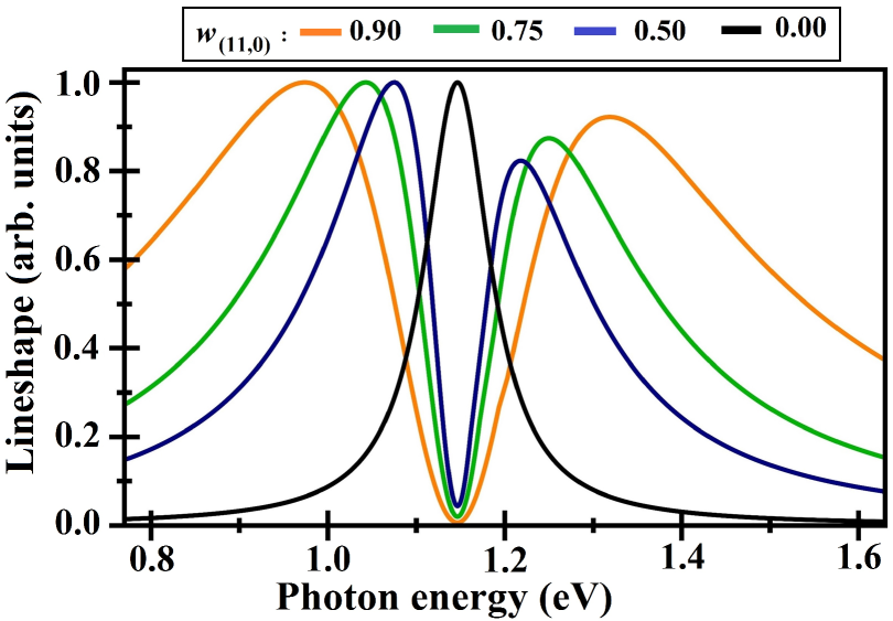
Figure 4 shows the absorption lineshape profiles of the first exciton absorption resonance of the (10,0) CN array calculated using Eqs. (6) and (7) for four different relative weight combinations of the (10,0) and (11,0) CN arrays in the MG mixture of the same material and geometry parameters as before. All profiles exhibit the line-splitting (aka Rabi-splitting), which is a signature of the strong exciton-plasmon coupling BoWoTa2009 . The lineshapes are normalized by the largest peak intensity. As the relative weight of the (11,0) CN-array increases, the split peak intensities tend to become even. The larger weight of the (11,0) CN-array also results in an increased broadening and a greater splitting of the entire absorption profile. This splitting quickly decreases with the reduction of the (11,0) CN-array relative weight, to eventually turn into a single-peak resonance absorption profile for zero relative weight of the (11,0) CN-array in the mixture.
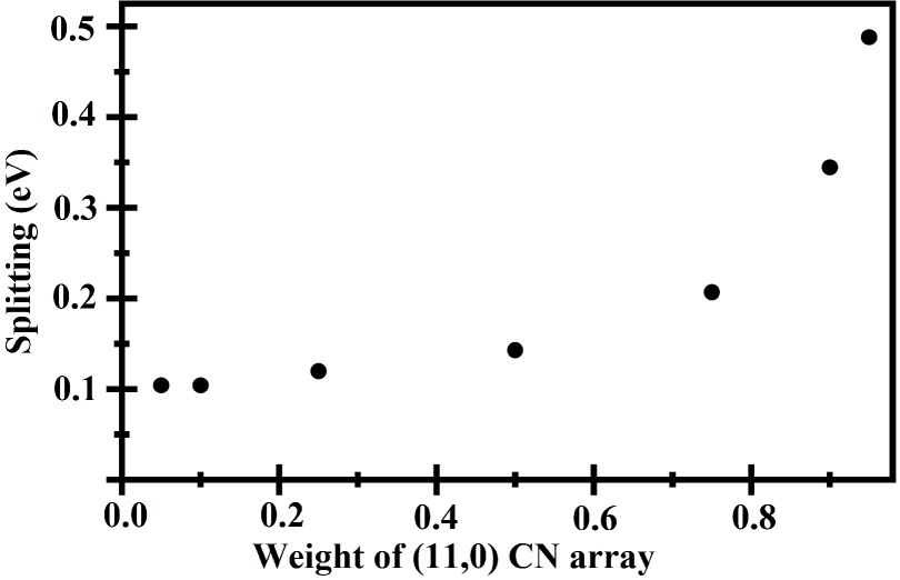
Figure 5 shows the Rabi-splitting itself of Fig. 4, computed and plotted as a function of the (11,0) CN-array component relative weight. The absorption profile Rabi-splitting of the composite film can be seen to increase with the relative weight of the (11,0) CN-array, thus reflecting the increasing role of the plasmon contribution in the MG mixture. The dependence is not a linear one though; for it goes abruptly up. One can see the variation of the characteristic exciton absorption line splitting in the range of eV in our case, which is as large as the typical exciton binding energies ( eV Pe2004 ; Ped2003 ; Ca2006 ; WaEtal2005 ) of individual small-diameter semiconducting CNs. The larger Rabi-splitting indicates the stronger exciton-plasmon coupling and the decreased light absorption, accordingly, in the energy window in-between the split resonance absorption peaks. Therefore, by varying the relative weights of the two array components one can tune the exciton-plasmon coupling and thereby the optical absorption profile of the composite film, to make the film transmit or absorb light in the neighborhood of an exciton absorption resonance on-demand. A very similar effect was recently demonstrated theoretically for double-wall CNs BoPo2017 where the exciton-plasmon coupling was proposed to control the exciton Bose condensation effect in properly selected double-wall CN systems.
V Summary and Conclusions
In this contribution, we study theoretically the electromagnetic response for an experimentally feasible CN film system composed of periodic arrays of parallel aligned semiconducting SWCNs embedded in an ultrathin finite-thickness dielectric layer. Our main focus is the exciton-plasmon interactions and we show how the exciton-plasmon coupling can be controlled by adjusting the intrinsic parameters of the system. We evaluate the in-plane dynamical dielectric response functions along the CN alignment direction using the low-energy plasmonic response calculation technique Bo2019ME combined with the many-particle Green’s function formalism Mahan2000 . The expression we obtain accounts for the intertube dipole-dipole interaction and links the response of the CN film to the complex axial conductivity of an individual constituent SWCN, an active component of the composite ultrathin film. The individual SWCN conductivity can be calculated using the -method of the CN-band structure theory Ando2005 . The overall response of the system can be controlled by its intrinsic collective parameters such as SWCN volume fraction and dielectric permittivities of materials involved, in addition to the individual constituent SWCN conductivity. The CN fraction depends not only on the CN density but also on the thickness of the dielectric layer.
We also study the thermal broadening and inhomogeneity effects for the CN film dielectric response functions to understand the optical properties of realistic experimental systems at room temperature. For homogeneous single-CN films, the intertube coupling and thermal broadening bring the exciton and plasmon resonances closer together. They can even overlap due to the inhomogeneous broadening for films composed of array mixtures with a slight CN diameter distribution. In such systems the real part of the dielectric response function is negative for a sufficiently broad range of the incident photon energy (negative refraction band), and the CN film behaves as a hyperbolic metamaterial. This explains the experimental observations reported recently for horizontally aligned finite-thickness quasi-homogeneous CN films RoEtal2019 . Using the MG mixing method Ma2016 , we show that for a properly fabricated two-component inhomogeneous SWCN film the broadened exciton and plasmon resonances can overlap in a way it occurs for the (10,0)/(11,0) CN array mixture which we here simulate as an example. In such systems the strong exciton-plasmon coupling and associated hybridization result in the Rabi-splitting of the exciton absorption lineshape profile, thereby strongly affecting the optical response of the two-component composite film. We show that by varying the relative weights of the two array components one can tune the optical absorption profile to make the film transmit or absorb light in the neighborhood of an exciton absorption resonance on-demand.
Acknowledgements.
This research is supported by the U.S. National Science Foundation under Condensed Matter Theory Program Award No. DMR-1830874 (I.V.B.)Data Availability: The data that supports the findings of this study are available within the article.
References
- (1) I. V. Bondarev, “Surface electromagnetic phenomena in pristine and atomically doped carbon nanotubes,” J. Comput. Theor. Nanosci. 7, 1673 (2009).
- (2) A. Martinez and S. Yamashita, “Carbon nanotube-based photonic devices: Applications in nonlinear optics,” in Carbon Nanotubes, edited by J. M. Marulanda (IntechOpen, Rijeka, 2011).
- (3) M. F. D. Volder, S. H. Tawfick, R. H. Baughman, and A. Hart, “Carbon nanotubes: present and future commercial applications,” Science 339, 535 (2013).
- (4) P. Avouris, M. Freitag, and V. Perebeinos, “Carbon-nanotube photonics and optoelectronics,” Nature Photon 2, 341 (2008).
- (5) M.-Y. Wu, J. Zhao, N. J. Curley, T.-H. Chang, Z. Ma, and M. S. Arnold, “Biaxially stretchable carbon nanotube transistors,” J. Appl. Phys 122, 124901 (2017).
- (6) J. A. Roberts, S. J. Yu, P. H. Ho, S. Schoeche, A. L. Falk, and J. A. Fan, “Tunable hyperbolic metamaterials based on self-assembled carbon nanotubes,” Nano Lett. 19, 3131 (2019).
- (7) T. Hertel and I. V. Bondarev, “Photophysics of carbon nanotubes and nanotube composites,” Chem. Phys. 413, 1 (2013).
- (8) S. Zhu, J. Ni, and Y. Li, “Carbon nanotube-based electrodes for flexible supercapacitors,” Nano Res. 13, 1815 (2020).
- (9) A. L. Falk, K.-C. Chiu, D. B. Farmer, Q. Cao, J. Tersoff, Y.-H. Lee, P. Avouris, and S.-J. Han, “Coherent plasmon and phonon-plasmon resonances in carbon nanotubes,” Phys. Rev. Lett. 118, 257401 (2017).
- (10) P.-H. Ho, D. B. Farmer, G. S. Tulevski, S.-J. Han, D. M. Bishop, L. M. Gignac, J. Bucchignano, P. Avouris, and A. L. Falk, “Intrinsically ultrastrong plasmon-exciton interactions in crystallized films of carbon nanotubes,” Proceedings of the National Academy of Sciences 115, 12662 (2018).
- (11) K.-C. Chiu, A. L. Falk, P.-H. Ho, D. B. Farmer, G. Tulevski, Y.-H. Lee, P. Avouris, and S.-J. Han, “Strong and broadly tunable plasmon resonances in thick films of aligned carbon nanotubes,” Nano Lett. 17, 5641 (2017).
- (12) V. A. Markel, “Introduction to the maxwell garnett approximation: tutorial,” J. Opt. Soc. Am. A 33, 1244 (2016).
- (13) G. D. Mahan, Many-particle physics, 3rd ed. (Kluwer Academic, New York, 2000).
- (14) C. M. Adhikari and I. V. Bondarev, “Optical response of ultrathin periodically aligned single-wall carbon nanotube films,” MRS Advances, pp. 1-7 (2020) (DOI: 10.1557/adv.2020.234).
- (15) I. V. Bondarev, “Finite-thickness effects in plasmonic films with periodic cylindrical anisotropy [Invited],” Opt. Mater. Express 9, 285 (2019).
- (16) L. V. Keldysh, “Coulomb interaction in thin semiconductor and semimetal films,” Soviet Journal of Experimental and Theoretical Physics Letters 29, 658 (1979).
- (17) I. V. Bondarev and V. M. Shalaev, “Universal features of the optical properties of ultrathin plasmonic films,” Opt. Mater. Express 7, 3731 (2017).
- (18) I. V. Bondarev, H. Mousavi, and V. M. Shalaev, “Optical response of finitethickness ultrathin plasmonic films,” MRS Communications 8, 1092 (2018).
- (19) I. V. Bondarev, H. Mousavi, and V. M. Shalaev, “Transdimentional epsilon-near-zero modes in planar plasmonic nanostructures,” Phys. Rev. Research 2, 013070 (2020).
- (20) T. Ando, “Theory of electronic states and transport in carbon nanotubes,” J. Phys. Soc. Jpn 74, 777 (2005).
- (21) J. Bellessa, C. Bonnand, J. C. Plenet, and J. Mugnier, “Strong coupling between surface plasmons and excitons in an organic semiconductor,” Phys. Rev. Lett. 93, 036404 (2004).
- (22) A. E. Schlather, N. Large, A. S. Urban, P. Nordlander, and N. J. Halas, “Near-field mediated plexcitonic coupling and giant rabi splitting in individual metallic dimers,” Nano Lett. 13, 3281 (2013).
- (23) A. Manjavacas, F. J. Garcia de Abajo, and P. Nordlander, “Quantum plexcitonics: Strongly interacting plasmons and excitons,” Nano Lett. 11, 2318 (2011).
- (24) Y. Fedutik, V. V. Temnov, O. Schöps, U. Woggon, and M. V. Artemyev, “Exciton-plasmon-photon conversion in plasmonic nanostructures,” Phys. Rev. Lett. 99, 136802 (2007).
- (25) D. Dai, Z. Dong, and J. Fan, “Giant photoluminescence enhancement in SiC nanocrystals by resonant semiconductor exciton–metal surface plasmon coupling,” Nanotechnology 24, 025201 (2012).
- (26) P. Vasa, R. Pomraenke, S. Schwieger, Y. I. Mazur, V. Kunets, P. Srinivasan, E. Johnson, J. E. Kihm, D. S. Kim, E. Runge, G. Salamo, and C. Lienau, “Coherent exciton–surface-plasmon-polariton interaction in hybrid metalsemiconductor nanostructures,” Phys. Rev. Lett. 101, 116801 (2008).
- (27) G. A. Wurtz, P. R. Evans, W. Hendren, R. Atkinson, W. Dickson, R. J. Pollard, A. V. Zayats, W. Harrison, and C. Bower, “Molecular plasmonics with tunable exciton–plasmon coupling strength in j-aggregate hybridized au nanorod assemblies,” Nano Lett. 7, 1297 (2007).
- (28) N. Asgari and S. M. Hamidi, “Exciton-plasmon coupling in 2D plexitonic nanograting,” Opt. Mater. 81, 45 (2018).
- (29) I. V. Bondarev, L. M. Woods, and A. Popescu, “Exciton-plasmon interactions in individual carbon nanotubes,” (Nova Science, NY, 2011).
- (30) I. V. Bondarev, K. Tatur, and L. M.Woods, “Surface exciton-plasmons and optical response of small-diameter carbon nanotubes,” Opt. Spectrosc. 108, 376 (2010).
- (31) I. V. Bondarev, K. Tatur, and L. M. Woods, “Optical response of small-diameter semiconducting carbon nanotubes under exciton–surface-plasmon coupling,” Optics Communications 282, 661 (2009).
- (32) I. V. Bondarev, L. M. Woods, and K. Tatur, “Strong exciton-plasmon coupling in semiconducting carbon nanotubes,” Phys. Rev. B 80, 085407 (2009).
- (33) I. V. Bondarev and T. Antonijevic, “Surface plasmon amplification under controlled exciton-plasmon coupling in individual carbon nanotubes,” Phys. Stat. Sol. C 9, 1259 (2012).
- (34) I. V. Bondarev, “Single-wall carbon nanotubes as coherent plasmon generators,” Phys. Rev. B 85, 035448 (2012).
- (35) I. V. Bondarev and P. Lambin, “Vacuum-field rabi oscillations in atomically doped carbon nanotubes,” Phys. Lett. A 328, 235 (2004).
- (36) I. V. Bondarev and A. V. Meliksetyan, “Possibility for exciton bose-einstein condensation in carbon nanotubes,” Phys. Rev. B 89, 045414 (2014).
- (37) I. V. Bondarev and A. Popescu, “Exciton Bose-Einstein condensation in double walled carbon nanotubes,” MRS Advances, 2, 2401 (2017) (DOI: 10.1557/adv.201.435).
- (38) W. Zhang, A. O. Govorov, and G. W. Bryant, “Semiconductor-metal nanoparticle molecules: Hybrid excitons and the nonlinear fano effect,” Phys. Rev. Lett. 97, 146804 (2006).
- (39) A. M. Dibos, Y. Zhou, L. A. Jauregui, G. Scuri, D. S. Wild, A. A. High, T. Taniguchi, K. Watanabe, M. D. Lukin, P. Kim, and H. Park, “Electrically tunable exciton–plasmon coupling in a WSe2 monolayer embedded in a plasmonic crystal cavity,” Nano Lett. 19, 3543 (2019).
- (40) E. Cao, W. Lin, M. Sun, W. Liang, and Y. Song, “Exciton-plasmon coupling interactions: from principle to applications,” Nanophotonics 7, 59 (2018).
- (41) C. M. Adhikari and I. V. Bondarev, “Collective excitations and optical response of ultrathin carbon nanotube arrays,” 2020 (to be published).
- (42) I. V. Bondarev and P. Lambin, “van der waals coupling in atomically doped carbon nanotubes,” Phys. Rev. B 72, 035451 (2005).
- (43) I. V. Bondarev, “Asymptotic exchange coupling of quasi-one-dimensional excitons in carbon nanotubes,” Phys. Rev. B 83, 153409 (2011).
- (44) A. E. Nikolaenko, F. De Angelis, S. A. Boden, N. Papasimakis, P. Ashburn, E. Di Fabrizio, and N. I. Zheludev, “Carbon nanotubes in a photonic metamaterial,” Phys. Rev. Lett. 104, 153902 (2010).
- (45) K.-C. Chiu, A. L. Falk, P.-H. Ho, D. B. Farmer, G. Tulevski, Y.-H. Lee, P. Avouris, and S.-J. Han, “Strong and broadly tunable plasmon resonances in thick films of aligned carbon nanotubes,” Nano Lett. 17, 5641 (2017).
- (46) I. V. Bondarev, “Plasmon enhanced raman scattering effect for an atom near a carbon nanotube,” Opt. Express 23, 3971 (2015).
- (47) T. G. Pedersen, “Exciton effects in carbon nanotubes,” Carbon 42, 1007 (2004).
- (48) T. G. Pedersen, “Variational approach to excitons in carbon nanotubes,” Phys. Rev. B 67 (2003).
- (49) R. B. Capaz, C. D. Spataru, S. Ismail-Beigi, and S. G. Louie, “Diameter and chirality dependence of exciton properties in carbon nanotubes,” Phys. Rev. B 74 (2006).
- (50) F.Wang, “The optical resonances in carbon nanotubes arise from excitons,” Science 308, 838 (2005).