A model for atomic precision p-type doping with diborane on Si(100)-21
Abstract
Diborane (B2H6) is a promising molecular precursor for atomic precision p-type doping of silicon that has recently been experimentally demonstrated [T. Škereň, et al., Nature Electronics (2020)]. We use density functional theory (DFT) calculations to determine the reaction pathway for diborane dissociating into a species that will incorporate as electrically active substitutional boron after adsorbing onto the Si(100)-21 surface. Our calculations indicate that diborane must overcome an energy barrier to adsorb, explaining the experimentally observed low sticking coefficient ( at room temperature) and suggesting that heating can be used to increase the adsorption rate. Upon sticking, diborane has an chance of splitting into two BH3 fragments versus merely losing hydrogen to form a dimer such as B2H4. As boron dimers are likely electrically inactive, whether this latter reaction occurs is shown to be predictive of the incorporation rate. The dissociation process proceeds with significant energy barriers, necessitating the use of high temperatures for incorporation. Using the barriers calculated from DFT, we parameterize a Kinetic Monte Carlo model that predicts the incorporation statistics of boron as a function of the initial depassivation geometry, dose, and anneal temperature. Our results suggest that the dimer nature of diborane inherently limits its doping density as an acceptor precursor, and furthermore that heating the boron dimers to split before exposure to silicon can lead to poor selectivity on hydrogen and halogen resists. This suggests that while diborane works as an atomic precision acceptor precursor, other non-dimerized acceptor precursors may lead to higher incorporation rates at lower temperatures.
Sandia National Laboratories]Center for Computing Research, Sandia National Laboratories, Albuquerque NM 87185 Sandia National Laboratories] Sandia National Laboratories, Albuquerque NM 87185 Sandia National Laboratories]Center for Computing Research, Sandia National Laboratories, Albuquerque NM 87185 Sandia National Laboratories] Sandia National Laboratories, Albuquerque NM 87185
![[Uncaptioned image]](/html/2010.00129/assets/x1.png)
1 Introduction
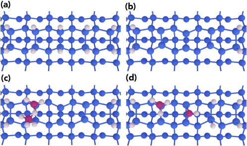
Atomic precision advanced manufacturing (APAM) promises to greatly improve capabilities for nanoelectronic device design, with the potential for realizing exotic quantum and classical devices that require a high-level of precision in the placement of dopants within silicon and/or dopant densities beyond the solid-solubility limit. 1 APAM begins with a Si(100)-21 surface that is terminated with a single monolayer of resist atoms. Most prominently, a monohydride termination (see Figs. 1a) has been used, but halogen resists are an active area of research as well. 2, 3, 4 A tool such as a Scanning Tunneling Microscope (STM)5 or a pulsed UV laser 6 is then used to selectively remove the resist atoms from a region of interest (see Figs. 1b), after which the surface is exposed to a precursor molecule containing the desired dopant atom. The precursor gas selectively adsorbs onto the bare silicon as opposed to the surrounding resist (see Figs. 1c) and, through a series of chemical reactions, leads to a bridging configuration (see Figs. 1d) that will eventually lead to an incorporated dopant atom. For a phosphine (PH3) precursor gas, a phosphorus donor atom can be placed onto a silicon surface to within one lattice site of a particular target. 7
While chemistries for atomic precision placement of donors have been well-developed both theoretically and experimentally,7, 8, 9, 10, 11, 2, 12, 13 less work has been done in developing a similar chemistry for atomic precision acceptor placement. However, such an advance is essential to developing processes that would enable the creation of acceptor-based quantum devices, p-n junctions, or more general integration with standard CMOS electronics.14, 15, 16, 17 Among the key choices that need to be made are the chemical composition of the resist and the precursor molecule that reacts with the exposed surface to yield an atom that can incorporate in an electrically active configuration. The precursor molecule for acceptor doping should selectively adsorb onto bare silicon relative to the resist and decompose into an incorporated acceptor atom with the addition of only a small amount of thermal energy. Diborane (B2H6) was recently demonstrated for p-type -doping with a monohydride resist, serving as a relatively simple precursor for boron incorporation analogous to phosphine for phosphorus. 17
In this paper, we theoretically study diborane as an APAM acceptor precursor on Si(100)-21 with both a hydrogen resist, given its established selectivity for phosphine, and a chlorine resist, due to recent interest.3, 4 We use Density Functional Theory (DFT) to calculate the reaction pathway for diborane decomposition on silicon surfaces, along with reaction barriers associated with moving between different configurations. We then utilize these reaction barriers and configurations in a Kinetic Monte Carlo (KMC) model that predicts the geometry and rate of incorporation. We consider both small windows in the resist intended to incorporate one or a few boron atoms, as well as larger windows up to tens of nanometers wide. By assuming that substitutional dimerized boron will be electrically inactive, we are able to reproduce incorporation rates consistent with experiment. This leads us to conclude that the dimer nature of diborane limits its performance compared to the analogous, non-dimerized phosphine precursor.
2 Methods
2.1 Electronic Structure Calculations
We determine the thermodynamic adsorption energy of any particular configuration with the following equation:
| (1) |
where is the adsorption energy of the molecule on the silicon surface, is the total energy of the adsorbate on the slab, is the total energy of the slab without any adsorbate, and is the total energy of the isolated molecule. Negative values of therefore imply a thermodynamically favorable adsorption energy for that configuration. All total energy calculations are performed using the plane wave quantum-espresso software package.18 To compute reaction barriers between configurations we use the Nudged Elastic Band (NEB) method, also implemented in quantum-espresso. We use norm-conserving pseudopotentials from the PseudoDojo repository 19 and the Perdew-Burke-Ernzerhof exchange correlation functional. 20 We use kinetic energy cutoffs of 50 Ry and 200 Ry for the plane wave basis sets used to describe the Kohn-Sham orbitals and charge density, respectively. We use a 221 Monkhorst-Pack grid to sample the Brillioun zone.21
We perform all adsorption energy calculations on the 44 supercell of a seven-layer thick Si(100)-2x1 slab with a 20 Å vacuum region. We place a hydrogen resist on the surface with the exception of three dimer sites, allowing us to gauge the selectivity of the diborane molecules on a bare silicon surface versus a resist-terminated surface. On the other end of the slab, the dangling bonds of the silicon are passivated with selenium atoms to prevent spurious surface effects. Selenium was determined to be optimal for achieving this purpose with minimal strain. The bottom four layers of the slab are frozen and the geometry of the surface layers along with the adsorbate are relaxed until the interatomic forces are lower than 50 meV/Å. We compute the reference molecular energy for a single diborane molecule in a 15 Å3 box.
2.2 Kinetic Monte Carlo
We then use a Kinetic Monte Carlo (KMC) model 22, 23 implemented using the KMCLib software package 24 to predict the incorporation rate of boron atoms in patches of exposed silicon that can be several nanometers wide. Our KMC uses transition rates based on the Arrhenius equation , 25 where is transition rate, is the attempt frequency, is the reaction barrier found from our earlier DFT calculations, is the Boltzmann constant, and is the temperature. We set all attempt frequencies to s-1 as a reasonable order of magnitude estimate based on an analysis of attempt frequencies for the dissociation of phosphine on silicon.11 We could use the Vineyard equation to compute more precise attempt frequencies within DFT, but given the simplicity of the pathway that we propose and the relatively low level of accuracy of the barrier height calculations, a simple estimate suffices to study the qualitative aspects of the incorporation chemistry. Unless otherwise noted, we follow the incorporation schedule layed out by Škereň and coworkers,17 utilizing a dosing pressure of 1.5 10-7 Torr for 10 minutes at , followed by an anneal at for 1 minute.
We repeat each KMC calculation 200 times to obtain a meaningful statistical sampling of likely outcomes and report the average outcomes, along with standard deviations as applicable. We calculate the standard error by assuming a Poisson distribution of measured counts and using the standard error based on sample size.
3 Results
3.1 Reaction Pathway
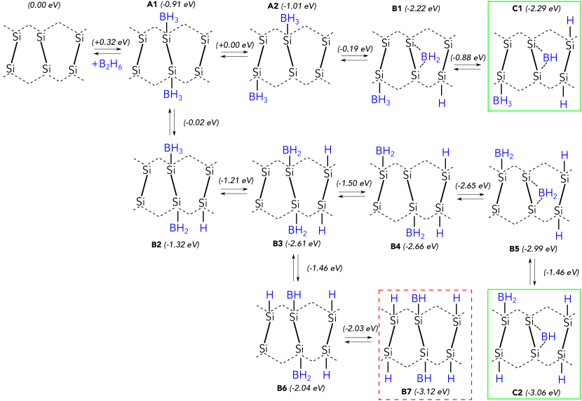
The reaction pathway of diborane on a silicon surface was determined using DFT, with the lowest energy configurations shown in Fig. 2. For ease of reference, we adopt a similar naming convention to the one developed by Wilson et al. 8 Structures labeled with an A consist entirely of BH3 fragments, structures labeled with a B consist of BH2 fragments, and finally structures labeled with a C have bridging BH fragments.
We predict diborane requires overcoming an energy barrier to adsorb into the lowest thermodynamic energy configuration, explaining the experimental observation that diborane has a low sticking coefficient () at room temperature.26, 27 The lowest energy adsorption site for diborane on silicon requires a partial dissociation of the diborane molecule into two BH3 fragments, each sitting on an opposite end of the dimer (configuration A1). This dissociation requires overcoming a reaction barrier of 0.32 eV to achieve an adsorption energy of –0.91 eV. While the ultimate thermodynamic stability of this adsorption is comparable to the reported –0.7 eV adsorption energy of phosphine,11 the addition of the reaction barrier implies that unless energy is provided to begin the dissociation process, diborane will not stick to the silicon surface. In contrast, on a hydrogen resist, diborane only weakly physisorbs with an adsorption energy of –0.02 eV and does not dissociate. We thus predict that heating the surface will lead to significantly better adsorption onto bare silicon, as demonstrated by Škereň et al.17
The resulting pathway of the diborane fragments is then determined by whether the BH3 fragments start shedding hydrogen to nearby dimers or whether the BH3 fragments split to occupy different dimers. The pathway where diborane loses hydrogen to a nearby silicon dimer site (configuration B2) is more thermodynamically favorable with an adsorption energy of –1.32 eV as opposed to the configuration where the two BH3 fragments split (A2), which has an adsorption energy of –1.01 eV. The reaction barriers for each path are essentially identical, however, with the A1 to B2 reaction having a barrier of 0.89 eV as opposed to the 0.91 eV barrier of the A1 to A2 reaction. Both of these barriers are relatively high, requiring higher temperatures than the initial adsorption reaction. A molecule in the A1 configuration will therefore have an approximately equal chance of moving toward A2 or B2. This reaction defines the entire resulting path of the diborane molecule, fully illustrated in Fig. 2. For the sake of limiting our computation to a feasible subset of possible configurations and in analogy to similar work on phosphine dissociation,11, 28 we assume that once a diborane molecule reaches a bridging BH position, as in C1 and C2, it will eventually incorporate into the system.
In contrast, if the two boron atoms remain on the same dimer, as in the B7 configuration, we assume that they will incorporate into the silicon lattice as a dimerized B2 molecule which will likely be electrically inactive. This is substantiated by prior work on boron clustering in silicon in which electrically inactive complexes may rationalize the presence of immobile boron in studies on ion implanted samples. 29, 30, 31 Accordingly, the first step that limits the incorporation of electrically active boron is at A1, and whether the reaction proceeds to A2 or B2. The next step that determines electrically active incorporation is at B3, where a dimer with a BH2 molecule on both sides can either continue to lose hydrogen to a nearby dimer (B6), or split apart such that the BH2 molecules move to separate dimers (B4). This allows for non-dimerized bridging BH to form (C2).

The thermodynamic pathway for diborane dissociating and incorporating is entirely downhill, as shown in Fig. 3. Barriers remain high throughout the reaction process, however, with a dissociating molecule routinely having to overcome barriers on the order of 0.9 - 1.1 eV. The two incorporation reactions in particular, B1 to C1 and B5 to C2, have especially high barriers of 1.3 eV and 1.5 eV, respectively. These large reaction barriers necessitate high processing temperatures to result in significant numbers of incorporations. If we assume that an adsorbed diborane molecule will always take the lowest barrier option available to it, the molecule will eventually result in a bridging BH molecule in configuration C2. Two crucial configurations, however, A1 and B3, have two potential reactions with nearly identical reaction barriers, meaning molecules in these configurations will have nearly equal chances of which dissociation path they take, making the dissociation pathway of diborane highly stochastic.
3.2 Incorporation Rate
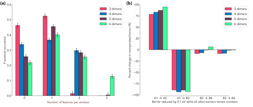
To understand the impact of this dissociation pathway stochasticity on the final incorporation rate of diborane, we parameterize a Kinetic Monte Carlo (KMC) model with the reaction barriers calculated from DFT and displayed in Fig. 3. We initially measure the incorporation rate of diborane in small windows of silicon that have been depassivated with the hope of incorporating a single acceptor within the space of a few lattice sites. As shown schematically in Fig. 2, a diborane molecule needs a space at least three dimers wide to have sufficient room for the boron dimer to split and to lose hydrogen. We therefore measure the number of boron incorporation events in three, four, five, and six dimer wide windows in Fig. 4a. For ease of discussion in the following section, we introduce the notation to describe the probability of acceptors incorporating into a -dimer wide window.
We find no dimer width that guarantees deterministic incorporation of a boron atom, although the probability of at least one incorporation event, does increase as a function of width . A three dimer wide window has the highest probability of a single acceptor incorporation with . This is lower than the equivalent probability of incorporation for a phosphine molecule, which has been experimentally measured at 0.7.32 This lowered probability can largely be attributed to the larger size of the diborane molecule, requiring several more steps for dissociation and splitting of the boron dimer than a phosphine molecule.
Because the rates in our KMC model are exponentially sensitive to barriers calculated using DFT, small changes in their values relative to the thermal energy can lead to changes in the final results of our analysis. For the temperatures relevant to our incorporation chemistry, the size of errors typical to DFT are sufficiently large that we should not take the quantitative predictions too seriously without considering the sensitivity of outcomes to errors (0.1 eV). Accordingly we need to focus on particular steps in the incorporation for which the molecule has two nearly equal barriers that it must choose between (e.g. configurations A1 and B3). Slightly favoring the A1 to A2 reaction by reducing the A1 to A2 barrier by merely 0.1 eV can increase the incorporation rate dramatically, leading to . In contrast, decreasing the A1 to B2 barrier by 0.1 eV, which favors the molecule losing hydrogen as opposed to splitting onto separate dimers, ensures virtually no incorporation with . In contrast, the B3 configuration is revealed to be a less important decision point in the dissociation of diborane: reducing either the B3 to B4 reaction or the B3 to B6 reaction by 0.1 eV leads to insignificant changes in incorporation levels. This can be attributed to the fact that the reverse reactions of note, B4 to B3 and B7 to B6, have relatively low reaction barriers (1.16 eV and 1.15 eV, respectively) compared to the incorporation reaction of interest B5 to C2 with a barrier of 1.53 eV. Thus a BH2 cluster in the B4 configuration is, in the end, slightly more likely to return to the B3 configuration than to fully incorporate as an electrically active dopant, reducing the impact of whether the BH2 molecules split to different dimer. This emphasizes the importance of the A1 configuration and the resulting splitting (or lack thereof) of the boron dimer to determining the ultimate incorporation levels of diborane. This suggests future theoretical work to focus on increasing the accuracy of energies for this configuration and the associated reaction barriers.
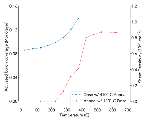
For -doping, the final incorporation level of boron into silicon is highly dependent on both the dose and anneal temperature, as demonstrated by simulations of larger 1010 nm depassivated systems. In Fig. 5, we predict the monolayer coverage and sheet density of activated dopants in a system after being dosed with diborane while independently altering the dose and anneal temperature. The incorporation rate increases with dose temperature, although not significantly until reaching . This can be attributed to the temperature becoming sufficiently high to activate the B1 to C1 reaction (with a barrier of 1.34 eV), which has a typical time scale (taken here as simply where is the Arrhenius rate of an equation) of 190 s at , but only 0.06 s at . Similarly, the B5 to C2 incorporation reaction becomes feasible only as temperatures increase with a typical reaction time scale of at and 0.03 s at . It is likely that the ability for diborane molecules to dissociate before the surface has become saturated with other molecules can lead to higher incorporation levels than seen in the anneal case, in which molecules often have to desorb or migrate before BH2 molecules have sufficient room to further dissociate. While temperatures during dosing should be limited to below at least to keep the hydrogen resist intact,17, 33 our analysis indicates that dose temperatures closer toward this limit may be an effective tactic for increased incorporation levels. In contrast, the system has essentially no incorporation for anneal temperatures below . At around , we predict that incorporation rates will begin to increase as a function of temperature until hitting a saturation point around , again likely due to activating the B1 to C1 and B5 to C2 reactions. At higher anneal temperatures, the activated sheet density remains largely constant.
Škereň et al., in contrast, find a drastic increase in sheet density of boron after , reaching a maximum of .17 They attribute this growth to the breaking apart of boron dimers from configurations such as B7, a process we notably do not model. At temperatures below , however, they measure an essentially constant sheet density of roughly , comparing favorably with the sheet density we predict at . This helps validate our assumption that bridging BH molecules are a reasonable proxy for final incorporation of a boron atom.
This incorporated sheet density of activated boron at anneal temperatures below is roughly half of the density that has been seen from the analogous phosphine process (),34 which can be achieved at considerably lower temperatures. This decrease in doping density can be directly attributed to the dimer nature of diborane. If we include boron atoms that end in a dimerized state (configuration B7 in Fig. 2) as activated boron atoms within our simulation, using just the dose and anneal, our predicted sheet density nearly triples to . The majority of boron deposited on the silicon surface by diborane, in fact, are therefore locked in electrically inactive configurations. The dimerization of boron atoms thus significantly decreases the maximal sheet density that can be achieved. While these dimerized boron atoms can be split apart by sufficient heating, it requires a significant amount of energy, occurring only at temperatures above . This thermal budget is undesirable and can lead to significant migration that degrades the precision nature of the doping process, particularly if the process is utilized in combination with a donor layer for complimentary logic.35
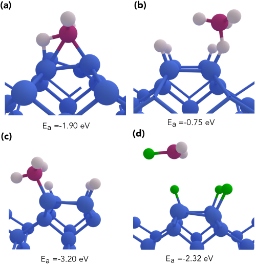
A conceivable alternative approach to increasing the final density of incorporated boron could be splitting diborane via heating into BHx fragments (here ) before exposing the resulting gas to silicon. While this would avoid the issue of seeding the surface with dimerized boron atoms that have a significant chance of remaining electrically inactive, we predict that the BHx fragments would have poor selectivity on bare silicon versus an atomic resist, ruining the atomic precision of dopant placement. In comparison to diborane, we predict BH3 has a much stronger adsorption energy on bare silicon of –1.9 eV, shown in Fig. 6a, matching the –1.86 eV reported by Konecny and Doren well.36 But BH3 also has a relatively high adsorption energy on a hydrogen resist of –0.75 eV, as shown in Fig. 6b. This indicates that while BH3 will preferentially adsorb onto bare silicon, if it lands on hydrogen it will fully chemisorb onto the surface. The selectivity picture is even worse for BH2: BH2 has an adsorption energy of –3.2 eV on a hydrogen resist, stripping the hydrogen from the surface to form a BH3 molecule that then directly attaches to the surface, as displayed in Fig. 6c. Furthermore, the selectivity woes of BH2 can not be mitigated by changing the atomic resist. For a chlorine resist, BH2 has an adsorption energy of –2.32 eV, stripping a chlorine atom from the resist to form BH2Cl, with a structure shown in Fig. 6d. This leaves a bare silicon site exposed for the next BHx fragment to directly attach to. The selectivity of BH2 on both hydrogen and chlorine is poor enough to make the splitting of diborane before exposure to silicon a likely non-viable option.
Overall, our results highlight how the dimer nature of diborane limits its capabilities as an APAM precursor. The final rate of dopant incorporation in small dimer windows is notably less than in phosphine and can be highly controlled by artificially increasing or decreasing the likelihood of diborane splitting into two BH3 molecules on separate dimers, revealing the importance of this split to final incorporation. The high reaction barriers of the diborane dissociation pathway force relatively high operating temperatures, and even at an anneal temperature of , diborane produces an activated sheet density that is half that seen in phosphine at lower temperatures. The incorporated sheet density triples when electrically inactive, dimerized boron atoms are counted, indicating that the majority of boron deposited on the surface is locked in an electrically inactive state. Furthermore, this problem cannot be easily overcome by heating to split the boron dimers, either before or after exposure to silicon. Our DFT calculations predict that splitting diborane into BHx fragments before exposure to silicon leads to a lack of selectivity with both hydrogen and chlorine resists, and Škereň et al. show that temperatures in excess of are required to split boron dimers once they have been adsorbed onto the silicon surface, a temperature that produces undesirable migration effects in the larger silicon device. This work therefore suggests that while diborane can work as an atomic precision acceptor precursor, it has inherent limitations. Alternative precursor molecules that do not naturally dimerize, such as BCl3, will likely yield improved APAM performance.
4 Conclusion
We have performed a detailed analysis of the dissociation pathway of diborane on the Si(100)-2x1 surface, calculating both adsorption energies and reaction barriers. We find that diborane must overcome a barrier to adsorb onto the bare silicon surface, explaining the experimentally observed need to heat the sample to achieve significant levels of diborane adsorption. We then used our dissociation pathway in a KMC model to determine incorporation statistics for both small and large windows in the resist. We demonstrate stochastic incorporation of an acceptor into silicon in resist windows between three and five dimers wide. This incorporation rate can be heavily influenced, however, by small errors in the calculation of the reaction barrier for the initial splitting of diborane onto two separate dimers or by the initial loss of hydrogen from one of the BH3 fragments. We then predict the temperature dependence of incorporation in larger depassivated windows. Due to the relatively high reaction barrier required for the development of a bridging BH molecule, elevated temperatures are favored in both the dose and anneal step of dissociation. We demonstrate that the dimer nature of diborane inherently limits its doping density in comparison to phosphine. Furthermore, splitting the diborane into BHx fragments before exposure to silicon is not a viable path as BH3 and BH2 exhibit poor selectivity for both hydrogen and chlorine resists. Our results highlight that the dimer nature of diborane inherently limits its potential as an acceptor precursor.
We gratefully acknowledge Rick Muller and Peter Schultz for useful discussions. This work was supported by the Laboratory Directed Research and Development program at Sandia National Laboratories under project 213017 (FAIR DEAL) and performed, in part, at the Center for Integrated Nanotechnologies, an Office of Science User Facility operated for the U.S. Deppartment of Energy (DOE) Office of Science. Sandia National Laboratories is a multi-mission laboratory managed and operated by National Technology and Engineering Solutions of Sandia, LLC, a wholly owned subsidiary of Honeywell International, Inc., for DOE’s National Nuclear Security Administration under contract DE-NA0003525. This paper describes objective technical results and analysis. Any subjective views or opinions that might be expressed in the paper do not necessarily represent the views of the U.S. Department of Energy or the United States Government.
| Numerical simulations | |
| Total Kernel Hours [] | 615100 |
| Thermal Design Power Per Kernel [] | 5.75 |
| Total Energy Consumption Simulations [] | 3536 |
| Average Emission Of CO2 | |
| In New Mexico, USA [] | 0.5644 |
| Total CO2-Emission For Numerical Simulations [] | 1996 |
| Were The Emissions Offset? | No |
| Transport | |
| Total CO2-Emission For Transport [] | 0 |
| Were The Emissions Offset? | n/a |
| Total CO2-Emission [] | 1996 |
References
- Ward et al. 2020 Ward, D. R.; Schmucker, S. W.; Anderson, E. M.; Bussmann, E.; Tracy, L.; Lu, T.-M.; Maurer, L. N.; Baczewski, A.; Campbell, D. M.; Marshall, M. T. et al. Atomic Precision Advanced Manufacturing for Digital Electronics. Electronic Device Failure Analysis 2020, 22, 4–11
- Pavlova et al. 2018 Pavlova, T. V.; Zhidomirov, G. M.; Eltsov, K. N. First-Principle Study of Phosphine Adsorption on Si (001)-2 1–Cl. The Journal of Physical Chemistry C 2018, 122, 1741–1745
- Dwyer et al. 2019 Dwyer, K. J.; Dreyer, M.; Butera, R. E. STM-Induced Desorption and Lithographic Patterning of Cl–Si (100)-(2 1). The Journal of Physical Chemistry A 2019, 123, 10793–10803
- Silva-Quinones et al. 2020 Silva-Quinones, D.; He, C.; Butera, R. E.; Wang, G. T.; Teplyakov, A. V. Reaction of BCl3 with H-and Cl-terminated Si (100) as a pathway for selective, monolayer doping through wet chemistry. Applied Surface Science 2020, 146907
- Lyding et al. 1994 Lyding, J.; Shen, T.-C.; Hubacek, J.; Tucker, J.; Abeln, G. Nanoscale patterning and oxidation of H-passivated Si (100)-2 1 surfaces with an ultrahigh vacuum scanning tunneling microscope. Applied physics letters 1994, 64, 2010–2012
- Katzenmeyer et al. 2020 Katzenmeyer, A.; Dmitrovic, S.; Baczewski, A.; Bussmann, E.; Lu, T.-M.; Anderson, E.; Schmucker, S.; Ivie, J.; Campbell, D.; Ward, D. et al. Photothermal alternative to device fabrication using atomic precision advanced manufacturing techniques. Novel Patterning Technologies for Semiconductors, MEMS/NEMS and MOEMS 2020. 2020; p 113240Z
- Schofield et al. 2003 Schofield, S. R.; Curson, N. J.; Simmons, M. Y.; Rueß, F. J.; Hallam, T.; Oberbeck, L.; Clark, R. G. Atomically precise placement of single dopants in si. Physical Review Letters 2003, 91, 136104
- Wilson et al. 2004 Wilson, H. F.; Warschkow, O.; Marks, N. A.; Schofield, S. R.; Curson, N. J.; Smith, P. V.; Radny, M. W.; McKenzie, D. R.; Simmons, M. Y. Phosphine Dissociation on the Si(001) Surface. Physical Review Letters 2004, 93, 226102
- Warschkow et al. 2005 Warschkow, O.; Wilson, H. F.; Marks, N. A.; Schofield, S. R.; Curson, N. J.; Smith, P. V.; Radny, M. W.; McKenzie, D. R.; Simmons, M. Y. Phosphine adsorption and dissociation on the Si(001) surface: An ab initio survey of structures. Physical Review B 2005, 72, 125328
- Wilson et al. 2006 Wilson, H. F.; Warschkow, O.; Marks, N. A.; Curson, N. J.; Schofield, S. R.; Reusch, T. C.; Radny, M. W.; Smith, P. V.; McKenzie, D. R.; Simmons, M. Y. Thermal dissociation and desorption of P H3 on Si(001): A reinterpretation of spectroscopic data. Physical Review B - Condensed Matter and Materials Physics 2006, 74, 1–10
- Warschkow et al. 2016 Warschkow, O.; Curson, N. J.; Schofield, S. R.; Marks, N. A.; Wilson, H. F.; Radny, M. W.; Smith, P. V.; Reusch, T. C.; McKenzie, D. R.; Simmons, M. Y. Reaction paths of phosphine dissociation on silicon (001). Journal of Chemical Physics 2016, 144, 014705
- Wyrick et al. 2019 Wyrick, J.; Wang, X.; Kashid, R. V.; Namboodiri, P.; Schmucker, S. W.; Hagmann, J. A.; Liu, K.; Stewart Jr, M. D.; Richter, C. A.; Bryant, G. W. et al. Atom-by-Atom Fabrication of Single and Few Dopant Quantum Devices. Advanced Functional Materials 2019, 29, 1903475
- Stock et al. 2020 Stock, T. J.; Warschkow, O.; Constantinou, P. C.; Li, J.; Fearn, S.; Crane, E.; Hofmann, E. V.; Kölker, A.; McKenzie, D. R.; Schofield, S. R. et al. Atomic-Scale Patterning of Arsenic in Silicon by Scanning Tunneling Microscopy. ACS nano 2020, 14, 3316–3327
- Shim and Tahan 2014 Shim, Y.-P.; Tahan, C. Bottom-up superconducting and Josephson junction devices inside a group-IV semiconductor. Nature communications 2014, 5, 1–8
- Van der Heijden et al. 2014 Van der Heijden, J.; Salfi, J.; Mol, J. A.; Verduijn, J.; Tettamanzi, G. C.; Hamilton, A. R.; Collaert, N.; Rogge, S. Probing the spin states of a single acceptor atom. Nano letters 2014, 14, 1492–1496
- Škereň et al. 2018 Škereň, T.; Pascher, N.; Garnier, A.; Reynaud, P.; Rolland, E.; Thuaire, A.; Widmer, D.; Jehl, X.; Fuhrer, A. CMOS platform for atomic-scale device fabrication. Nanotechnology 2018, 29, 435302
- Škereň et al. 2020 Škereň, T.; Köster, S. A.; Douhard, B.; Fleischmann, C.; Fuhrer, A. Bipolar device fabrication using a scanning tunnelling microscope. Nature Electronics 2020, 1–7
- Giannozzi et al. 2009 Giannozzi, P.; Baroni, S.; Bonini, N.; Calandra, M.; Car, R.; Cavazzoni, C.; Ceresoli, D.; Chiarotti, G. L.; Cococcioni, M.; Dabo, I. et al. QUANTUM ESPRESSO: a modular and open-source software project for quantum simulations of materials. Journal of Physics: Condensed Matter 2009, 21, 395502
- van Setten et al. 2018 van Setten, M. J.; Giantomassi, M.; Bousquet, E.; Verstraete, M. J.; Hamann, D. R.; Gonze, X.; Rignanese, G. M. The PSEUDODOJO: Training and grading a 85 element optimized norm-conserving pseudopotential table. Computer Physics Communications 2018, 226, 39–54
- Perdew et al. 1996 Perdew, J. P.; Burke, K.; Ernzerhof, M. Generalized Gradient Approximation Made Simple. Physical Review Letters 1996, 77, 3865–3868
- Monkhorst and Pack 1976 Monkhorst, H. J.; Pack, J. D. Special points for Brillouin-zone integrations. Physical review B 1976, 13, 5188
- Bortz et al. 1975 Bortz, A.; Kalos, M.; Lebowitz, J. A New Algorithm for Monte Carlo Simulation of Ising Spin Systems. Journal of Computational physics 1975, 17, 10–18
- Gillespie 1976 Gillespie, D. T. A general method for numerically simulating the stochastic time evolution of coupled chemical reactions. Journal of Computational Physics 1976, 22, 403–434
- Leetmaa and Skorodumova 2014 Leetmaa, M.; Skorodumova, N. V. KMCLib: A general framework for lattice kinetic Monte Carlo (KMC) simulations. Computer Physics Communications 2014, 185, 2340–2349
- Arrhenius 1889 Arrhenius, S. Uber die Reaktionsgeschwindigkeit bei der Inversion von Rohrzucker durch S auren. Zeitschrift für Physikalische Chemie 1889, 4, 226
- Yu et al. 1986 Yu, M. L.; Vitkavage, D.; Meyerson, B. Doping reaction of PH3 and B2H6 with Si (100). Journal of applied physics 1986, 59, 4032–4037
- Wang et al. 1996 Wang, Y.; Shan, J.; Hamers, R. J. Combined scanning tunneling microscopy and infrared spectroscopy study of the interaction of diborane with Si(001). Journal of Vacuum Science & Technology B: Microelectronics and Nanometer Structures Processing, Measurement, and Phenomena 1996, 14, 1038–1042
- Schofield et al. 2006 Schofield, S. R.; Curson, N. J.; Warschkow, O.; Marks, N. A.; Wilson, H. F.; Simmons, M. Y.; Smith, P. V.; Radny, M. W.; McKenzie, D. R.; Clark, R. G. Phosphine dissociation and diffusion on Si (001) observed at the atomic scale. The Journal of Physical Chemistry B 2006, 110, 3173–3179
- Tarnow 1992 Tarnow, E. Theory of two boron neutral pair defects in silicon. Journal of Physics: Condensed Matter 1992, 4, 5405
- Stolk et al. 1995 Stolk, P.; Gossmann, H.-J.; Eaglesham, D.; Poate, J. Implantation and transient boron diffusion: the role of the silicon self-interstitial. Nuclear Instruments and Methods in Physics Research Section B: Beam Interactions with Materials and Atoms 1995, 96, 187–195
- Zhu et al. 1996 Zhu, J.; Dela Rubia, T. D.; Yang, L.; Mailhiot, C.; Gilmer, G. H. Ab initio pseudopotential calculations of B diffusion and pairing in Si. Physical Review B 1996, 54, 4741
- Fuechsle 2011 Fuechsle, M. Precision Few-Electron Silicon Quantum Dots. Ph.D. thesis, 2011
- Oura et al. 1990 Oura, K.; Yamane, J.; Umezawa, K.; Naitoh, M.; Shoji, F.; Hanawa, T. Hydrogen adsorption on Si(100)-2x1 surfaces studied by elastic recoil detection analysis. Physical Review B 1990, 41, 1200
- Simmons et al. 2005 Simmons, M.; Ruess, F.; Goh, K.; Hallam, T.; Schofield, S.; Oberbeck, L.; Curson, N.; Hamilton, A.; Butcher, M.; Clark, R. et al. Scanning probe microscopy for silicon device fabrication. Molecular Simulation 2005, 31, 505–515
- Keizer et al. 2015 Keizer, J. G.; Koelling, S.; Koenraad, P. M.; Simmons, M. Y. Suppressing segregation in highly phosphorus doped silicon monolayers. ACS nano 2015, 9, 12537–12541
- Konecny and Doren 1997 Konecny, R.; Doren, D. Adsorption of BH3 on Si (100)-(2 1). The Journal of Physical Chemistry B 1997, 101, 10983–10985
- 37 Scientific CO2nduct. online, https://scientific-conduct.github.io