Diffusion-related lifetime of indirect excitons in diamond
Abstract
We investigate the lifetime of indirect excitons in extremely high purity diamond grown by the chemical vapor deposition method. A clear correlation is found between the lifetime and small strain (magnitude 10-4) assessed using birefringence, thanks to the effective absence of impurity traps. A surface recombination model, extended for nonradiative recombination at dislocations due to exciton diffusion, is proposed to explain the temperature-dependent lifetime. Based on the derived radiative lifetime, our model enables the prediction of lifetimes at any temperature as well as the highest achievable internal quantum efficiency of exciton luminescence in diamond, which can generally be applicable to a wide range of materials with high exciton binding energies.
- DOI
-
10.1103/
pacs:
Valid PACS appear hereIntroduction - The optical properties of wide bandgap semiconductors are generally characterized by excitons, i.e., pairs of an electron and a hole bound by the Coulomb force. This is contrary to conventional semiconductors, in which excitons have an effect at cryogenic temperatures only. Among various wide bandgap materials, diamond is a particularly robust solid-state platform for visible light emission from nitrogen-vacancy centers acting as a single photon source NV and for deep-ultraviolet (DUV) emission from excitons of intrinsic origin, which has been receiving increasing interest owing to sterilization applications effective at a shorter wavelength (235 nm) Makino than the limit of GaN-based blue light-emitting diodes (LEDs). In diamond, excitons are formed across the indirect bandgap (5.5 eV) and, due to their large binding energy, dominate the DUV emission up to room temperature.
So far, dynamics studies of optically excited carriers have mostly been performed using photoinduced transient grating (PITG) and time-resolved photoluminescence (TRPL) methods. Generally, transient carriers and excitons are subject to various complex pathways, such as trapping, diffusion, surface recombination PRAppl , and the radiative and nonradiative bulk recombinations. In 1996, a pioneering TRPL report by Takiyama et al. Takiyama clarified the temperature dependence of the bulk lifetime in moderate quality diamonds. The reductions of the lifetime at low and high temperatures were attributed to the trapping at impurities with the formation of bound excitons and to the exciton ionization, respectively. Although a reasonably long radiative lifetime, greater than 250 ns, was estimated, the derived activation energy for the bound excitons was in disagreement with the spectroscopic data, which has still not been clarified.
Over the two decades following the Takiyama report, with the advance of chemical-vapor-deposition (CVD) growth methods Balmer the purity of synthetic diamond has been dramatically improved. This motivated the review of the long-lasting question of using higher purity diamonds. Using PITG methods Kozak_Temperature_2014 ; Scajev_Excitation_2017 on CVD-grown high purity diamonds, the diffusion coefficient and surface recombination velocity were extracted. The exceptionally high diffusivity was found using the TRPL method MorimotoPRB ; however, the temperature dependence of the lifetime was discussed only qualitatively, based on a three-level model for the free exciton, bound exciton, and free carriers Morimoto_Exciton_2016 . Thus, the detailed mechanisms determining the decay of indirect excitons still have to be fully established.
In this study, we systematically evaluated the exciton lifetime in different diamond samples, and determine the influence of strain on the recombination rates. For this purpose, we used ultrapure diamonds to ensure that the exciton decay was not affected by trapping at impurities. We combined information gained from different techniques, such as the exciton diffusion coefficient by the TRPL, strain distribution using birefringence imaging, and carrier mobility measured by the time-of-flight (ToF) method. We provide the first comprehensive explanation of the temperature dependent exciton decay in diamond. Our analysis reveals that the exciton decay is mostly determined by the arrival rate at a dislocation due to diffusion from 4 K to 300 K, while it is also affected by the bulk radiative lifetime at intermediate temperatures. This result is useful for optimizing the design of diamond devices with the exciton lifetime and luminescence quantum efficiency determined quantitatively. Furthermore, the simple model proposed in this study can conveniently be extended to a wide range of excitonic materials, such as atomically-thin semiconductors mono , nitrides, and perovskites, when high-quality samples are synthesized.
Sample characterization - We used three single-crystal CVD diamonds (samples 1, 2, and 3) of the highest currently available purity, supplied by Element Six. Sample 2 is a commercially available electric-grade sample. The nitrogen impurity concentrations of sample 2 and 3, measured by electron paramagnetic resonance Shimomura , were 0.07 0.02 ppb and 0.05 0.03 ppb, respectively. In all three samples the boron concentrations were lower than 0.2 ppb. The dimensions of samples 1, 2, and 3 are mm3, mm3, and mm3, respectively.
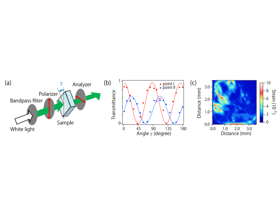
We quantified the strain distribution by taking birefringence images Pinto_Point_2011 . The experimental arrangement is shown in Fig. 1(a). The images of the sample between crossed polarizers were recorded with the rotation angle varied under a microscope. The transmittance at each point can be expressed as
| (1) |
where is the phase difference between the two polarized components of the transmitted light.
The measured -dependence is shown in Fig. 1(b) for two different points on sample 3. The curves of the best fit with Eq. (1), to extract note , are plotted by lines. The change in the refractive index is then obtained as , where is the incident light wavelength and is the sample thickness. Using the refractive index value and the photoelastic constant for diamond Hounsome_Photoelastic_2006 , the magnitude of the strain can be calculated as Pinto_Point_2011 . We used monochromatic light of nm instead of white-light illumination, by inserting a bandpass filter (Thorlabs, FB 560-10). This enabled the elimination of the ambiguity in in determining , and the quantification of a subtle strain (, which is too small to be seen as Raman shift Crisci ) with a spatial resolution of 10 m. The magnitude of the strain at each pixel on sample 2 is shown in color in Fig. 1(c). We found that non-uniform strains were present in each sample.
The maximum value of the strain, , and the strain averaged over the respective sample areas, , were found to increase in the order of samples 1, 2, and 3 (Table I). The strain at the excitation spot, , for TRPL measurements is also listed in Table I, for the centers of samples (spots ) and the off-center of sample 3 (spot 3’).
| Sample/spot | ||||
|---|---|---|---|---|
| (10-5) | 19 | |||
| (10-5) | 4.0 | |||
| (10-5) | 3.7 | |||
Modeling the exciton diffusion - The exciton diffusion was measured using the space-resolved TRPL method reported in Ref. MorimotoPRB . As shown in the inset of Fig. 2, the pulsed laser beam of 2.5 ns duration was focused into a small spot (diameter of m) on the sample to create excitons. The spatial expansion was recorded by imaging the exciton luminescence cloud through a monochromator onto a gated charge-coupled device (CCD) camera (see Supplemental Material). The time evolutions shown in the inset were analyzed as a function of the delay time following photoexcitation. The diffusion coefficient was obtained using the formula derived from the diffusion equation, where is the half width of the exciton cloud. The measurements were repeated at various temperatures and on different samples. The results at four spot positions are plotted in Fig. 2 as a function of the effective temperature of the excitons Hazama . No significant difference was found between the diffusion coefficients at spots 1, 2, and 3’, which indicated that a small amount of strain ( ) did not affect the diffusion coefficient.
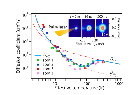
The dashed line in Fig. 2 represents the diffusion coefficient obtained using the calculated rate of acoustic phonon scattering MorimotoPRB , which is in good agreement with the data points up to 80 K. As indicated in Ref. MorimotoPRB , the deviation above 80 K results from the thermal ionization of excitons into electrons and holes with higher mobility. In this paper, we use the ToF mobility reported in the literature ToF and the corresponding diffusion coefficient for electrons (=e) and holes (=h) note1 . As the in-plane electron diffusion is considered an average effect of the propagation of hot electrons (with transverse effective mass , where is the free electron mass) and cool electrons (with longitudinal effective mass ), we use the mean value based on the conductivity effective mass, . Considering that electrons and holes after diffusing around as free carriers then recombine into excitons again, we assume that the product of electron and hole densities propagates with an effective diffusion coefficient of . In Fig. 2, is indicated by a dotted line. The weighted sum of exciton and carrier diffusivity, , is indicated by the thick line, where the exciton fraction is considered according to the law of mass action. In the mass action law, a total carrier density of cm-3, the exciton reduced mass of , and the exciton binding energy of 94 meV were used Ichii . The calculated line is in good agreement with the measured diffusion coefficient in the entire temperature range and it is used in the following analysis.
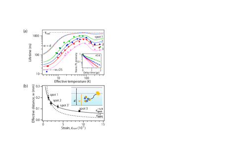
Strain effects on exciton lifetime - A similar series of data as for diffusion enables the extraction of exciton decay times Morimoto_Exciton_2016 . The signal was spatially integrated over the cloud and spectrally integrated over the exciton luminescence for each delay time. The total photoluminescence (PL) intensity was analyzed assuming an exponential decay as shown in the inset of Fig. 3(a). The decay times obtained at spots and 3’ are plotted as a function of temperature in Fig. 3(a). The decay time was shortest at spot 3 where the largest strain was observed. The decay time also exhibited a noticeable temperature dependence.
In previous studies on moderate purity diamonds Takiyama , the decay time was modeled in the range K by considering nonradiative processes in the bulk lifetime, i.e., impurity trapping and exciton ionization. Contrary to this, we found that the impurity trapping occurred significantly slower than the radiative decay in the present samples, based on the upper limits of the impurity concentrations and capture cross sections Shimomura . The possibility of exciton two-body annihilation was also excluded, considering the low exciton density ( cm-3). Therefore, although the bulk lifetime generally includes nonradiative and radiative contributions, the radiative lifetime is crucial in our effectively impurity-free environment. Diamond is an indirect bandgap semiconductor, and thus exhibits slow bulk radiative recombination, with reported radiative lifetimes of 2.3 s Fujii or 750 ns Kozak2013 .
It is known that for various semiconductors, the exciton lifetime can be described by the sum of the rates due to bulk and surface decay, as textbook
| (2) |
Due to the slow bulk decay in diamond, the dominant mechanism limiting the net lifetime is considered as the surface lifetime . The surface lifetime consists of the rate of recombination at the surfaces and the arrival rate of the excitons diffusing to the surfaces. When the sample has two equal sides, the surface lifetime is given by Sproul
| (3) |
where is the surface recombination velocity. The first and second terms are obtained under the limits of and , respectively, for the fundamental-mode solution of the diffusion equation.
By modifying the above formula, we used the relation:
| (4) |
Here, we replaced the sample thickness by an effective distance to a dislocation resulting in the strain, to consider the diffusion to and recombination at the dislocation [see the inset of Fig. 3(b)]. The solid lines in Fig. 3(a) represent calculated by using instead of in Eq. (2). We used as shown in Fig. 2 and adjusted the three parameter values: , , and the bulk lifetime approximated by a radiative lifetime (. We obtained reasonable fitting results with cm/s and s, and here we use the value of s. Our value is slightly smaller than the literature value Kozak2012 . The measured points are nearly perfectly reproduced at , , , and mm for spots and 3’, respectively. The contribution of the surface recombination velocity [the first term in Eq. (4)] is shown for spot 3 by the dash-dotted line, which limits the low-temperature lifetimes only.
A smaller value was obtained at a spot with higher strain. The dependence of on is shown in Fig. 3(b). We empirically found that the data points followed the relationship (solid line) rather than (dashed line). Under the presence of dislocations at density , the arrival time can be expressed as YamaguchiJAP ; SiegAPL . Comparing this with the second term of Eq. (4) results in , 5700, 16000, and 8900 cm-2 for spots and 3’. These values are reasonable considering the state-of-the-art CVD growth with low defect densities Balmer .
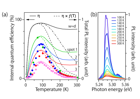
Finally, the dotted lines in Fig. 3(a) represent predictions when is set equal to the sample thickness of mm. For this defect-free case, the exciton decay at intermediate temperatures is limited by the bulk radiative lifetime (; thus, a high internal quantum efficiency of PRAppl ; Kozak_Temperature_2014 ; Fujii can be achieved. The solid lines in Fig. 4(a) indicate calculated using given by Eq. (4). The highest quantum efficiency is expected at 100 K when the diffusion coefficient nearly takes its minimum value. This was observed in the exciton luminescence measured in the time-integrated regime [Fig. 4(b)], and the total PL intensity obtained by spectrally integrating these spectra, as indicated by dots in Fig. 4(a) (see Supplemental Material for details). The drop in the exciton luminescence at high temperature is illustrated by the dashed lines, representing multiplied by the exciton fraction according to the mass action law Ichii . For temperatures below 80 K, the excitons undergo transition to electron-hole droplets whose contribution is difficult to include in the plot due to their very fast nonradiative decay by Auger recombination Shimano .
The plot indicates that excitons are mostly ionized into free carriers at room temperature hBN , which migrate faster than excitons, resulting in a decrease in the lifetime due to the faster diffusion to a dislocation. This decrease can be prevented by increasing the total carrier density and thus increasing and reducing (dash-dotted line). Therefore, to achieve efficient excitonic luminescence from diamond LEDs high-current injection is required. It should be emphasized that the exciton decay is limited by the diffusion-related term for a wide temperature range. Consequently, understanding the exciton diffusion is relevant for determining the exciton lifetime and the luminescence quantum efficiency, which is crucial for the electronic and optoelectronic applications of diamond for efficient devices.
Conclusion - We systematically analyzed the lifetimes of excitons obtained using TRPL measurements in the range of K in extremely high purity CVD diamonds. By excluding the effect of exciton trapping at impurities, we found a clear correlation between the exciton lifetime and the strain magnitude as small as . The temperature dependence of the lifetime was successfully reproduced by the surface recombination model, extended for the case when the strain is acting as a recombination center according to the significant diffusion of excitons. The present study enables the prediction of the temperature-dependent exciton lifetime and luminescence quantum efficiency, which is useful in designing diamond-based devices such as LEDs and radiation detectors. Furthermore, it generally facilitates a better understanding of the optical processes in a wide range of semiconductors with high exciton binding energies.
Acknowledgements.
This work was partially supported by JSPS KAKENHI (Grant Nos. 17H02910, 19K21849, and 15K05129), JSPS bilateral project (No. 120209919), and the Swedish Research Council (Grant No. 2018-04154).References
- (1) I. Aharonovich and E. Neu, Diamond Nanophotonics, Advanced Optical Mater. 2, 911 (2014).
- (2) T. Makino, K. Yoshino, N. Sakai, K. Uchida, S. Koizumi, H. Kato, D. Takeuchi, M. Ogura, K. Oyama, T. Matsumoto, H. Okushi, and S. Yamasaki, Enhancement in emission efficiency of diamond deep-ultraviolet light emitting diode, Appl. Phys. Lett. 99, 061110 (2011).
- (3) F. Staub, H. Hempel, J-Ch. Hebig, J. Mock, U. W. Paetzold, U. Rau, T. Unold, and T. Kirchartz, Beyond Bulk Lifetimes: Insights into Lead Halide Perovskite Films from Time-Resolved Photoluminescence, Phys. Rev. Appl. 6, 044017 (2016).
- (4) K. Takiyama, M. I. Abd-Elrahman, T. Fujita, and T. Oda, Photoluminescence and decay kinetics of indirect free excitons in diamonds under the near-resonant laser excitation, Solid State Commun. 99, 793 (1996).
- (5) R. S. Balmer, J. R. Brandon, S. L. Clewes, H. K. Dhillon, J. M. Dodson, I. Friel, P. N. Inglis, T. D. Madgwick, M. L. Markham, T. P. Mollart, N. Perkins, G. A. Scarsbrook, D. J. Twitchen, A. J. Whitehead, J. J. Wilman, and S. M. Woollard, Chemical vapour deposition synthetic diamond: materials, technology and applications, J. Phys.: Condens. Matter 21, 364221 (2009).
- (6) M. Kozák, F. Trojánek, and P. Malý, Temperature and density dependence of exciton dyanmics in IIa diamond: Experimental and theoretical study, Phys. Status Solidi A 211, 2244 (2014).
- (7) P. Scajev, Excitation and temperature dependent exciton-carrier transport in CVD diamond: Diffusion coefficient, recombination lifetime and diffusion length, Physica B 510, 92 (2017).
- (8) H. Morimoto, Y. Hazama, K. Tanaka, and N. Naka, Ultrahigh exciton diffusion in intrinsic diamond, Phys. Rev. B 92, 201202(R) (2015).
- (9) H. Morimoto, Y. Hazama, K. Tanaka, and N. Naka, Exciton lifetime and diffusion length in high-purity chemical-vapor-deposition diamond, Diam. Relat. Mater. 63, 47 (2016).
- (10) J. Zipfel, M. Kulig, R. Perea-Causin, S. Brem, J. D. Ziegler, R. Rosati, T. Taniguchi, K. Watanabe, M. M. Glazov, E. Malic, and A. Chernikov, Exciton diffusion in monolayer semiconductors with suppressed disorder, Phys. Rev. B 101, 115430 (2020).
- (11) T. Shimomura, Y. Kubo, J. Barjon, N. Tokuda, I. Akimoto, and N. Naka, Quantitative relevance of substitutional impurities to carrier dynamics in diamond Phys. Rev. Mater. 2, 094601 (2018).
- (12) H. Pinto, R. Jones, J. Goss, and P. Briton, Point and extended defects in chemical vapour deposited diamond, J. Phys. Conf. Ser. 281, 012023 (2011).
- (13) The value of was taken as the maximum transmission intensity in the parallel polarizers arrangement at a position where the strain was negligible, to consider the reflection at the sample surfaces. The transmittance never reached unity at any points in the three samples, indicating that the condition was satisfied.
- (14) L. Hounsome, R. Jones, M. Shaw, and P. Briddon, Photoelastic constants in diamond and silicon, Phys. Status Solidi A 203, 3088 (2006).
- (15) A. Cristi, F. Baillet, M. Mermoux, G. Bogdan, M. Nesladek, and K. Haenen, Residual strain around grown-in defects in CVD diamond single crystals: A 2D and 3D Raman imaging study, Phys. Status Solidi A 208, 2038 (2011).
- (16) Y. Hazama, N. Naka, M. Kuwata-Gonokami, and K. Tanaka, Resonant creation of indirect excitons in diamond at the phonon-assisted absorption edge, Euro Phys. Lett. 104, 47012 (2013).
- (17) M. Gabrysch, S. Majdi, D. J. Twitchen and J. Isberg, Electron and hole drift velocity in CVD diamond, J. Appl. Phys. 109, 063719 (2011).
- (18) In Ref. MorimotoPRB , we used the electron mobility obtained using time-resolved cyclotron resonance. However, we recently found that the mobility measured by the time-of-flight method better represents the dc transport property. Details will be published elsewhere.
- (19) T. Ichii, Y. Hazama, N. Naka, and K. Tanaka, Study of detailed balance between excitons and free carriers in diamond using broadband terahertz time-domain spectroscopy, Appl. Phys. Lett. 116, 231102 (2020).
- (20) Dieter K. Schroder, Semiconductor Material and Device Characterization, 3rd ed. (John Wiley & Sons, 2015) ISBN0471739065.
- (21) A. Fujii, K. Takiyama, R. Maki, and T. Fujita, Lifetime and quantum efficiency of luminescence due to indirect excitons in a diamond, J. Lumin. 94-95, 355 (2001).
- (22) M. Kozák, F. Trojánek, and P. Malý, Optical study of carrier diffusion and recombination in CVD diamond, Phys. Status Solidi A 210, 2008 (2013).
- (23) A. B. Sproul, Dimensionless solution of the equation describing the effect of surface recombination on carrier decay in semiconductors, J. Appl. Phys. 76, 2851 (1994).
- (24) M. Kozák, F. Trojánek, and P. Malý, Large prolongation of free-exciton photoluminescence decay in diamond by two-photon excitation, Opt. Lett. 37, 2049 (2012).
- (25) M. Yamaguchi and C. Amano, Efficiency calculation of thin-film GaAs solar cells on Si substrates, J. Appl. Phys. 58, 3601 (1985).
- (26) R. M. Sieg, J. A. Carlin, J. J. Boeckl, and S. A. Ringel, High minority-carrier lifetimes in GaAs grown on low-defect-density Ge/GeSi/Si substrates, Appl. Phys. Lett. 73, 3111 (1998).
- (27) R. Shimano, M. Nagai, K. Horiuchi, and M. Kuwata-Gonokami, Formation of a High Tc Electron-Hole Liquid in Diamond, Phys. Rev. Lett. 88, 057404 (2002).
- (28) L. Schue, L. Sponza, A. Plaud, H. Bensalah, K. Watanabe, T. Taniguchi, F. Ducastelle, A. Loiseau, and J. Barjon, Bright Luminescence from Indirect and Strongly Bound Excitons in h-BN, Phys. Rev. Lett. 122, 067401 (2019).
Supplementary Material
Diffusion-related lifetime of indirect excitons in diamond
K. Konish,1 I. Akimoto,2 J. Isberg,3 Nobuko Naka1
1Department of Physics, Kyoto University, Kitashirakawa-Oiwake-cho, Sakyo-ku, Kyoto 606-8502, Japan
2Department of Materials Science and Chemistry, Wakayama University, Wakayama 640-8510, Japan
3Department of Electrical Engineering, Uppsala University, Box 65, S-751 03 Uppsala, Sweden
S1 Measurement of diffusion coefficient
The method for extracting the diffusion coefficient of excitons in diamond was reported in our previous paper [1]; here, we summarize the main points only.
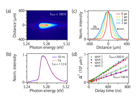
The sample was mounted in a closed-cycle cryostat and the temperature was measured by a silicon diode thermometer attached to the sample holder. The excitation light source was an output from an optical parametric oscillator pumped by a YAG laser (Ekspla, NT242-2). The excitation wavelength was 225 nm and the penetration length was approximately 500 m at 100 K (see also Sect. S2), comparable to the sample thickness. The luminescence from the sample was imaged onto the entrance slit of the monochromator (Horiba Jobin Yvon, iHR550) by a pair of achromatic lenses with a magnification factor of . Two exit ports were implemented in the monochromator; one was used for detection by a gated-ICCD camera (LaVision, PicoStarHR) synchronized to the trigger from the laser, the other for detection by a CCD camera (Andor, Newton DU940N) in a time-integrated regime. To ensure to collect the exciton luminescence only, the grating was set at the first-order diffraction mode and the luminescence was spectrally resolved with the spatial information retained along the vertical slit of the monochromator. Figure S1(a) shows the spectral image at a 50 ns delay time obtained with sample 1 at 100 K.
Figure S1(b) shows the luminescence spectrum obtained by vertically integrating the counts shown in Fig. S1(a). The major peak is due to the recombination of the indirect exciton accompanied by the emission of a transverse-optical (TO) phonon. Intuitively, the width at temperature is 1.8 , where is the Boltzmann constant. More precisely, the effective temperature of excitons can be obtained by spectral fitting using the Maxwell-Boltzmann distribution: , where is a normalization factor and is the photon energy measured from the edge [2]. We included four fine-structure exciton levels and the effect of spectral broadening due to the finite width of the entrance slit by convolution. The best fit function is indicated by the dashed line. The effective temperature K was slightly higher than K, and the temperature increase was slightly different depending on samples.
Figure S1(c) shows the spatial profiles at different delay times, obtained by spectrally integrating the luminescence image over the TO phonon assisted line. The profile was then fitted by a Gaussian function to extract the half width, . Figure S1(d) shows the squared half width as a function of the delay time . A linear time dependence is expected from the diffusion equation, and the lines are fits to obtain the diffusion coefficient, .
Similar measurements and analyses were performed for four different spot positions and at various temperatures, providing the data points shown in Fig. 2 of the main text.
S2 Measurement of luminescence intensity
The exciton luminescence intensity measurements are fundamentally simple. In the following, we describe the effect of electron-hole droplets (EHDs) and certain corrections performed for the accurate evaluation of the intensity.
Figure S2(a) shows the time-integrated photoluminescence (PL) spectra obtained from spot 3’ for temperature varied from 300 K to 7 K. The spectral range is wider than that shown in Fig. S1(b), and the transverse-acoustic (TA) and two-phonon assisted lines can be seen in addition to the TO phonon assisted line at 5.27 eV. Both the spectral width and intensity changed drastically with the temperature. The broadening of the line with increasing temperature was consistent with the thermal distribution of 1.8 , as explained above.
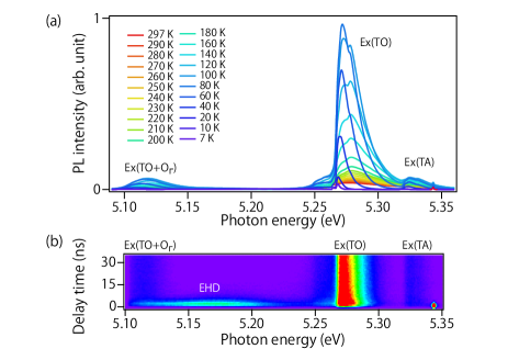
As mentioned in the main text, there were a few missing counts below 80 K due to the EHD formation. Figure S2(b) shows the time-resolved luminescence spectrum following photoexcitation. The broad structure seen in the range of eV is due to the recombination of the EHD. The decay is very fast ns), and its contribution can hardly be seen in the spectra obtained in the time-integrated regime [Fig. S2(a)]. For a typical incident laser power of W used in our experiments, the EHD signal was observed below 80 K in the time-resolved regime.
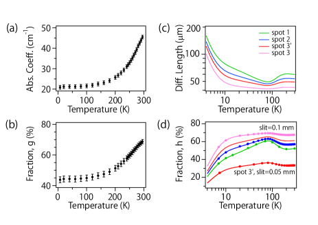
For the exciton luminescence efficiency, we spectrally integrated the time-integrated signal counts from 5.05 to 5.40 eV covering the three phonon-assisted lines. Then, we corrected the counts by the laser power absorbed by the sample. The laser wavelength was fixed at 225 nm for the whole temperature range, but the absorption coefficient is known to be temperature dependent. As shown in Fig. S3(a), the absorption coefficient increases exponentially with the temperature according to the increase in the phonon occupation number. The fraction of the absorbed photon over the total photon numbers was estimated using the Beer-Lambert law for the measured absorption coefficient and the sample thickness . The calculated fraction is plotted in Fig. S3(b), varying from 70 % at room temperature to 45 % at 10 K, where the reflectivity at the sample surface () is assumed to be independent of the temperature. This effect has been corrected for the data points in Fig. 4(a) in the main text.
Furthermore, the luminescence signals are partially lost when the entrance slit of the monochromator is narrow. We considered this effect by calculating the fraction of the luminescence photons entering the monochromator using , where is the width of the monochromator slit and is the magnification factor. We assumed a temperature-dependent Gaussian broadening with the diffusion length , whose temperature dependence is plotted in Fig. S3(c). As can be seen in Fig. S3(d), the effect of is not significant above 10 K and when the slit is open at 0.1 mm.
To summarize, the total PL intensity shown in Fig. 4(a) is the spectrally integrated intensity corrected by the factors and . It should be noted that these counts are not absolute photon numbers, as we did not consider the efficiencies resulting from the solid angle of detection and conversion from photon to electron counts in the CCD camera. Thus, the counts are shown in a relative unit on the right axis of Fig. 4(a).
REFERENCES
[1] H. Morimoto, Y. Hazama, K. Tanaka, and N. Naka,
Phys. Rev. B 92, 201202(R) (2015).
[2] Y. Hazama, N. Naka, M. Kuwata-Gonokami, and K.
Tanaka, Euro Phys. Lett. 104, 47012 (2013).