]Authors to whom correspondence should be addressed: cwfink@berkeley.edu, samwatkins@berkeley.edu ]Authors to whom correspondence should be addressed: cwfink@berkeley.edu, samwatkins@berkeley.edu Now at ]Department of Physics, Virginia Tech, Blacksburg, VA 24061, USA Now at ]Department of Applied Physics and Yale Quantum Institute, Yale University, New Haven, CT 06511, USA CPD Collaboration
Performance of a Large Area Photon Detector for Rare Event Search Applications
Abstract
We present the design and characterization of a large-area Cryogenic PhotoDetector (CPD) designed for active particle identification in rare event searches, such as neutrinoless double beta decay and dark matter experiments. The detector consists of a surface area by 1-mm-thick Si wafer. It is instrumented with a distributed network of Quasiparticle-trap-assisted Electrothermal feedback Transition-edge sensors (QETs) with superconducting critical temperature to measure athermal phonons released from interactions with photons. The detector is characterized and calibrated with a collimated 55Fe X-ray source incident on the center of the detector. The noise equivalent power is measured to be in a bandwidth of . The baseline energy resolution is measured to be (RMS). The detector also has an expected timing resolution of for events.
In rare event searches, experimental sensitivity is often limited by background signals Alduino et al. (2018); Adams et al. (2020); Andreotti et al. (2011); Armengaud et al. (2019); Angloher et al. (2017); Arnaud et al. (2020); Agnese et al. (2018); Abramoff et al. (2019); Aguilar-Arevalo et al. (2019); Abdelhameed et al. (2019). Developing precision detectors to veto background and noise signals has been a high priority in these fields. Much interest in low temperature cryogenic detector technology has been shown by groups carrying out searches for neutrinoless double beta decay Avignone III, Elliott, and Engel (2008) (), such as the CUORE Alduino et al. (2018); Adams et al. (2020), CUPID Armstrong et al. (2019), and AMoRE Alenkov et al. (2019) experiments. In these low-temperature calorimeters, the dominant source of background events consists of decays from the surrounding environment Alduino et al. (2018); Adams et al. (2020); Azzolini:2019nmi. It has been shown that Cherenkov emission or scintillation light can be used to positively identify the signal s, allowing for background discrimination Tabarelli de Fatis (2010). In order for these experiments to achieve a high level of rejection for these backgrounds, photon detectors with large surface areas and baseline energy resolutions below (RMS) for Cherenkov signals Casali et al. (2015), or of for scintillation signals Armstrong et al. (2019), are required. To reject the pileup background from multiple ordinary (two neutrino) double beta decay () events, experiments need timing resolutions down to (for the 100Mo isotope) Armstrong et al. (2019).
There has also been theoretical and experimental motivation to search for dark matter (DM) in the mass range of to Battaglieri et al. (2017); Essig, Mardon, and Volansky (2012); Essig et al. (2013); Alexander et al. (2016). However, current experiments have been limited by unknown background signals in the energy range of (1-100) Armengaud et al. (2019); Angloher et al. (2017); Arnaud et al. (2020); Agnese et al. (2018); Abramoff et al. (2019); Aguilar-Arevalo et al. (2019); Abdelhameed et al. (2019); Kurinsky et al. (2020). If the source of such backgrounds are high energy photons that deposit only an extremely small fraction of their energy in the target Robinson (2017), then a nearly active shield composed of high- scintillating crystals read out by these large area photon detectors could be highly efficient at suppressing these backgrounds. Additionally, a sensitive large area cryogenic detector could be useful for discriminating small energy depositions due to radiogenic surface backgrounds. Other potential DM applications for this detector technology include searches for inelastic electronic recoils off scintillating crystals and searches for interactions with superfluid He Derenzo et al. (2017); Knapen et al. (2018); Hertel et al. (2019).
We present the characterization of a large area Cryogenic PhotoDetector (CPD) with a measured baseline energy resolution of (RMS) and a timing resolution of for events that meets or exceeds the technical requirements for the currently proposed experiments and DM searches. This is the first demonstration of the capabilities of such detectors, and further development may open opportunities for more novel applications.
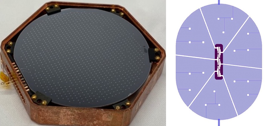
The (100)-oriented substrate of the CPD is a Si wafer of thickness and a surface area of . A parallel network of 1031 Quasiparticle-trap-assisted Electrothermal feedback Transition-edge sensors (QETs) Irwin and Hilton (2005); Irwin et al. (1995) with was deposited on one side of the wafer. The QETs are uniformly distributed over the wafer’s surface and connected to a single readout channel. The uniform and distributed nature of the channel allows for the fast collection of athermal phonons with minimal positional dependence, reducing efficiency penalties from effects such as athermal phonon down-conversion Knaak et al. (1986); Kozorezov et al. (2000). The opposite side of the Si wafer is unpolished and noninstrumented. The detector and QET mask design can be seen in Fig. 1. In Table 1, the QET design specifications for the CPD are listed.
| Specification | Value |
| TES Length | 140 |
| TES Thickness | 40 |
| TES Width | 3.5 |
| Number of Al Fins | 6 |
| Al Fin Length | 200 |
| Al Fin Thickness | 600 |
| Al-W Overlap | 10 |
| Number of QETs | 1031 |
| Active Surface Area | 1.9 |
| Passive Surface Area | 0.2 |
The detector was studied at the SLAC National Accelerator Laboratory in a cryogen-free dilution refrigerator at a bath temperature () of . The detector was placed in a copper housing and was held mechanically with the use of six cirlex clamps. The cirlex clamps also provided the thermal link between the detector and the copper housing. The QET arrays were voltage biased and the current through the TES was measured with a DC superconducting quantum interference device (SQUID) array with a measured noise floor of .
A collimated X-ray source was placed inside the cryostat and was incident upon the noninstrumented side of the CPD in the center of the detector. A layer of Al foil was placed inside the collimator to provide a calibration line from fluorescence at Schweppe et al. (1994); Hölzer et al. (1997). The collimator was tuned such that there was of the Kα and Kβ decays incident on the detector. The detector was held at a bath temperature for approximately two weeks to allow any parasitic heat added by the cirlex clamps to dissipate. During this time, we attempted to neutralize potential charged impurities within the Si wafer as much as possible with ionization produced by a source placed outside of the cryostat.
To characterize the QETs, sweeps were taken at various bath temperatures by measuring TES quiescent current as a function of bias current111Although we are applying a bias current, we use the term “” because the voltage and current are related by the shunt resistor: , with superimposed small square pulses providing complex admittance Irwin and Hilton (2005) at each point in the curve Fink et al. (2020); Pyle (2012); Kurinsky (2018). Since all the QETs are connected in parallel in a single channel, the channel was treated as if it were a single QET, describing the average characteristics of the total array. The data allowed for the estimation of the parasitic resistance in the TES line (), the normal state resistance (), and the nominal bias power (). The effective thermal conductance between the QETs to the Si wafer () and were measured by fitting a power law to the measured bias power as a function of bath temperature Fink et al. (2020). This measurement is a lower bound of these values, as it assumes no parasitic bias power in the system. We summarize these characteristics of the detector in Table 2.
| Parameter | Value |
|---|---|
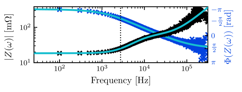
The complex admittance data allows us to estimate the dynamic properties of the sensors. Throughout the superconducting transition, primary and secondary thermal fall times were observed, e.g. and , respectively, at . The origin of this additional time constant is under investigation. Its appearance suggests that we have a more complex thermal or electrical system, e.g. phase separation Cabrera (2008); Pyle (2012) or an extra heat capacity connected to the TES heat capacity Maasilta (2012). A characteristic plot of complex impedance of the TES circuit can be seen in Fig. 2.
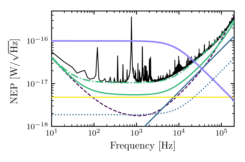
Knowledge of the TES parameters, given in Table 2, allowed for the calculation of the power-to-current responsivity, which was used to convert the measured current-referred power spectral density (PSD) to the noise equivalent power (NEP). These parameters were used to predict the expected noise spectrum using the single-heat-capacity thermal model Irwin and Hilton (2005). A comparison of the NEP to the model at can be seen in Fig 3. The excess noise spikes above approximately have been experimentally confirmed to be largely caused by vibrations from the operation of the pulse tube cryocooler. The observed noise is also elevated above our model at frequencies in the effective sensor bandwidth interval (approximately the inverse of the thermal time constant Irwin and Hilton (2005)) by a factor of , as compared to the prediction. This “in-band” excess noise is consistent with two different hypotheses: a white power noise spectrum incident on the detector of (e.g. a light leak) or a parasitic DC power in the bias circuit of approximately . If we assume the latter is the source, this allows us to calculate the upper bounds on our estimates of and , as reported in Table 2. There remains bias-dependent excess noise above the sensor bandwidth. We parameterize the excess TES Johnson–like noise with the commonly used factor Irwin and Hilton (2005); Jethava et al. (2009). Using values of up to 1.8, depending on bias point, can account for the discrepancy between observation and prediction at these frequencies. We note that this “excess” noise could possibly also be explained with a more complex thermal model.
The lowest integrated NEP was achieved at an optimum bias point of . In addition to the characterization data, approximately 500,000 threshold triggered events and 80,000 randomly triggered events were recorded at this bias.
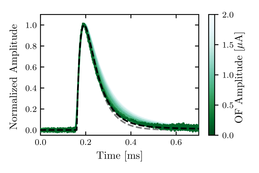
For the measured phonon-pulse shape, there are multiple characteristic time constants. The pulse rise time was measured as , which is the expected characteristic time scale for athermal phonons being absorbed by the Al collection fins of the QETs for this design. The dominant pulse fall time is consistent with the expectation from the complex impedance as we approach zero-energy, where we confirmed the expected thermal time constant via a fit of the rise and fall times of the pulses. The secondary time constant from the complex impedance of was also seen in these low-energy pulses. The secondary time constant from the complex impedance of was also seen in these low-energy pulses, with an amplitude ratio of less than to the dominant decay exponential.
We observed an additional long-lived behavior in the pulses, which can be estimated as a low-amplitude exponential tail whose magnitude scales linearly with the event energy. As this tail is not seen in the complex impedance data, it might be due to direct absorption of phonons with energy smaller than the Al superconducting band gap into the TES Irwin et al. (1995).
For energies above , we observed a local saturation effect that manifests as the dominant fall time lengthening with increased energy. In Fig. 4, we show averaged pulses for various event amplitudes, showing the dependence of the pulse fall time on energy. We associate this effect with high-energy, single-particle events pushing nearby QETs into the normal resistance regime, slowing down the response of the total single-channel device. We also note that there is a position-dependent effect for a subset of high-energy events, notable by a varying fall time for events with the same amplitude. Our hypothesis for this phenomenon is that events close to the edge of the detector have less solid angle to deposit the energy, which leads to longer recovery times as opposed to events in the center of the detector (e.g. the calibration events). These effects are specific to the single-particle nature of the measured events. For scintillation events, the isotropic nature of the photons would spread out the event energy across the entire detector channel, avoiding these local saturation and position-dependent effects.
To reconstruct event energies, two energy estimators were used in this analysis: the optimum filter (OF) amplitude Zadeh and Ragazzini (1952); Golwala (2000) and the energy removed by electrothermal feedback () Irwin and Hilton (2005). For the OF, we used an offline algorithm to reconstruct energies. A single noise spectrum was used, which was computed from the randomly triggered events. The phonon-pulse template used was an analytic template that matches the measured low-energy pulse shape, neglecting the low-amplitude tail. Because we could not directly measure the low-energy phonon-pulse shape with high statistics, we used a template without the long-lived behavior.
The integral estimator was calculated for each triggered event by measuring the decrease in Joule heating via
| (1) |
where is the time at which the integral is truncated, is the baseline-subtracted pulse in current, is the quiescent current through the TES, is the load resistance, and is the voltage bias of the TES circuit Irwin and Hilton (2005). In comparison to the OF amplitude, this integral estimator was less sensitive to saturation effects, but had a worse baseline energy resolution. When characterizing this device, we used the integral truncation of for . This was done to preserve good baseline energy sensitivity in this integral estimator when calibrating the OF amplitude energy estimator at low energies.
For pulse-shape saturation at high energies, we use the following empirical model:
| (2) |
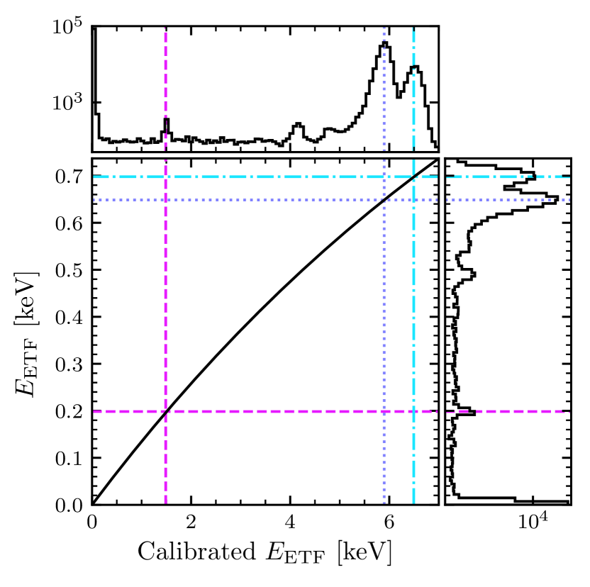
This functional form has the expected behavior: it intercepts zero, approaches an asymptotic value at high energies, and becomes linear for small values of . In Fig. 5, the fitted saturation model, as well as the calibrated and uncalibrated spectra, are shown, as compared to the energies of various spectral peaks in both energy scales. For the event spectra, we observed an unknown background at low energies. As other surface experiments have seen excess backgrounds at similar energies Armengaud et al. (2019); Angloher et al. (2017), we do not expect this to be detector-dependent. We are actively studying this detector at an underground facility, for which the results will be published in a future work.
The absolute phonon collection efficiency () of the detector was estimated by measuring at the lowest energy calibration line (Al fluorescence) and dividing by the known energy of that line. Because of the long-lived behavior in the phonon-pulse shapes, the measured collection efficiency of this detector depends on the integration truncation time . If it is chosen to only include energy collected by the first sensor fall time (e.g. ), then we find that . Alternatively, if we integrate to effectively infinity, this includes the low-amplitude long-lived behavior of the phonon pulses. In this case, the collection efficiency increases to , which implies that about of the collected energy for a given event is associated with the low-amplitude tail of the phonon-pulse shape (about 8% and 22% from the and components, respectively).
To calibrate the OF amplitude to units of energy, we fit the relationship between the calibrated and the OF amplitude to a linear slope at low energies (below approximately ). This method does not provide a calibration of the OF amplitude at high energies, but allows for the calculation of the baseline energy resolution.
For the calibration method used, the main source of systematic error is the saturation model in Eq. (2). Since it is empirical, its use introduces uncertainty in its applicability. We can estimate the upper bound of the effect of this systematic on the baseline energy resolution as the value that would be reached if we instead calibrated linearly using the Al fluorescence line. In this case, this worsens the baseline energy resolution, as we are not taking into account the expected response (see Fig. 5).
The baseline energy resolution was calculated as the RMS of 46,000 randomly triggered events, after removing data contaminated by pileup events, electronic glitches, or thermal tails. This gave a resolution of (RMS) for the OF energy estimator, where these data are consistent with a normal distribution. This is in agreement with our estimation from the observed NEP and the power-referred phonon-pulse shape (a single-exponential with fall time and collection efficiency ), which gave an expected baseline energy resolution of (RMS), as was similarly done in Ref. Fink et al., 2020.
Using the OF formalism, we can also calculate the expected timing resolution Golwala (2000) of the CPD, which provides an estimate of the minimum resolving time for two pileup events. For a event, the corresponding timing resolution of this detector is . For many experiments, the minimum resolving time requirement to make pileup of multiple events a negligible background is on the order of Chernyak et al. (2012); Artusa et al. (2014); Pyle, Figueroa-Feliciano, and Sadoulet (2015); Casali et al. (2019). For the CUPID and CUPID-1T experiments, this requirement is about and , respectively Armstrong et al. (2019). An initial study of pileup events was carried out by adding two simulated pulses of randomized time separation to the in-run randomly triggered events from the CPD dataset. In this simulation, we observed that minimum resolving times below are achievable with an OF-based pileup detection algorithm. In the future, we will study the minimum resolving time with a more detailed simulation based on the expected spectrum for 100Mo. Given these initial studies, we expect the CPD to fulfill these requirements.
When comparing the baseline energy resolution of the CPD to the requirements of the CUPID experiment, the value surpasses the requirement of less than (RMS) by a factor of five. While the CPD is a TES-based detector, it has been shown that Microwave Kinetic Inductance Detectors (MKIDs) and Neutron-Transmutation-Doped (NTD) Ge detectors are also promising avenues for achieving the sub- baseline goal. In Table 3, we report this result alongside those of other detectors for this application. In comparison to the devices that have met or exceeded the requirement, the CPD does not require Neganov-Trofimov-Luke (NTL) amplification Neganov and Trofimov (1985); Luke (1988) (which often results in excess dark counts) and has the best baseline energy sensitivity for its size.
| Device | Area | NTL? | ||
|---|---|---|---|---|
| MKID Cardani et al. (2018) | 4.0 | 26 | 13 | No |
| W-TES Schäffner et al. (2015) | 12.6 | 23 | 6.5 | No |
| Ge-NTD Barucci et al. (2019) | 15.6 | 20 | 5.1 | No |
| Ge-NTD Pattavina et al. (2015) | 19.6 | 19 | 4.3 | Yes |
| IrAu-TES Willers et al. (2015) | 4.0 | 7.8 | 3.9 | Yes |
| Ge-NTD Armengaud et al. (2017) | 4.9 | 7.6 | 3.5 | Yes |
| Ge-NTD Bergé et al. (2018) | 15.2 | 10 | 2.6 | Yes |
| Ge-NTD Novati et al. (2019) | 15.2 | 8 | 2.1 | Yes |
| W-TES Rothe et al. (2018) | 12.6 | 4.1 | 1.2 | No |
| W-TES (this) | 45.6 | 3.9 | 0.6 | No |
The measured baseline energy resolution of and the expected timing resolution of (at ), combined with its large surface area, makes this detector an excellent candidate for background rejection in both and DM experiments. Because of the energy sensitivity, this device can be used as a dark matter detector itself, as we have done in collaboration with SuperCDMS to set limits on spin-independent dark matter-nucleon interactions for sub- dark matter particle masses Alkhatib et al. (2020). Similarly, this gram-scale device could be applied to coherent elastic neutrino-nucleus scattering experiments Papoulias, Kosmas, and Kuno (2019). The performance of the CPD can be further optimized through adjustment of characteristics such as the Al-W overlap and overall Al coverage. From these considerations, we anticipate up to a factor of two improvement in baseline energy resolution for a future iteration of the CPD, which is currently being designed.
Authors C.W.F. and S.L.W. contributed equally to this work. This material is based upon work supported by the US Department of Energy (DOE) Office of Science under Contract Nos. DE-AC02-05CH11231 and DE-AC02-76SF00515, by the DOE Office of Science, Office of High Energy Physics under Contract Nos. KA-2401032, DE-SC0018981, and DE-SC0017859, by the National Science Foundation (NSF) under Grant Nos. PHY-1314881, PHY-1415388, and PHY-1809769, and by Michael M. Garland.
The data that support the findings of this study are available upon reasonable request to the corresponding authors.
References
- Alduino et al. (2018) C. Alduino et al. (CUORE Collaboration), Phys. Rev. Lett. 120, 132501 (2018).
- Adams et al. (2020) D. Q. Adams et al. (CUORE Collaboration), Phys. Rev. Lett. 124, 122501 (2020).
- Andreotti et al. (2011) E. Andreotti et al., Astropart. Phys. 34, 822 (2011).
- Armengaud et al. (2019) E. Armengaud et al. (EDELWEISS Collaboration), Phys. Rev. D 99, 082003 (2019).
- Angloher et al. (2017) G. Angloher et al. (CRESST Collaboration), Eur. Phys. J. C 77, 637 (2017).
- Arnaud et al. (2020) Q. Arnaud et al. (EDELWEISS Collaboration), Phys. Rev. Lett. 125, 141301 (2020).
- Agnese et al. (2018) R. Agnese et al. (SuperCDMS Collaboration), Phys. Rev. Lett. 121, 051301 (2018).
- Abramoff et al. (2019) O. Abramoff et al. (SENSEI Collaboration), Phys. Rev. Lett. 122, 161801 (2019).
- Aguilar-Arevalo et al. (2019) A. Aguilar-Arevalo et al. (DAMIC Collaboration), Phys. Rev. Lett. 123, 181802 (2019).
- Abdelhameed et al. (2019) A. H. Abdelhameed et al. (CRESST Collaboration), Phys. Rev. D 100, 102002 (2019).
- Avignone III, Elliott, and Engel (2008) F. T. Avignone III, S. R. Elliott, and J. Engel, Rev. Mod. Phys. 80, 481 (2008).
- Armstrong et al. (2019) W. R. Armstrong et al. (CUPID Collaboration), arXiv:1907.09376 (2019).
- Alenkov et al. (2019) V. Alenkov et al., Eur. Phys. J. C 79, 791 (2019).
- Tabarelli de Fatis (2010) T. Tabarelli de Fatis, Eur. Phys. J. C 65, 359 (2010).
- Casali et al. (2015) N. Casali, M. Vignati, J. W. Beeman, F. Bellini, L. Cardani, I. Dafinei, S. Di Domizio, F. Ferroni, L. Gironi, S. Nagorny, et al., Eur. Phys. J. C 75, 12 (2015).
- Battaglieri et al. (2017) M. Battaglieri et al., arXiv:1707.04591 (2017).
- Essig, Mardon, and Volansky (2012) R. Essig, J. Mardon, and T. Volansky, Phys. Rev. D 85, 076007 (2012).
- Essig et al. (2013) R. Essig et al., arXiv:1311.0029 (2013).
- Alexander et al. (2016) J. Alexander et al., arXiv:1608.08632 (2016).
- Kurinsky et al. (2020) N. Kurinsky, D. Baxter, Y. Kahn, and G. Krnjaic, Phys. Rev. D 102, 015017 (2020).
- Robinson (2017) A. E. Robinson, Phys. Rev. D 95, 021301 (2017).
- Derenzo et al. (2017) S. Derenzo, R. Essig, A. Massari, A. Soto, and T.-T. Yu, Phys. Rev. D 96, 016026 (2017).
- Knapen et al. (2018) S. Knapen, T. Lin, M. Pyle, and K. M. Zurek, Phys. Lett. B 785, 386 (2018).
- Hertel et al. (2019) S. A. Hertel, A. Biekert, J. Lin, V. Velan, and D. N. McKinsey, Phys. Rev. D 100, 092007 (2019).
- Irwin and Hilton (2005) K. D. Irwin and G. C. Hilton, “Transition-edge sensors,” in Cryogenic Particle Detection, edited by C. Enss (Springer Berlin Heidelberg, Berlin, Heidelberg, 2005) pp. 63–150.
- Irwin et al. (1995) K. D. Irwin, S. W. Nam, B. Cabrera, B. Chugg, and B. A. Young, Rev. Sci. Instrum. 66, 5322 (1995).
- Knaak et al. (1986) W. Knaak, T. Hauß, M. Kummrow, and M. Meißner, in Phonon Scattering in Condensed Matter V, edited by A. C. Anderson and J. P. Wolfe (Springer Berlin Heidelberg, Berlin, Heidelberg, 1986) pp. 174–176.
- Kozorezov et al. (2000) A. G. Kozorezov, A. F. Volkov, J. K. Wigmore, A. Peacock, A. Poelaert, and R. den Hartog, Phys. Rev. B 61, 11807 (2000).
- Schweppe et al. (1994) J. Schweppe, R. D. Deslattes, T. Mooney, and C. J. Powell, J. Electron Spectrosc. 67, 463 (1994).
- Hölzer et al. (1997) G. Hölzer, M. Fritsch, M. Deutsch, J. Härtwig, and E. Förster, Phys. Rev. A 56, 4554 (1997).
- Note (1) Although we are applying a bias current, we use the term “” because the voltage and current are related by the shunt resistor: .
- Fink et al. (2020) C. W. Fink, S. L. Watkins, T. Aramaki, P. L. Brink, S. Ganjam, B. A. Hines, M. E. Huber, N. A. Kurinsky, R. Mahapatra, N. Mirabolfathi, et al., AIP Adv. 10, 085221 (2020).
- Pyle (2012) M. Pyle, Optimizing the design and analysis of cryogenic semiconductor dark matter detectors for maximum sensitivity, Ph.D. thesis, Stanford University (2012).
- Kurinsky (2018) N. Kurinsky, The Low-Mass Limit: Dark Matter Detectors with eV-Scale Energy Resolution, Ph.D. thesis, Stanford University (2018).
- Cabrera (2008) B. Cabrera, J. Low Temp. Phys. 151, 82 (2008).
- Maasilta (2012) I. J. Maasilta, AIP Adv. 2, 042110 (2012).
- Jethava et al. (2009) N. Jethava, J. N. Ullom, K. D. Irwin, W. B. Doriese, J. A. Beall, G. C. Hilton, L. R. Vale, and B. Zink, AIP Conf. Proc. 1185, 31 (2009).
- Zadeh and Ragazzini (1952) L. A. Zadeh and J. R. Ragazzini, Proc. IRE 40, 1223 (1952).
- Golwala (2000) S. R. Golwala, Exclusion limits on the WIMP nucleon elastic scattering cross-section from the Cryogenic Dark Matter Search, Ph.D. thesis, University of California, Berkeley (2000).
- Reed and Ware (1972) S. J. B. Reed and N. G. Ware, J. Phys. E Sci. Instrum. 5, 582 (1972).
- Chernyak et al. (2012) D. M. Chernyak, F. A. Danevich, A. Giuliani, E. Olivieri, M. Tenconi, and V. I. Tretyak, Eur. Phys. J. C 72, 1989 (2012).
- Artusa et al. (2014) D. R. Artusa et al., Eur. Phys. J. C 74, 3096 (2014).
- Pyle, Figueroa-Feliciano, and Sadoulet (2015) M. Pyle, E. Figueroa-Feliciano, and B. Sadoulet, arXiv:1503.01200 (2015).
- Casali et al. (2019) N. Casali, L. Cardani, I. Colantoni, A. Cruciani, S. Di Domizio, M. Martinez, G. Pettinari, and M. Vignati, Eur. Phys. J. C 79, 724 (2019).
- Neganov and Trofimov (1985) B. S. Neganov and V. N. Trofimov, Otkryt. Izobret. 146, 215 (1985).
- Luke (1988) P. N. Luke, J. Appl. Phys. 64, 6858 (1988).
- Cardani et al. (2018) L. Cardani, N. Casali, A. Cruciani, H. le Sueur, M. Martinez, F. Bellini, M. Calvo, M. G. Castellano, I. Colantoni, C. Cosmelli, et al., Supercond. Sci. Technol. 31, 075002 (2018).
- Schäffner et al. (2015) K. Schäffner, G. Angloher, F. Bellini, N. Casali, F. Ferroni, D. Hauff, S. S. Nagorny, L. Pattavina, F. Petricca, S. Pirro, et al., Astropart. Phys. 69, 30 (2015).
- Barucci et al. (2019) M. Barucci, J. W. Beeman, V. Caracciolo, L. Pagnanini, L. Pattavina, G. Pessina, S. Pirro, C. Rusconi, and K. Schäffner, Nucl. Instrum. Methods Phys. Res. A 935, 150 (2019).
- Pattavina et al. (2015) L. Pattavina, N. Casali, L. Dumoulin, A. Giuliani, M. Mancuso, P. de Marcillac, S. Marnieros, S. S. Nagorny, C. Nones, E. Olivieri, et al., J. Low Temp. Phys. 184, 286–291 (2015).
- Willers et al. (2015) M. Willers, F. v. Feilitzsch, A. Gütlein, A. Münster, J.-C. Lanfranchi, L. Oberauer, W. Potzel, S. Roth, S. Schönert, M. v. Sivers, et al., J. Instrum. 10, P03003 (2015).
- Armengaud et al. (2017) E. Armengaud et al., Eur. Phys. J. C 77, 785 (2017).
- Bergé et al. (2018) L. Bergé et al., Phys. Rev. C 97, 032501 (2018).
- Novati et al. (2019) V. Novati, L. Bergé, L. Dumoulin, A. Giuliani, M. Mancuso, P. de Marcillac, S. Marnieros, E. Olivieri, D. V. Poda, M. Tenconi, et al., Nucl. Instrum. Methods Phys. Res. A 940, 320–327 (2019).
- Rothe et al. (2018) J. Rothe, G. Angloher, P. Bauer, A. Bento, C. Bucci, L. Canonica, A. D’Addabbo, X. Defay, A. Erb, F. v. Feilitzsch, et al., J. Low Temp. Phys. 193, 1160 (2018).
- Alkhatib et al. (2020) I. Alkhatib et al. (SuperCDMS Collaboration), arXiv:2007.14289 (2020).
- Papoulias, Kosmas, and Kuno (2019) D. K. Papoulias, T. S. Kosmas, and Y. Kuno, Front. Phys. 7, 191 (2019).