CMOS-based cryogenic control of silicon quantum circuits
The most promising quantum algorithms require quantum processors hosting millions of quantum bits when targeting practical applications Van Meter and Horsman (2013). A major challenge towards large-scale quantum computation is the interconnect complexity. In current solid-state qubit implementations, a major bottleneck appears between the quantum chip in a dilution refrigerator and the room temperature electronics. Advanced lithography supports the fabrication of both CMOS control electronics and qubits in silicon. When the electronics are designed to operate at cryogenic temperatures, it can ultimately be integrated with the qubits on the same die or package, overcoming the wiring bottleneck Vandersypen et al. (2017); Patra et al. (2018); Pauka et al. (2019); Geck et al. (2019). Here we report a cryogenic CMOS control chip operating at 3 K, which outputs tailored microwave bursts to drive silicon quantum bits cooled to 20 mK. We first benchmark the control chip and find electrical performance consistent with 99.99% fidelity qubit operations, assuming ideal qubits. Next, we use it to coherently control actual silicon spin qubits Watson et al. (2018); Zajac et al. (2017); Huang et al. (2019) and find that the cryogenic control chip achieves the same fidelity as commercial instruments. Furthermore, we highlight the extensive capabilities of the control chip by programming a number of benchmarking protocols as well as the Deutsch-Josza algorithm Deutsch and Jozsa (1992) on a two-qubit quantum processor. These results open up the path towards a fully integrated, scalable silicon-based quantum computer.
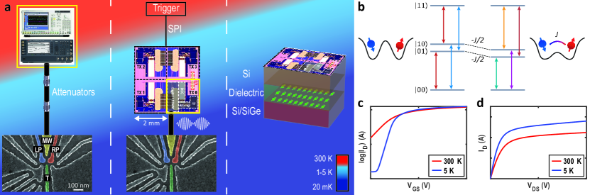
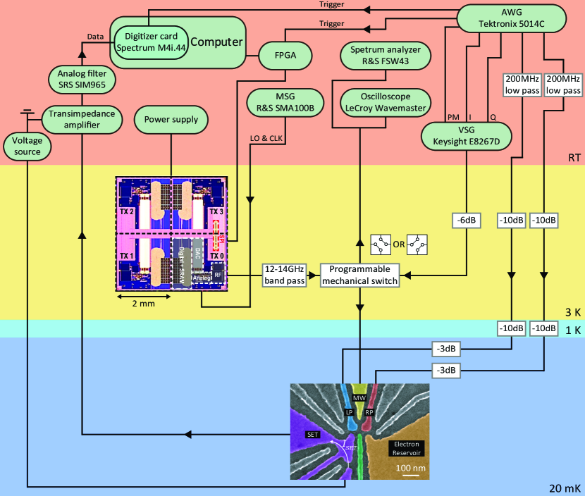
A practical quantum computer comprises two main building blocks – a quantum processor with millions of qubits and classical instrumentation to generate control signals (input) and to process readout signals (output) Vandersypen et al. (2017); Van Meter and Horsman (2013). A standard setup for semiconducting or superconducting qubits has the qubits operating in a dilution refrigerator at , while bulky microwave vector sources and arbitrary waveform generators are placed at room temperature and connected to the qubits via long cables and attenuators (Fig. 1a, left). This approach has recently enabled an experimental demonstration of the advantage of quantum computing over classical computing in a random circuit sampling experiment, that utilizes a superconducting quantum processor consisting of 53 qubits Arute et al. (2019). This system requires more than 200 coaxial control lines from room temperature to the quantum chip operated below . This brute-force approach to reach higher qubit numbers will soon hit its limits. A promising path forward is to bring the control electronics close to the quantum chip, at cryogenic temperatures Bardin et al. (2019); Patra et al. (2020a); Le Guevel et al. (2020); Bonen et al. (2018); Esmailiyan et al. (2020); Ekanayake et al. (2010); Mukhanov et al. (2019); Patra et al. (2018); Pauka et al. (2019); Xu et al. (2020). Here the challenge is that the power dissipation of the control electronics easily surpasses the typical cooling power of available at . Silicon spin qubits are well-positioned for co-integration with dissipative classical electronics, since they can be operated above Petit et al. (2020); Yang et al. (2020), where the cooling power is orders of magnitude higher (Fig. 1a, right). Therefore, an important next step is to design and implement a quantum control chip operating at 1-, and to test its overall performance in driving real qubits. In order to benchmark the limits of the controller, it is advantageous to keep the qubits at , where the qubits are most coherent and the demands on the controller are highest (Fig. 1a, middle).
A cryogenic quantum controller for practical quantum information processing must meet multiple criteria: a form factor compatible with integration in a cryogenic refrigerator; frequency multiplexing to facilitate scalability; low power consumption within the limit of refrigerator cooling power; sufficiently high output power to enable fast operations compared to the qubit coherence times; high signal-to-noise ratio (SNR) and spurious-free-dynamic-range (SFDR) for high-fidelity control; the ability to generate complex pulse shapes and perform a universal set of quantum operations; an integrated instruction set memory for the efficient execution of complex algorithms. All these requirements can be met by commercial CMOS circuits designed to operate at a few K.
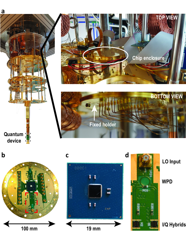
In this work, we utilize a quantum control chip operating at (cryo-controller, named Horse Ridge) and fabricated in Intel -FinFET low-power CMOS technology Patra et al. (2020a) to coherently control two electron spin qubits in a silicon double quantum dot cooled to . Extensive electrical characterization and benchmarking using the quantum processor show that the cryo-controller meets all the above criteria.
The specifications for the cryo-controller derive from the demands on the qubit control. Here we target qubits that can be resonantly controlled with drive frequencies in the 2- band, covering the typical resonance frequencies of both superconducting and spin qubits. The cryo-controller has four output ports, each with up to 32 frequency-multiplexed tones. Since the controller must dissipate minimal power and have a small form factor, we analyze in detail the signal specifications that are sufficient to achieve a gate fidelity van Dijk et al. (2020). Among other performance metrics, the most stringent ones dominating the architecture and power consumption of the controller are the SNR ( ) and SFDR ( ) for frequency-multiplexed control van Dijk et al. (2020).
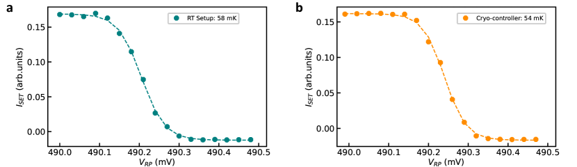
Further challenges arise in designing complex CMOS circuits at deep cryogenic temperatures. Key device characteristics such as the threshold voltage (Vth) and mobility () increase compared to room temperature, as seen in Fig. 1c, d Beckers et al. (2018). Moreover, the degradation of active device matching T Hart et al. (2020) and the improvement of the quality factor of on-chip passive components Patra et al. (2020b), necessitate careful characterization and modeling for circuits operated at cryogenic temperatures.
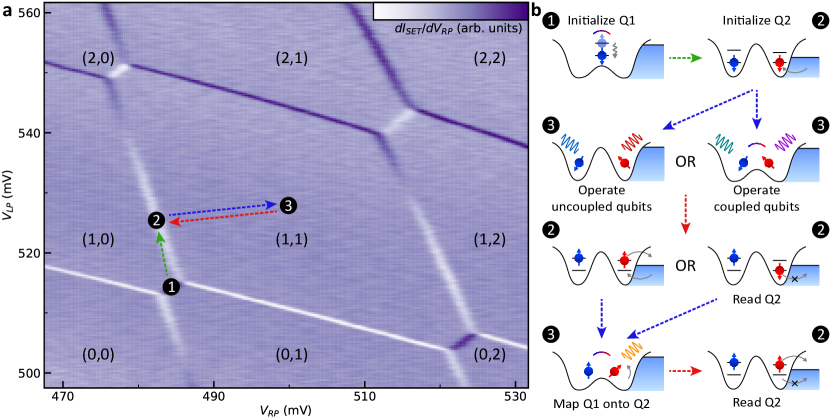
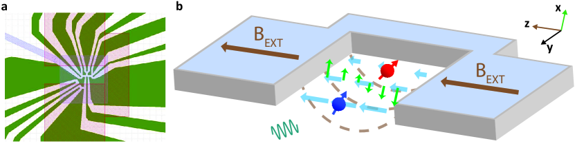
As a benchmark of performance, we use the cryo-controller to coherently control a two-qubit quantum processor. The quantum processor is made of a double quantum dot (DQD) electrostatically confined in a 28Si/SiGe heterostructure. By tuning the voltage on plunger gates LP and RP, two single electrons are locally accumulated underneath each gate, shown in blue and red in the scanning electron microscope (SEM) image in Fig. 1a. By applying an external magnetic field of , combined with the longitudinal magnetic field induced by a micro-magnet on top of the DQD (see Extended Data Fig. 7), we can encode the qubit states into the Zeeman split states of the two electrons, where spin-up is used as and spin-down is used as . The resonance frequencies of Qubit 1 (, underneath gate LP) and Qubit 2 (, underneath gate RP) are and , respectively. Rotations around the and axes are implemented by sending microwave bursts with the microwave phase controlling the rotation axis. The microwave bursts are applied to gate MW, which drives electric-dipole spin resonance (EDSR) enabled by the transverse magnetic field gradient from the micro-magnet Pioro-Ladrière et al. (2008), while the rotation around the axis (phase control) is achieved by changing the reference phase in the cryo-controller Vandersypen and Chuang (2005). The two-qubit interaction is mediated by the exchange coupling () between the two spins Petta et al. (2005), controlled by gate T. Its effect here is to shift the anti-parallel spin states down in energy Meunier et al. (2011). As a result, the resonance frequency of each qubit now depends on the state of the other qubit, allowing conditional operations on each qubit via narrow-band microwave bursts Zajac et al. (2017); Huang et al. (2019) (Fig. 1b). The corresponding four different frequencies can be individually addressed using frequency multiplexing. Both qubits are read out in single-shot mode Xue et al. (2020) (see Methods).
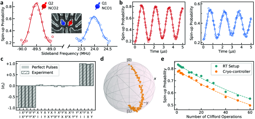
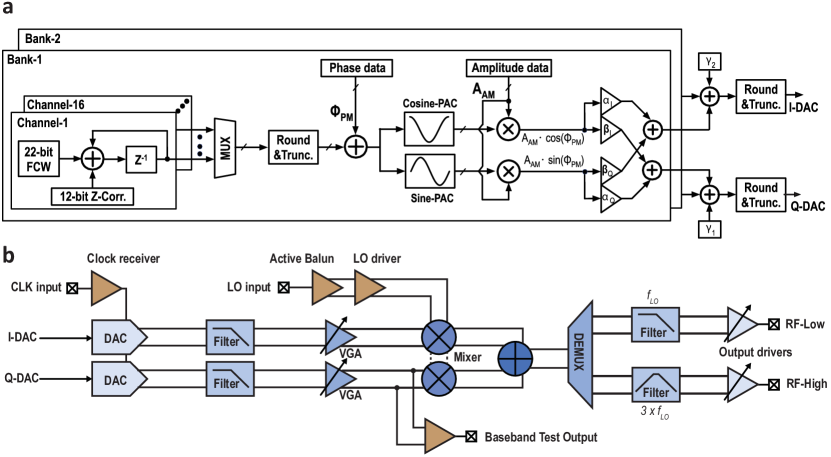
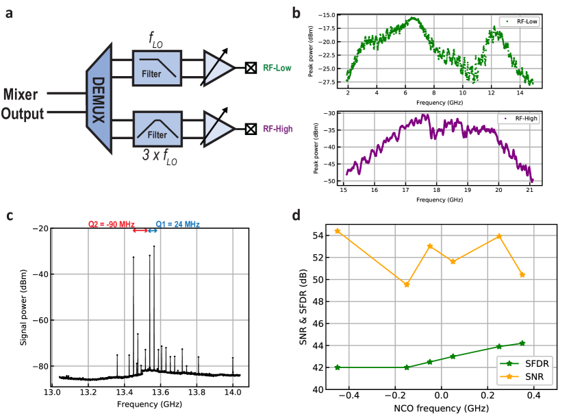
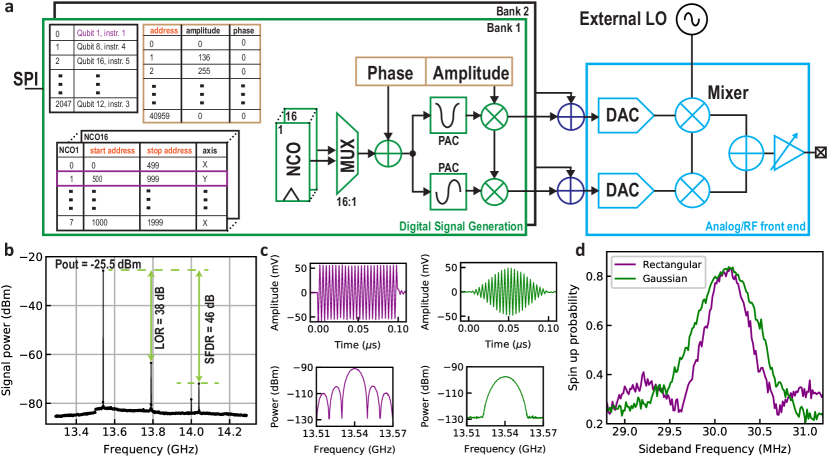
Figure 2 shows the system-level architecture of the cryo-controller, which consists of a digital signal generation unit with an analog/RF front-end. At the core of the digital signal generation, a numerically controlled oscillator (NCO) outputs a sequence of bit strings every clock period. This bit string encodes a phase that is intended to track the reference phase of one particular qubit. The output of 16 NCOs is multiplexed and fed to a phase-to-amplitude converter (PAC) to generate a sinusoidal (in-phase) and cosinusoidal (quadrature-phase) signal. The NCO phases are constructed via a phase accumulator, which increments the phase in steps determined by a digital frequency tuning word (FTW). The 22-bit FTWs in combination with the clock frequency of the phase accumulator gives a frequency resolution of .
The sine and cosine signals are amplitude and phase modulated using the envelope memory (orange box) containing up to 40960 points, each specifying an amplitude and phase value. An instruction table memory can store up to 8 different instructions per qubit/NCO by referring to start and stop addresses in the envelope memory. Finally, these instructions are listed in the instruction list to execute up to 2048 instructions from multiple instruction tables, initiated by a single external trigger. The output of two such banks, each generating a digital signal, are summed to simultaneously control two qubits, consequently increasing the number of supported (uncoupled) qubits from 16 to 32.
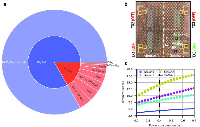
The generated digital signals are translated to the analog domain using high-speed digital-to-analog converters (DAC) and upconverted to the required qubit frequency using an I/Q mixer and an external local oscillator (LO). Finally, an output driver is incorporated to produce the required voltage amplitude (through a tunable gain of ) in the frequency range of 2 to , while driving the coaxial cable connecting to the qubits. Such a wide frequency and output power range allows the control of various solid-state qubits such as spin qubits and superconducting qubits. The controller dissipates with all the NCOs simultaneously operating at a clock frequency of (Digital Signal Generation: , Analog/RF front-end: ) (see Methods). This architecture is replicated 4 times in a die area of 2 (TX0-TX3 in Fig. 1) with an ability to control up to 4 32 frequency multiplexed qubits.
The purity of the generated signal can be quantified using the output signal spectrum shown in Fig. 2b. The generated signal has an SFDR of at in a bandwidth, excluding the residual LO leakage (see Extended Data Fig. 5 for a two-tone test). The noise floor is flat across the bandwidth, and the cryo-controller leaves the electron temperature of the quantum device unaffected (see Extended Data Fig. 8). The SNR is when integrating over , corresponding to the targeted maximum qubit Rabi frequency. Along with the low quantization noise and frequency noise, the output signal quality is predicted to achieve a single-qubit gate fidelity of 99.99%, assuming ideal qubits van Dijk et al. (2020). The amplitude and phase modulation capabilities of the controller allow the chip to generate arbitrary waveforms to precisely shape the spectral content of the pulse used to manipulate the qubits, as shown in Fig. 2c. In illustration, Fig. 2d shows the response of to a microwave burst with rectangular versus Gaussian envelope, both calibrated to invert the qubit state when the drive is on-resonance with the qubit.
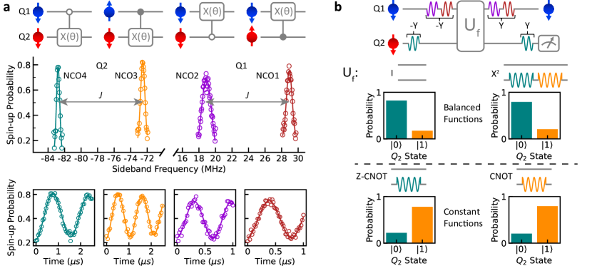
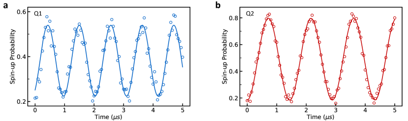
Next, we test the functionality of the cryo-controller for controlling uncoupled qubits. The LO frequency is set to . is then offset from the LO by and by . The qubit resonances are found by sweeping one single-sideband tone generated by one NCO (Fig. 3a), using the 22-bit FTW. Then we use one NCO from each bank to generate two tones on resonance with the two qubits and drive simultaneous Rabi oscillations on both qubits (Fig. 3b). Here a rectangular envelope is uploaded to the envelope memory, and saved as an instruction. The duration of the microwave burst is swept by updating the start or stop address of this instruction.
The pulses for single-qubit rotations are precisely calibrated using the AllXY sequence Reed (2013). In the AllXY experiment, 21 different pairs of single-qubit gates from the set are applied to a qubit initialized to . Here is the identity operation, and are rotations around the and axis respectively, and and are rotations. The final state -projection takes values from under perfect operations (shown as the gray shaded areas in Fig. 3c). Any miscalibration in the amplitude, frequency or phase of the pulse results in deviations from the ideal outcome (hatched bars in Fig. 3c). In addition, we reconstruct the trajectory of an gate by performing quantum-state tomography (QST) Altepeter et al. (2005) at incremental burst times of a rectangular microwave signal (Fig. 3d). The AllXY and QST results indicate that the single-qubit gate set is well calibrated, offering a good starting point for benchmarking the gate fidelity.
The gate fidelity is a crucial metric to express the performance of a quantum processor and its classical controller. We use single-qubit randomized benchmarking (RB) Knill et al. (2008); Magesan et al. (2012) to compare the performance of the cryo-controller with the conventional room temperature (RT) setup, which consists of an arbitrary waveform generator (Tektronix 5014C) and a vector signal generator (Keysight E8267D). A programmable microwave switch placed at the plate allows to conveniently alternate between the cryo-controller and the RT setup. In the RB experiment, sequences of increasing numbers of randomly selected Clifford operations are applied to the qubit (), followed by a final Clifford operation that returns the qubit to its initial state in the ideal case. For each data point in Fig. 3e, 32 different sequences are randomly sampled and each is repeated 200 times. Envelopes of all gates to be used are uploaded to the envelope memory, and saved as instructions. The random sequences are constructed by updating the instruction list. The instructions in the list are executed sequentially after an external trigger via the SPI in Fig. 2a is received. Exactly the same random sequences are used in an RB experiment using the RT setup. We find an average single-qubit gate fidelity of with the RT setup and with the cryo-controller (see Methods). The fidelities are consistently identical within the error bars and well above the threshold for fault-tolerance Fowler et al. (2012), with the infidelity limited by the qubit. These experiments demonstrate the high signal quality from the cryo-controller as well as its capability of generating complex sequences.
To further test the programmability of the cryo-controller, we use it to implement two-qubit logic in the quantum processor. Taking advantage of the frequency shift of each qubit conditional on the state of the other qubit (Fig. 1b), we use controlled-rotation () gates as the native two-qubit gates. These are achieved by frequency selective addressing Zajac et al. (2017); Huang et al. (2019), thus demanding 2 NCOs per qubit (see Methods). A -rotation at the higher or lower frequency implements the canonical controlled-NOT () gate or the zero-controlled-NOT (-) gate respectively, up to a single-qubit -rotation on the control qubit. Due to cross-talk, an additional phase correction in the form of a -rotation is needed. All rotations are implemented by updating the reference phase of the NCO (see Extended Data Fig. 3). Single-qubit gates are implemented by addressing both frequencies of the same qubit sequentially. Making use of four NCOs, we program the cryo-controller to run the two-qubit Deutsch–Josza algorithm, which determines whether a function gives constant or balanced outcomes Deutsch and Jozsa (1992). The two constant (balanced) functions that map one input bit on one output bit are implemented by the and - ( and ) operations. Here, we choose to be the output qubit and to be the input qubit. Fig. 4b shows the pulse sequence and the measurement results, where the constant (balanced) functions lead to a high probability for measuring the data qubit as (), as expected. This experiment highlights the ability to program the cryo-controller with arbitrary sequences of operations.
The cryo-controller allows for much more complex sequences, containing up to 2048 instructions for each of the four transmitters. Each instruction defines a microwave burst at one of 32 independent frequencies with an amplitude and phase profile that can be arbitrarily shaped. The cryo-controller can be conveniently embedded in existing micro-architectures and programmed via standard QASM variantsSvore et al. (2006). This quantum-classical architecture can thus be directly applied to multi-qubit algorithms and noisy intermediate-scale quantum devices Preskill (2018).
The versatile programmability combined with the signal quality allowing up to gate fidelities, the footprint of just , the power consumption of , the ability to integrate multiple transmitters on one die, and operation at , highlight the promise of cryo-controllers to address key challenges in building a large-scale quantum computer.
Optimized design of cryogenic CMOS circuits, e.g. the use of a narrower frequency band, can substantially reduce the power consumption (see Methods) and make it possible to work at or even lower temperatures. With the development of FinFET quantum dots and increased operating temperatures of spin qubits () Yang et al. (2020); Petit et al. (2020), it may be possible to fully integrate the quantum processor with the classical controller on-chip or by flip-chip technology, thus lifting a major roadblock in scaling.
Data availability
Data supporting this work will be uploaded to online repository.
Acknowledgements
This research was funded by the Intel Corporation. We acknowledge useful discussions with the members in the Spin Qubit team, the Cryo-CMOS team and Intel Corporation, and technical assistance by O. Benningshof, M. Sarsby, R. Schouten and R. Vermeulen.
Author contributions
X.X., B.P. and J.P.G.D performed the experiment. N.S. fabricated the quantum device. A.S. and G.S. grew the Si/SiGe heterostructure. A.C. contributed to the preparation of the experiment. X.X. and B.P. analysed the data. F.S., M.B., S.P., E.C. and L.M.K.V. conceived and supervised the project. X.X., B.P. and L.M.K.V. wrote the manuscript with input from all authors.
Competing interests
The authors declare no competing interests.
References
- Van Meter and Horsman (2013) R. Van Meter and C. Horsman, Communications of the ACM 56, 84 (2013).
- Vandersypen et al. (2017) L. M. K. Vandersypen, H. Bluhm, J. S. Clarke, A. S. Dzurak, R. Ishihara, A. Morello, D. J. Reilly, L. R. Schreiber, and M. Veldhorst, npj Quantum Inf. 3, 34 (2017).
- Patra et al. (2018) B. Patra, R. M. Incandela, J. P. Van Dijk, H. A. Homulle, L. Song, M. Shahmohammadi, R. B. Staszewski, A. Vladimirescu, M. Babaie, F. Sebastiano, et al., IEEE Journal of Solid-State Circuits 53, 309 (2018).
- Pauka et al. (2019) S. Pauka, K. Das, R. Kalra, A. Moini, Y. Yang, M. Trainer, A. Bousquet, C. Cantaloube, N. Dick, G. Gardner, et al., arXiv preprint arXiv:1912.01299 (2019).
- Geck et al. (2019) L. Geck, A. Kruth, H. Bluhm, S. van Waasen, and S. Heinen, Quantum Science and Technology 5, 015004 (2019).
- Watson et al. (2018) T. F. Watson, S. G. J. Philips, E. Kawakami, D. R. Ward, P. Scarlino, M. Veldhorst, D. E. Savage, M. G. Lagally, M. Friesen, S. N. Coppersmith, M. A. Eriksson, and L. M. K. Vandersypen, Nature 555, 633 (2018).
- Zajac et al. (2017) D. M. Zajac, A. J. Sigillito, M. Russ, F. Borjans, J. M. Taylor, G. Burkard, and J. R. Petta, Science 359, 439 (2017).
- Huang et al. (2019) W. Huang, C. Yang, K. Chan, T. Tanttu, B. Hensen, R. Leon, M. Fogarty, J. Hwang, F. Hudson, K. M. Itoh, A. Morello, A. Laucht, and A. S. Dzurak, Nature 569, 532 (2019).
- Deutsch and Jozsa (1992) D. Deutsch and R. Jozsa, Proceedings of the Royal Society of London. Series A: Mathematical and Physical Sciences 439, 553 (1992).
- Arute et al. (2019) F. Arute, K. Arya, R. Babbush, D. Bacon, J. C. Bardin, R. Barends, R. Biswas, S. Boixo, F. G. Brandao, D. A. Buell, et al., Nature 574, 505 (2019).
- Bardin et al. (2019) J. C. Bardin, E. Jeffrey, E. Lucero, T. Huang, S. Das, D. T. Sank, O. Naaman, A. E. Megrant, R. Barends, T. White, et al., IEEE Journal of Solid-State Circuits 54, 3043 (2019).
- Patra et al. (2020a) B. Patra, J. P. van Dijk, S. Subramanian, A. Corna, X. Xue, C. Jeon, F. Sheikh, E. Juarez-Hernandez, B. P. Esparza, H. Rampurawala, et al., in 2020 IEEE International Solid-State Circuits Conference-(ISSCC) (IEEE, 2020) pp. 304–306.
- Le Guevel et al. (2020) L. Le Guevel, G. Billiot, X. Jehl, S. De Franceschi, M. Zurita, Y. Thonnart, M. Vinet, M. Sanquer, R. Maurand, A. G. Jansen, et al., in 2020 IEEE International Solid-State Circuits Conference-(ISSCC) (IEEE, 2020) pp. 306–308.
- Bonen et al. (2018) S. Bonen, U. Alakusu, Y. Duan, M. Gong, M. Dadash, L. Lucci, D. Daughton, G. Adam, S. Iordănescu, M. Pǎşteanu, et al., IEEE Electron Device Letters 40, 127 (2018).
- Esmailiyan et al. (2020) A. Esmailiyan, H. Wang, M. Asker, E. Koskin, D. Leipold, I. Bashir, K. Xu, A. Koziol, E. Blokhina, and R. B. Staszewski, IEEE Solid-State Circuits Letters (2020).
- Ekanayake et al. (2010) S. R. Ekanayake, T. Lehmann, A. S. Dzurak, R. G. Clark, and A. Brawley, IEEE Transactions on Electron Devices 57, 539 (2010).
- Mukhanov et al. (2019) O. Mukhanov, A. Kirichenko, C. Howington, J. Walter, M. Hutchings, I. Vernik, D. Yohannes, K. Dodge, A. Ballard, B. Plourde, et al., in 2019 IEEE International Electron Devices Meeting (IEDM) (IEEE, 2019) pp. 31–2.
- Xu et al. (2020) Y. Xu, F. Unseld, A. Corna, A. Zwerver, A. Sammak, D. Brousse, N. Samkharadze, S. Amitonov, M. Veldhorst, G. Scappucci, et al., arXiv preprint arXiv:2005.03851 (2020).
- Petit et al. (2020) L. Petit, H. Eenink, M. Russ, W. Lawrie, N. Hendrickx, S. Philips, J. Clarke, L. Vandersypen, and M. Veldhorst, Nature 580, 355 (2020).
- Yang et al. (2020) C. H. Yang, R. Leon, J. Hwang, A. Saraiva, T. Tanttu, W. Huang, J. C. Lemyre, K. W. Chan, K. Tan, F. E. Hudson, et al., Nature 580, 350 (2020).
- van Dijk et al. (2020) J. P. G. van Dijk, B. Patra, S. Pellerano, E. Charbon, F. Sebastiano, and M. Babaie, IEEE Transactions on Circuits and Systems I: Regular Papers , 1 (2020).
- Beckers et al. (2018) A. Beckers, F. Jazaeri, and C. Enz, IEEE Journal of the Electron Devices Society 6, 1007 (2018).
- T Hart et al. (2020) P. A. T Hart, M. Babaie, E. Charbon, A. Vladimirescu, and F. Sebastiano, IEEE Journal of the Electron Devices Society 8, 797 (2020).
- Patra et al. (2020b) B. Patra, M. Mehrpoo, A. Ruffino, F. Sebastiano, E. Charbon, and M. Babaie, IEEE Journal of the Electron Devices Society 8, 448 (2020b).
- Pioro-Ladrière et al. (2008) M. Pioro-Ladrière, T. Obata, Y. Tokura, Y.-S. Shin, T. Kubo, K. Yoshida, T. Taniyama, and S. Tarucha, Nat. Phys. 4, 776 (2008).
- Vandersypen and Chuang (2005) L. M. K. Vandersypen and I. L. Chuang, Rev. Mod. Phys. 76, 1037 (2005).
- Petta et al. (2005) J. R. Petta, A. C. Johnson, J. M. Taylor, E. A. Laird, A. Yacoby, M. D. Lukin, C. M. Marcus, M. P. Hanson, and A. C. Gossard, Science 309, 2180 (2005).
- Meunier et al. (2011) T. Meunier, V. Calado, and L. Vandersypen, Physical Review B 83, 121403 (2011).
- Xue et al. (2020) X. Xue, B. D’Anjou, T. F. Watson, D. R. Ward, D. E. Savage, M. G. Lagally, M. Friesen, S. N. Coppersmith, M. A. Eriksson, W. A. Coish, et al., Physical Review X 10, 021006 (2020).
- Reed (2013) M. Reed, Entanglement and quantum error correction with superconducting qubits (Lulu. com, 2013).
- Altepeter et al. (2005) J. B. Altepeter, E. R. Jeffrey, and P. G. Kwiat, Advances in Atomic, Molecular, and Optical Physics 52, 105 (2005).
- Knill et al. (2008) E. Knill, D. Leibfried, R. Reichle, J. Britton, R. B. Blakestad, J. D. Jost, C. Langer, R. Ozeri, S. Seidelin, and D. J. Wineland, Physical Review A 77, 012307 (2008).
- Magesan et al. (2012) E. Magesan, J. M. Gambetta, and J. Emerson, Physical Review A 85, 042311 (2012).
- Fowler et al. (2012) A. G. Fowler, M. Mariantoni, J. M. Martinis, and A. N. Cleland, Physical Review A 86, 032324 (2012).
- Svore et al. (2006) K. M. Svore, A. V. Aho, A. W. Cross, I. Chuang, and I. L. Markov, Computer 39, 74 (2006).
- Preskill (2018) J. Preskill, Quantum 2, 79 (2018).
- Srinivasa et al. (2013) V. Srinivasa, K. C. Nowack, M. Shafiei, L. Vandersypen, and J. M. Taylor, Physical review letters 110, 196803 (2013).
Methods
Programming the cryo-controller.
The setup (Extended Data Fig.1) contains a field-programmable gate array (FPGA) that configures the cryo-controller (e.g. FTW), programs the various memories inside the cryo-controller (e.g. envelope memories, instruction tables and instruction lists), and controls the start of the execution of the instruction list. The FPGA is connected to the host PC, which sends the data that needs to be uploaded to the cryo-controller over the SPI. The instruction list integrated in the cryo-controller does not support classical instructions that allow for e.g. branching or wait statements, as required for performing certain qubit experiments and for synchronization with other equipment. Therefore, switching between different instruction lists and synchronization with the rest of the equipment, is controlled by two trigger lines from the AWG to the FPGA. The application of the execute trigger starts the execution of the instruction list that is programmed in the cryo-controller, for performing repeated measurements. The application of the sweep trigger loads the next instruction list from the FPGA SRAM into the cryo-controller’s instruction list.
Power budget. The high power consumption of the digital circuitry of the cryo-controller is caused due to the lack of clock gating in registers (memory), thus causing them to continuously operate instead of just during the read/write cycle. This could easily be reduced by further optimizations (e.g. by replacing more registers with SRAM memory and by adding clock gating), that were not yet included in the first generation cryo-controller. Based on the simulation with clock-gating, the power consumption of the digital circuitry should be lower than instead of in the current design. Moreover, this chip was designed to address both transmons and spin qubits and hence an ultra-wide output frequency range was supported i.e. 2 to . Once the qubit frequency is fixed within a few GHz range, the power consumption of the analog circuitry can be significantly reduced to limit the power consumption to instead of .
Si/SiGe heterostructure.
The quantum processor is made by gate-confined quantum dots in a 28Si/SiGe heterostructure, which is grown using a reduced pressure chemical vapor deposition reactor (ASM Epsilon 2000). First, a Si1-xGex buffer layer (with linearly increasing from 0 to 0.3) is grown on top of a p-type natural Si wafer, followed by a strain-relaxed Si0.7Ge0.3 layer. Then a isotopically purified tensile-strained 28Si (with residual 29Si concentration) quantum well is grown, followed by a strain-relaxed Si0.7Ge0.3 barrier layer. Finally a sacrificial Si cap is grown on top.
Quantum dot device fabrication On top of the heterostructure, a AlOx layer is deposited using atomic-layer deposition (ALD), followed by a Al metal film, which is patterned using electron beam lithography in order to define a first gate layer, which shapes the potential landscape. Next another AlOx layer is deposited, followed by a Al layer which uniformly covers the quantum dot area. Finally, a Co film is deposited and patterned into a micro-magnet (see Extended Data Fig. 7).
Qubit readout.
The readout scheme is described in Extended Data Fig.6. After each operation sequence, is measured by spin-selective tunneling to the electron reservoir, where a spin-up () electron can tunnel out and a spin-down () electron is blockaded from tunneling out. Such a spin-to-charge conversion changes the charge occupancy in the quantum dot conditional on the spin state. This in turn changes the current signal in an adjacent capacitively coupled single-electron-transistor (SET). Single-shot readout of the qubit state can be done by thresholding the current signal through the SET Xue et al. (2020). The post-measurement state in this readout protocol is the state, serving as reinitialization. is tuned to be only weakly coupled to the SET, which serves as the electron reservoir for . This is to minimize the back-action from the SET, but also makes it less efficient to readout by spin-selective tunneling to the SET. Therefore, with reinitialized, a gate is applied to map the state of onto . Then is readout by measuring again Xue et al. (2020). The readout fidelity of is mainly limited by the thermal broadening of the electron reservoir, and the readout fidelity of is limited by both the error in the gate and in the readout of . Thus the readout visibility of is lower than .
Readout error removal.
In the AllXY experiments and in the implementation of the Deutsch-Jozsa algorithm, the readout probabilities of are normalized with calibrated readout fidelities .
After preparing in , can be calibrated directly through the measured spin-down probability, and is calibrated through the measured spin-up probability after a spin-flip operation (the spin-flip fidelity is above ). Based on the measured state probabilities in the AllXY and Deutsch-Jozsa experiments, , the actual state probabilities can be reconstructed by , where
| (1) |
Error sources.
In the simultaneous Rabi oscillation experiment (Fig.3), we attribute the visible decays in both curves to the residual exchange coupling between the two qubits. Simultaneous Rabi oscillations recorded (in this case using the RT setup) over larger numbers of oscillations show beating patterns. These patterns are well reproduced by numerical models of the spin evolution in the presence of a finite residual exchange coupling. Such a beating effect looks like a decay in the beginning. It is absent in the individually driven Rabi oscillation (Extended Data Fig.9). In the two-qubit experiments shown in Fig.4, the decay in the controlled-rotation Rabi oscillations and the finite visibilities in the Deutsch-Jozsa algorithm are largely attributed to charge noise. With the exchange coupling turned on, as needed for two-qubit gates, the energy levels are much more sensitive to charge noise.
Quantum state tomography.
In the QST experiment, the qubit state is measured by projecting it onto the axes. The projection on the axis is measured by direct readout of the spin state, while the projections on other axes are measured by applying a , , or gate, which are calibrated by the AllXY experiment, before the readout. The trajectory of the qubit state in the course of a gate can be reconstructed by performing QST at incremental burst times of a rectangular microwave signal (Fig.3.c.), with each measurement repeated 1,000 times. To visualize the qubit state in the Bloch sphere, we remove the readout error from the data. Since error removal can lead to unphysical states such as data points outside the Bloch sphere, a maximum likelihood estimation is implemented to find the closest physical state of the qubit Altepeter et al. (2005).