Dimensional Crossover Tuned by Pressure in Layered Magnetic NiPS3
Abstract
Layered magnetic transition-metal thiophosphate NiPS3 has unique two-dimensional (2D) magnetic properties and electronic behavior. The electronic band structure and corresponding magnetic state are expected to sensitive to the interlayer interaction, which can be tuned by external pressure. Here, we report an insulator-metal transition accompanied with magnetism collapse during the 2D-3D crossover in structure induced by hydrostatic pressure. A two-stage phase transition from monoclinic () to trigonal () lattice is identified by simulation and confirmed by high-pressure XRD and Raman data, corresponding to a layer by layer slip mechanism along the -axis. Temperature dependence resistance measurements and room temperature infrared spectroscopy show that the insulator-metal transition occurs near 20 GPa as well as magnetism collapse, which is further confirmed by low temperature Raman measurement and theoretical calculation. These results establish a strong correlation among the structural change, electric transport, and magnetic phase transition and expand our understandings about the layered magnetic materials.
I INTRODUCTION
Dimensionality plays an important role to determine the structure, electronic and magnetic properties in most condensed matter systems. The layered materials with van der Waals (vdW) interaction provide a good platform for us to study how the phases and interactions evolve when the material is tuned from the two-dimensional (2D) limit to the there-dimensional (3D) state. Since graphene was first stripped from the natural graphite by Andre Geim and Konstantin Novoselov Geim2007 , a large number of 2D materials with atomic thickness then became the new favorite of the scientific community, such as 2D transition metal dichalcogenides tmd01 ; tmd02 ; tmd03 . Recently, the layered transition metal trichalcogenides (MPX3; M = Fe, Ni, Mn, etc.; X = S and Se) in antiferromagnetic (AFM) state Gong2017 ; Lee2016 ; Li2014 ; Lancon2016 ; Wildes2015 ; Wildes2012 ; Wildes2006 ; Wildes1998 ; Wildes2017 have also attracted tremendous interests due to their tunable electronic properties and the potential applications in magnetic materials and spintronic devices LiX2014 ; LiX2013 . These compounds are connected by vdW interactions and bring both magnetism and correlated electron physics to the playground of vdW materials BREC1986 ; Chittari2016 ; Rabu2003 ; Wang2018 .
The MPX3 compounds are typical 2D antiferromagnetic materials, the axial distortion of the MX6 octahedron is likely to produce anisotropy that can dominate the spin dimension (Ising, XY or Heisenberg model). For example, FePS3 uses the Ising model, NiPS3 uses the XY model, and MnPS3 uses the Heisenberg model Lee2016 ; Wildes2015 ; Joy1992 . The magnetic exchange of these compounds is mainly super-exchange interaction, and the sign and property of the super-exchange interaction depend on the M-S-M angle of the metal ion and the electron occupancy rate. Also, some MPX3 materials exhibit more than one magnetic phase transition with changes in temperature. Therefore, it is of great significance to extend the performance of these MPX3 materials to the field of spintronics.
In addition to magnetism, MPX3 compounds also have rich electronic properties. Many of these materials are Mott or Charge-Transfer insulators with a wide range of electronic band gaps from 0.25 eV to 3.5 eV Wang2018 ; Ouvrard1985 ; Du2016 ; Kuo2016 ; Kurita1989 ; Whangbo1985 ; Piacentini1982 ; Brec1979 , and can be tuned by changing parameters. For example, in the MoS2 system, the monolayer MoS2 changes from a direct bandgap to an indirect bandgap semiconductor under high pressure, while the bulk material MoS2 undergoes a metallic transition under high pressure Fan2015 . In addition, there are many research groups that have conducted many high-pressure studies on MPX3 and reported or predicted the insulator-metal transition Tsurubayashi2018 ; Haines2018 ; Wang2016 ; WangY2018 ; Evarestov2020 ; Kim2019 ; Coak2019 ; Coak2020 .
With the rapid development of 2D materials, high pressure has already become a very important parameter to tune the states of materials and study their fundamental physical properties, such as structural phase transition, electronic behavior and even magnetism. For example, as mentioned above, at sufficient pressure, the band gap of many materials can close and experience insulator-metal transition. Many novel and rich physical properties can be obtained through pressure regulation. MPX3 provide a good platform for us to study how the phases and interactions evolve when the system is tuned from the 2D limit to the 3D state through pressure.
In this paper, we report a systematic study on the structure, electronics and magnetism of NiPS3 under pressure. A two-stage phase transition which undergoes 2D-3D crossover is found in bulk NiPS3 by calculations, high-pressure XRD and Raman measurements. During the whole structure phase transition, the interlayer distance changes more obviously compared with other unit cell parameters. The first structural phase transition occurs at about 15 GPa, and the new structure has the same space group () as the ambient structure with a a/3 slip along the a-axis. Meanwhile, the magnetism collapse and insulator-metal transition in pressurized bulk NiPS3 are observed around 20 GPa through high-pressure resistance, infrared, Raman and other measurements. The second structural phase transition occurs at about 27 GPa with a a/2 slip along the a-axis, and its space group becomes , exhibiting 3D behavior.
II RESULTS AND DISCUSSION
II.1 Structure phase transition
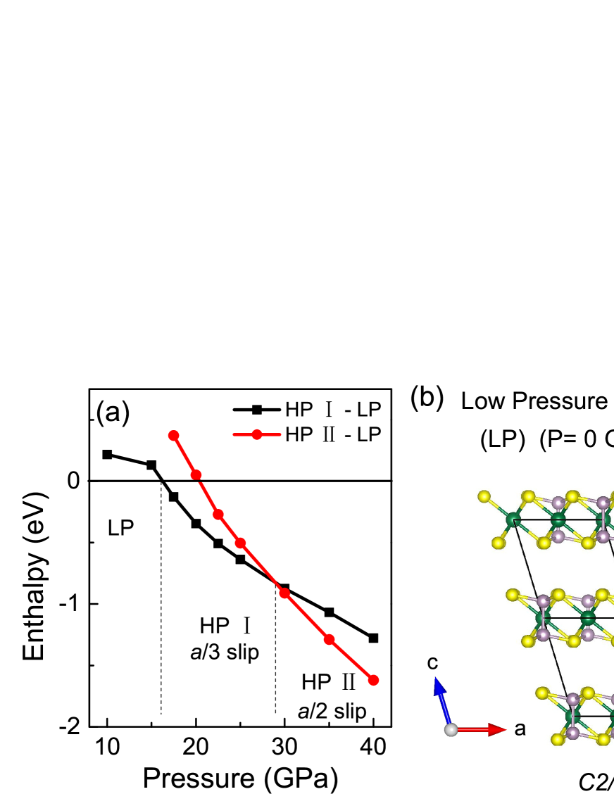
At ambient condition, NiPS3 has a layered structure in monoclinic (, No. 12) symmetry Ouvrard1985 ; Klingen1968 . In order to explore the structure changes of NiPS3 under pressure, we have performed a detailed simulation using a double cell along the -axis [see Fig. 1(b)]. Several possible structures are considered via a layer by layer slip mechanism along the -axis. Fig. 1(a) displays the enthalpy change of different phases relative to the original monoclinic phase under pressure. According to the principle of lowest energy, we confirm three phases up to 40 GPa. We temporarily define the structure at 0 GPa as low pressure phase (LP); the phase at 20 GPa is defined as high pressure phase I (HP-I); the one at 30 GPa is defined as high pressure phase II (HP-II). The LP phase is existing below 16 GPa, HP-II phase is more faverable above 28 GPa, and HP-I phase is located between 1628 GPa, showing as an intermediate state. Fig. 1(b) displays the crystal structure of the LP phase of NiPS3. Viewed along b-axis, we can see the well separated sandwich layers associated with weak interlayer vdW interaction. The HP-I structure has a a/3 slip along a-axis [Fig. 1(c)]. The slip between the ab planes with pressure is feasible as the planes are only weakly bound by vdW forces and they can slide easily over one another. LP and HP-I phases are isostructural phase transition, they have the same space group . The HP-II structure has a a/2 slip along a-axis [Fig. 1(d)]. This phase transition leads to the closely related (No. 162) trigonal structure which adopts a higher symmetry in paramagnetic state (see Fig. 5). From LP to HP-II phase of the entire structure evolution process, we can clearly see a 2D-3D crossover, relative to the intermediate state of HP-I phase. These results suggest a two-stage phase transition process from monoclinic () to trigonal () structure via a layer by layer slip mechanism under pressure.
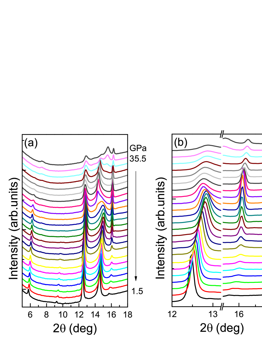
To verify the calculated structure model, we have conducted a high-pressure XRD measurement of NiPS3. The diffraction patterns evolved with pressure are presented in Fig. 2(a). From the diffraction patterns, two distinct phase transitions can be observed near 15 GPa and 27 GPa, respectively. The first phase transition begins at approximately 15 GPa and completely transitions to another phase around 20 GPa. The second phase transition occurs at approximately 27 GPa. For the first phase transition, there is a new diffraction peak develops while other peak disappears. The evolution of the peak around 14.5∘ begins to occur near 15 GPa. It evolves into a new peak at about 20 GPa and then becomes another phase upon this pressure. In addition to this change, the other two diffraction peaks 12.5∘ and 16.0∘ [see Fig. 2(b)] also have corresponding responses around 15 GPa. Below 15 GPa, the peak around 12.5∘ gradually moves to a higher angle as the pressure gradually increases, while above 15 GPa, it moves to a lower angle first, and then continues to move to a high angle as the pressure increases; On the other hand, below 15 GPa, the intensity of the peak around 16.0∘ increases with increasing pressure, while above 15 GPa, the intensity of this diffraction peak weakens with increasing pressure. Based on the above phenomena, we believe that NiPS3 undergoes the first phase transition occurs around 15 GPa. The phase transition around 15 GPa has also been verified in the Raman scattering measurement (see Fig. S1 in the Supplementary Material sm00 ). For the second phase transition at approximately 27 GPa, there are also new diffraction peaks develop while one peak disappears. The diffraction peak around 6∘ disappears, and two new peaks appear around 6.5∘ and 14.5∘ at approximately 27 GPa. Our experimental results are well consistent with the calculated results shown in Fig. 1(a).
Fig. 2(c-f) shows the experimental cell parameters as a function of applied pressure for the LP and HP phases of NiPS3. From Fig. 2(c-e) we can see that all the lattice parameters , and are in a consistent trend when they are below 10 GPa. This interval is the LP phase. In contrast, in the pressure range of 10-15 GPa, the change trend of the unit cell parameters slow down with increasing pressure. This interval should be a transition interval. All unit cell parameters , and above 15 GPa change suddenly, and the volume gradually decreases with increasing pressure [Fig. 2(f)]. The lattice parameter a decreases by 0.5% [Fig. 2(c)], b increases by 2.1% [Fig. 2(d)], and c decreases by 5.4% [Fig. 2(e)]. Compared with the unit cell parameters a and b, the unit cell parameter c which includes the vdW gap decreases rather rapidly with the pressure . So the effect of pressure on the interlayer is greater. In this interval, a structural phase transition should occur, which is a HP-I phase. This HP-I and LP phase adopt the same space group of . Thus, monoclinic unit cells with space group were adopted for cell parameter fitting for NiPS3. However, because the XRD peaks above 30 GPa are weaker, fewer and wider, it is difficult to fit. So the fitting data above 30 GPa is not given. In addition, because 27-30 GPa belongs to the transition interval, so in this interval we still use the HP-I structure for fitting. It can be found from the fitting result that the change of the unit cell parameters are the same as the result given by the simulation calculation. The obvious decline of the interlayer distance also provides more favorable conditions for 2D-3D crossover.
II.2 Insulator-Metal transition
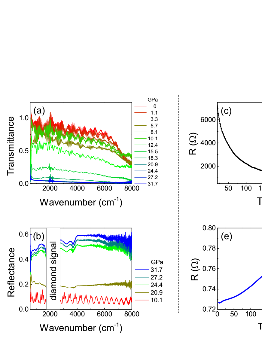
The infrared measurement has important guiding significance for us to understand the high-pressure electronic behavior of materials, therefore, we performed infrared measurement on bulk NiPS3 under high pressure. The high-pressure infrared measurement includes two parts: transmittance and reflectance. The transmittance of the insulator is close to 1, and the transmittance of metal is close to 0. As can be seen from Fig. 3(a), under ambient pressure, the transmittance of NiPS3 is close to 1, which is an insulator. As the pressure gradually increases, the transmittance of NiPS3 gradually decreases, indicating that its band gap is gradually decreasing, and the insulator gradually transitions to metal. When the pressure increases to 20.9 GPa, the transmittance of NiPS3 is close to 0, and it becomes a metal. As the pressure continues to increase, the transmittance of NiPS3 no longer changes. In addition, as the reflectance increases, the metallicity will increase, so we continue to observe the metallization process through reflectance. By observing the change of reflectance under different pressures, we also got the same conclusion. From Fig. 3(b), we can see that the reflectance is small and the interference is strong at 10 GPa. As the pressure gradually increases, the reflectance increases, and the spectrum gradually smoothes. At around 20.9 GPa, the spectrum becomes very smooth , suggesting that there is no interference between top surface and bottom surface of NiPS3 crystal, which is a typical character of metallic behavior. The reflectance increases significantly when pressure reaches 24.4 GPa, above which reflectance tends to be stable. The signal around 2000 cm-1 is the absorption signal of diamond. In addition, we also clearly observed the metallization process by optic reflection picture of NiPS3. For details, see Fig. S2 in Supplementary Material sm00 .
In order to verify the accuracy of the metallization behavior, we measured the resistance of bulk NiPS3 under high pressure. Temperature-dependent resistance under different pressures are plotted in Fig. 3(c-f). A transition from insulator to metal is seen around 20 GPa. From Fig. 3(c-f) we can see that as the pressure gradually increases, the resistance is gradually suppressed, and there is a decrease in magnitude. For details, see Fig. S3 in Supplementary Material sm00 . Through Fig. 3(c-f) we can see the metallization process of NiPS3. At 14.2 GPa the data appears as an insulator and to be an intermediate state at 17.2 GPa [Fig. 3(c) and (d)]. Continue to increase pressure to about 20.2 GPa [Fig. 3(e)], the sample completely metallized. We continue to increase the pressure until 24.7 GPa [Fig. 3(f)], NiPS3 still maintains a good metal behavior. This measurement confirms the result of infrared measurement.
The above measurement methods have clearly confirmed that the bulk NiPS3 will undergo an insulator-metal phase transition under pressure. At present, related articles predict that monolayer MPX3 will still maintain insulator or semiconductor behavior under pressure without metallization Xiang2016 . That is, the bulk NiPS3 exhibits 3D characteristics that are different from "pure" 2D (monolayer) NiPS3. We speculate that the difference in behavior between bulk NiPS3 and monolayer NiPS3 may be caused by the interlayer interaction.
II.3 Magnetic property
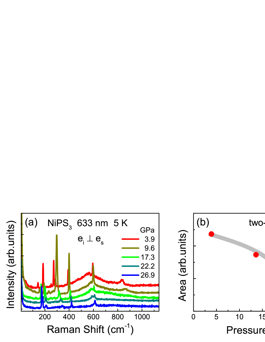
In order to verify the correlation between the magnetic properties and the interlayer interaction of NiPS3, we have measured and calculated the magnetic properties of NiPS3. By performing temperature-dependent Raman scattering measurements on bulk NiPS3 from 5.6 to 300 K at ambient pressure, we discovered the two-magnon signal of NiPS3 centered at 550 cm-1. Details can be seen in Fig. S4 in the Supplementary Material sm00 . Consistent with the results measured in other articles Rosenblum1999 ; KimK2019 . In order to investigate the effect of pressure on two-magnon, we conducted the Raman measurements of bulk NiPS3 in the cross-polarization configuration under different pressures at the low temperature of 5 K [Fig. 4(a)]. In the cross-polarization configuration, some phonons, especially those superimposed on the two-magnon, are suppressed, so the two-magnon signal in this configuration is clearer. From these data we can find that the two-magnon signal was gradually suppressed and shift towards higher frequencies as the pressure increased. The two-magnon signal became very small around 22 GPa and was totally suppressed around 27 GPa. Such a rule is also satisfied under different polarization configurations and different temperatures. For details, see Fig. S5 and S6 in Supplementary Material sm00 . In order to quantitatively describe the change of magnetism with pressure, we fitted the data in Fig. 4(a) and gave the two-magnon area of bulk NiPS3 under different pressures [Fig. 4(b)]. From Fig. 4(b), we can see that the area of the two-magnon decreases with increasing pressure. When the pressure reaches about 27 GPa, the magnetism completely disappears.
In addition to the experimental results, we also calculated the magnetic moment of NiPS3 under pressures with an intralayer AFM structure Rao1992 . In Fig. 4(c), the calculated moments on Ni sites are plotted as a function of pressure up to 40 GPa for bulk NiPS3. We can see that the moments on Ni sites are quickly deceased from 15 GPa and quenched around 22 GPa. Its behavior is consistent with the trend of the area of the two-magnon changing with pressure in Fig. 4(b). For comparison, we have also calculated the magnetic moments for the monolayer NiPS3 (just extend the interlayer spacing in a double cell along the c-axis) at each pressure. As shows in Fig. 4(c), the moments on Ni sites almost show a linear decreasing behavior and are well kept up to 40 GPa, indicating that the AFM state is expected to be stable in the monolayer limit under high pressure. Similar to the electrical behavior, the magnetic behavior of bulk NiPS3 also shows 3D characteristics which different from "pure" 2D (monolayer) NiPS3. These results suggest that the magnetic moments are strongly influenced by the interlayer interaction.
To get the best understanding of interlayer interaction, we have calculated the total and projected electronic density of states (DOS) at 20 GPa for both bulk and monolayer NiPS3 (see Fig. S7 in Supplementary Material sm00 ). It is shown that the bulk NiPS3 at 20 GPa has a metallic behavior, while the monolayer NiPS3 has a semiconducting behavior with a band gap of 0.43 eV. These results suggest the magnetic moments and electronic property (metallic or semiconducting) are strongly correlated with the interlayer distance.
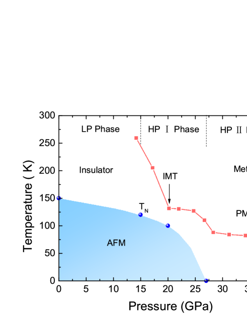
II.4 Phase diagram
Fig. 5 shows the temperature-pressure phase diagram of bulk NiPS3. Two structural transitions are clearly visible at 15 GPa and 27 GPa, respectively. The structure below 15 GPa is the LP phase. The phase between 15-27 GPa is the HP-I phase, a transition region of 2D-3D. The structure above 27 GPa is the HP-II phase. It can be seen from the phase diagram that the insulator-metal transition happens at the mixed phase (HP-I phase). The red point in the figure is the resistance under different pressures at 300 K. As the pressure increases, the resistance suddenly decreases and metallizes around 20 GPa. The AFM-PM transition ccurs at the junction of HP-I and HP-II phases. As can be seen, TN is suppressed progressively to 0 K at 27 GPa, above which the antiferromagnetic disappears.
III CONCLUSION
In summary, we report the close correlation among the structure, electronic and magnetic properties of NiPS3 driven by external hydrostatic pressure. Dimensional crossover appears not just in structural phase transition, but also in electronic behavior and magnetism evolution. Two new phases HP-I and HP-II of NiPS3 are proposed by calculations and confirmed by high-pressure XRD experiment. The change from LP to HP-I structure is accompanied with a a/3 slip along the a-axis. The space group is still , which is an isostructural phase transition. Compared with the LP phase, the cell parameters change suddenly in this phase. In particular, the change in the interlayer distance is most obvious. As a result, the magnetism of bulk NiPS3 are gradually suppressed, while the magnetism of the monolayer NiPS3 remains stable. At the same time, bulk NiPS3 completed the transition from insulator to metal in this phase, while monolayer NiPS3 is still a semiconductor under high pressure. The structural change from HP-I to HP-II is accompanied with a a/2 slip along the a-axis. In the meanwhile, a 2D-3D crossover occurred in structure, forming a new space group . NiPS3 maintains metallic behavior in this phase. At this time, due to structural changes, the magnetism of NiPS3 is completely suppressed, and the magnetic moment on Ni sites becomes 0. Both electrical and magnetic properties show 3D characteristics different from their "pure" 2D behavior under pressure. These results suggest these properties are strongly correlated with the interlayer distance. The properties of this compound under pressure are very rich, which provides a good model for the future research on the physical properties of other layered magnetic materials.
ACKNOWLEDGMENTS
This study was supported by the National Key R&D Program of China under Grant Nos 2016YFA0401503, 2018YFA0305700, 2017YFA0302904 and 2016YFA0300500, the National Natural Science Foundation of China under Grant No. 11575288, 11974387, U1932215, U1930401 and 11774419, the Strategic Priority Research Program and Key Research Program of Frontier Sciences of the Chinese Academy of Sciences (Grant Nos. XDB33000000, XDB25000000 and Grant No. QYZDBSSW-SLH013) and the Youth Innovation Promotion Association of Chinese Academy of Sciences under Grant No 2016006. ADXRD measurements were performed at 4W2 High Pressure Station, Beijing Synchrotron Radiation Facility (BSRF), which is supported by Chinese Academy of Sciences (Grant KJCX2-SW-N20, KJCX2-SW-N03). The work is partially carried out at High-pressure synergetic measurement station of synergetic extreme condition user facility.
APPENDIX: MATERIALS AND METHODS
III.1 Sample synthesis
Single crystals of NiPS3 were grown by chemical vapor transport method (CVT). The crystal naturally cleaves along the (001) surface, forming NiPS3 flakes weakly bonded by van der Waals force. Amount of high-purity elements nickel, phosphorus, and sulfur were mixed in a stoichiometric mole ratio of 1:1:3 (around 1 g in total) and iodine (about 0.123 g) was used as a transport agent. These raw materials were sealed into a quartz ampoule with a length of about 16 cm and an external diameter of 13 mm, and the pressure inside the quartz ampoule was pumped down to 110-4 Torr. Put the quartz ampoule into a two-zone furnace (680-720 ∘C) and heat it for two weeks. Cool the quartz ampoule down to room temperature, and bulk crystals can be obtained on the top of the quartz ampoule.
III.2 The high-pressure measurements
The high-pressure four-probe electrical resistance, X-ray powder diffraction (XRD) and Raman measurements were performed in diamond anvil cells (DACs). The DAC made of BeCu alloy with two opposing anvils was used to generated high pressure. Diamond anvils with 300 m culets were used for the measurements. In these experiments, a thin single crystal sample of 10*50*100 m was loaded into the sample chamber (D = 100 m hole) in a rhenium gasket with c-BN insulating layer, and a ruby ball is loaded to serve as internal pressure standard. The ruby fluorescence method was used to determine the pressure. The high-pressure four-probe electrical resistance measurement is carried out at High-pressure synergetic measurement station of synergetic extreme condition user facility Yu2018 .
The high-pressure XRD measurements were performed at beamline 4W2 at Beijing Synchrotron Radiation Facility. A monochromatic X-ray beam with a wavelength of 0.6199 Å was used for the measurements. Silicone oil was used as pressure-transmitting medium.
The high-pressure and temperature-dependent Raman spectra were collected using a HR800 spectrometer (Jobin Yvon) equipped with a liquid-nitrogen-cooled charge-coupled device (CCD) and volume Bragg gratings, for which micro-Raman backscattering configuration was adopted. A 633 nm laser was used, with a spot size of 5 m focused on the sample surface. The laser power was maintained at approximately 1.4 mW to avoid overheating during measurements. KBr was used as pressure-transmitting medium.
The high-pressure infrared experiments were performed at room temperature on a Bruker VERTEX 70v infrared spectroscopy system with HYPERION 2000 microscope. A thick NiPS3 single crystal was used and KBr was used as pressure medium. The spectra were collected in transmission and reflective mode in the range of 600-8000 cm-1 with a resolution of 4 cm-1 through a 3030 m2 aperture.
III.3 Computational methods
The calculations are performed using the Vienna simulation package (VASP) Kresse1996 with the projector augmented wave method Blochl1994 and spin polarized generalized gradient approximation Perdew1996 for the exchange-correlation energy. The valence states 3d94s1 for Ni, 3s23p3 for P, and 3s23p4 for S are used with the energy cutoff of 550 eV for the plane wave basis set. To simulate the interlayer interaction, a 112 supercell (in AA stacking including 8 NiPS3 formula) is used with a vdW correction Tkatchenko2009 . An intralayer zigzag antiferromagnetic structure Rao1992 is set with the interlayer ferromagnetic coupling. The Brillouin zone is sampled with a 744 Monkhorst-Pack special k-point grid. Throughout our calculations with or without pressure, convergence criteria employed for both the electronic self-consistent relaxation and the ionic relaxation were set to 10-6 eV and 0.01 eV/A for energy and force, respectively.
References
- (1) A. K. Geim and K. S. Novoselov, The Rise of Graphene, Nat. Mater. 6, 183 (2007).
- (2) M. Chhowalla, H. S. Shin, G. Eda, L.-J. Li, K. P. Loh, and H. Zhang, The chemistry of two-dimensional layered transition metal dichalcogenide nanosheets, Nat. Chem. 5, 263 (2013).
- (3) D. Jariwala, V. K. Sangwan, L. J. Lauhon, T. J. Marks, and M. C. Hersam, Emerging device applications for semiconducting two-dimensional transition metal dichalcogenides, ACS Nano 8, 1102 , (2014).
- (4) S. Manzeli, D. Ovchinnikov, D. Pasquier, O. V. Yazyev, and A. Kis, 2D transition metal dichalcogenides, Nat. Rev. Mater. 2017, 2, 17033 (2017).
- (5) C. Gong et al., Discovery of Intrinsic Ferromagnetism in Two-Dimensional van der Waals Crystals, Nature 546, 265 (2017).
- (6) J. U. Lee, S. Lee, J. H. Ryoo, S. Kang, T. Y. Kim, P. Kim, C. H. Park, J. G. Park, and H. Cheong, Ising-Type Magnetic Ordering in Atomically Thin FePS3, Nano. Lett. 16, 7433 (2016).
- (7) X. Li and J. Yang, CrXTe3 (X = Si, Ge) Nanosheets: Two Dimensional Intrinsic Ferromagnetic Semiconductors, J. Mater. Chem. C 2, 7071 (2014).
- (8) D. Lançon, H. C. Walker, E. Ressouche, B. Ouladdiaf, K. C. Rule, G. J. McIntyre, T. J. Hicks, H. M. Rønnow, and A. R. Wildes, Magnetic Structure and Magnon Dynamics of the Quasi-Two-Dimensional Antiferromagnet FePS3, Phys. Rev. B 94, 214407 (2016).
- (9) A. R. Wildes et al., Magnetic Structure of the Quasi-Two-Dimensional Antiferromagnet NiPS3, Phys. Rev. B 92, 224408 (2015).
- (10) A. R. Wildes, K. C. Rule, R. I. Bewley, M. Enderle, and T. J. Hicks, The Magnon Dynamics and Spin Exchange Parameters of FePS3, J. Phys. Condens. Matter 24, 416004 (2012).
- (11) A. R. Wildes, H. M. Rønnow, B. Roessli, M. J. Harris, and K. W. Godfrey, Static and Dynamic Critical Properties of the Quasi-Two-Dimensional Antiferromagnet MnPS3, Phys. Rev. B 74, 094422 (2006).
- (12) A. Wildes, B. Roessli, B. Lebech, and K. Godfrey, Spin Waves and the Critical Behaviour of the Magnetization in MnPS3, J. Phys. Condens. Matter 10, 6417 (1998).
- (13) A. R. Wildes, V. Simonet, E. Ressouche, R. Ballou, and G. J. McIntyre, The Magnetic Properties and Structure of the Quasi-Two-Dimensional Antiferromagnet CoPS3, J. Phys. Condens. Matter 29, 455801 (2017).
- (14) X. Li, X. Wu, and J. Yang, Half-Metallicity in MnPSe3 Exfoliated Nanosheet with Carrier Doping, J. Am. Chem. Soc. 136, 11065 (2014).
- (15) X. Li, T. Cao, Q. Niu, J. Shi, and J. Feng, Coupling the Valley Degree of Freedom to Antiferromagnetic Order, Proc. Natl. Acad. Sci. 110, 3738 (2013).
- (16) R. BREC, Review on Structural and Chemical Properties of Transition Metal Phosphorous Trisulfides MPS3, Solid State Ionics 22, 3 (1986).
- (17) B. L. Chittari, Y. Park, D. Lee, M. Han, A. H. MacDonald, E. Hwang, and J. Jung, Electronic and Magnetic Properties of Single-Layer MPX3 Metal Phosphorous Trichalcogenides, Phys. Rev. B 94, 184428 (2016).
- (18) P. Rabu and M. Drillon, Layered Organic-Inorganic Materials: A Way towards Controllable Magnetism, Adv. Eng. Mater. 5, 189 (2003).
- (19) F. Wang et al., New Frontiers on van der Waals Layered Metal Phosphorous Trichalcogenides, Adv. Funct. Mater. 28, 1802151 (2018).
- (20) P. A. Joy and S. Vasudevan, Magnetism in the Layered Transition-Metal Thiophosphates MPS3 (M = Mn, Fe, and Ni), Phys. Rev. B 46, 5425 (1992).
- (21) G. Ouvrard, R. Brec, and J. Rouxel, Structural Determination of Some MPS3 Layered Phases (M = Mn, Fe, Co, Ni and Cd), Mat. Res. Bull. 20, 1181 (1985).
- (22) K. Z. Du, X. Z. Wang, Y. Liu, P. Hu, M. I. Utama, C. K. Gan, Q. Xiong, and C. Kloc, Van der Waals Stacking, Wide-Range Band Gap, and Raman Study on Ultrathin Layers of Metal Phosphorus Trichalcogenides, ACS Nano 10, 1738 (2016).
- (23) C. T. Kuo et al., Exfoliation and Raman Spectroscopic Fingerprint of Few-Layer NiPS3 Van der Waals Crystals, Sci. Rep. 6, 20904 (2016).
- (24) N. Kurita and K. Nakao, Band Structure of Magnetic Layered Semiconductor NiPS3, J. Phys. Soc. Jpn. 58, 232 (1989).
- (25) M. Whangbo, R. Brec, G. Ouvrard, and J. Rouxel, Reduction Sites of Transition-Metal Phosphorus Trichalcogenides, MPX3, Inorg. Chem. 24, 2459 (1985).
- (26) M. Piacentini, F. Khumalo, C. Olson, J. Anderegg, and D. Lynch, Optical Transitions, XPS, and Electronic States in NiPS3, Chem. Phys. 65, 289 (1982).
- (27) R. Brec, D. M. Schleich, G. Ouvrard, A. Louisy, and J.Rouxel, Physical Properties of Lithium Intercalation Compounds of the Layered Transition Chalcogenophosphates, Inorg. Chem. 18, 1814 (1979).
- (28) X. Fan, C. H. Chang, W. T. Zheng, J.-L. Kuo, and D. J. Singh, The Electronic Properties of Single-Layer and Multilayer MoS2 under High Pressure, J. Phys. Chem. C 119, 10189 (2015).
- (29) M. Tsurubayashi, K. Kodama, M. Kano, K. Ishigaki, Y. Uwatoko, T. Watanabe, K. Takase, and Y. Takano, Metal-Insulator Transition in Mott-Insulator FePS3, AIP Adv. 8, 101307 (2018).
- (30) C. R. S. Haines, M. J. Coak, A. R. Wildes, G. I. Lampronti, C. Liu, P. Nahai-Williamson, H. Hamidov, D. Daisenberger, and S. S. Saxena, Pressure-Induced Electronic and Structural Phase Evolution in the van der Waals Compound FePS3, Phys. Rev. Lett. 121, 266801 (2018).
- (31) Y. Wang et al., Pressure-Driven Cooperative Spin-Crossover, Large-Volume Collapse, and Semiconductor-to-Metal Transition in Manganese(II) Honeycomb Lattices, J. Am. Chem. Soc. 138, 15751 (2016).
- (32) Y. Wang et al., Emergent Superconductivity in an Iron-Based Honeycomb Lattice Initiated by Pressure-Driven Spin-Crossover, Nat. Commun. 9, 1914 (2018).
- (33) R. A. Evarestov and A. Kuzmin, Origin of Pressure-Induced Insulator-to-Metal Transition in the van der Waals Compound FePS3 from First-Principles Calculations, J. Comput. Chem. 41, 1337 (2020).
- (34) H. S. Kim, K. Haule, and D. Vanderbilt, Mott Metal-Insulator Transitions in Pressurized Layered Trichalcogenides, Phys. Rev. Lett. 123, 236401 (2019).
- (35) M. J. Coak et al., Isostructural Mott Transition in 2D Honeycomb Antiferromagnet V0.9PS3, npj Quantum Mater. 4, 38 (2019).
- (36) M. J. Coak et al., Tuning Dimensionality in van-der-Waals Antiferromagnetic Mott Insulators TMPS3, J. Phys. Condens. Matter 32, 124003 (2020).
- (37) W. Klingen, G. Eulenberger, and H. Hahn, Über Hexathio- und Hexase1enohypodiphosphate vom Typ MP2X6, Die Naturwissenschaften 55, 229 (1968).
- (38) See Supplemental Material for (1) pressure dependence of Raman spectra; (2) optic reflection pictures under different pressures; (3) resistance plotted against temperature under different pressures; (4) changes of two-magnon signal with temperature in different channels; (5) the behavior of the two-magnon with pressure at 5 K; (6) the behavior of the two-magnon with pressure at different temperatures; and (7) DOSs for bulk and monolayer NiPS3.
- (39) H. Xiang, B. Xu, Y. Xia, J. Yin, and Z. Liu, Tunable Electronic Structures in MPX3 (M = Zn, Cd; X = S, Se) Monolayers by Strain Engineering, RSC Adv. 6, 89901 (2016).
- (40) S. S. Rosenblum and R. Merlin, Resonant Two-Magnon Raman Scattering at High Pressures in the Layered Antiferromagnetic NiPS3, Phys. Rev. B 59, 6317 (1999).
- (41) K. Kim et al., Suppression of Magnetic Ordering in XXZ-Type Antiferromagnetic Monolayer NiPS3, Nat. Commun. 10, 345 (2019).
- (42) R. R. Rao and A. Raychaudhuri, Magnetic Studies of a Mixed Antiferromagnetic System Fe1-xNiPS3, J. Phys. Chem. Solids 53, 577 (1992).
- (43) X. Yu, F. Li, Y. Han, F. Hong, C. Jin, Z. He, and Q. Zhou, High-pressure synergetic measurement station (HP-SymS), Chinese Phys. B 27, 070701 (2018).
- (44) G. Kresse and J. Furthmüller, Efficient Iterative Schemesfor ab Initio Total-Energy Calculations Using a Plane-Wave Basis Set, Phys. Rev. B 54, 11169 (1996).
- (45) P. E. Blöchl, Projector Augmented-Wave Method, Phys. Rev. B 50, 17953 (1994).
- (46) J. P. Perdew, K. Burke, and M. Ernzerhof, Generalized Gradient Approximation Made Simple, Phys. Rev. Lett. 77, 3865 (1996).
- (47) A. Tkatchenko and M. Scheffler, Accurate Molecular van der Waals Interactions from Ground-State Electron Density and Free-Atom Reference Data, Phys. Rev. Lett. 102, 073005 (2009).