Electron-phonon coupling of epigraphene at millikelvin temperatures
Abstract
We investigate the basic charge and heat transport properties of charge neutral epigraphene at sub-kelvin temperatures, demonstrating nearly logarithmic dependence of electrical conductivity over more than two decades in temperature. Using graphene’s sheet conductance as in-situ thermometer, we present a measurement of electron-phonon heat transport at mK temperatures and show that it obeys the dependence characteristic for clean two-dimensional conductor. Based on our measurement we predict the noise-equivalent power of of epigraphene bolometer at the low end of achievable temperatures.
Epitaxial graphene on SiC substrate (epigraphene) is an attractive scalable Emtsev ; Virojanadara technology for high-quality graphene electronics Tzalenchuk ; Lara-Avila1 ; He1 . Using a recently reported doping technique He2 , epigraphene doped close to the Dirac point has shown to have great potential for astronomy-oriented terahertz (THz) wave detection, acting as a hot electron bolometric mixer (g-HEB) in heterodyne detection Lara-Avila1 . For g-HEBs, understanding the energy relaxation processes in the material is crucial as it directly impacts the device design, and is paramount to achieve high sensitivities and large device bandwidths desired in astronomical observations Klapwijk . In general, decreasing the thermal relaxation rate and heat capacity improves the sensitivity of bolometers and calorimeters roope ; JP1 ; this observation has triggered a number of studies on electron-phonon heat transport in graphene at sub-kelvin temperatures efetov ; FG ; Finkelstein ; XuDu ; Schwab . For epigraphene, little is known about relaxation processes, particularly when the material is doped close to the Dirac point and in the millikelvin temperature range, conditions at which g-HEBs are expected to perform better. Previous studies of the energy relaxation mechanisms of epigraphene have been mostly limited to samples at high carrier densities and at liquid helium temperatures Baker ; Huang , or on micron-sized devices where thermalization of hot carriers occurred via the metallic contacts (i.e. diffusion cooling) Lara-Avila1 .
Here we present a study of energy relaxation in charge neutral epigraphene devices fitted with superconducting contacts, which act as thermal barriers that prevent heat leak from the contacts, thus enabling the study of energy relaxation processes in the graphene-silicon carbide system. We use in-situ thermometry down to sub- mK temperatures by measuring the sheet conductance of epigraphene Hall bar devices as they are locally heated by injecting current through Hall probes. This method provides a built-in thermometer, and its made possible thanks to the strong temperature dependence of resistance in lowly-doped epigraphene He2 ; Lara-Avila1 .
Epigraphene was grown on a 4H-SiC chips ( mm2), which were encased in a graphite crucible and heated using RF heating to around in an inert argon atmosphere of 1 bar Virojanadara . Transmission mode microscopy was used to ensure that the samples had high ( %) monolayer coverage Yager . Device fabrication utilized standard electron beam lithography techniques, described in detail elsewhere Yager2 . In short, epigraphene was patterned into Hall bar structure by oxygen plasma etching and superconducting metallic contacts were prepared with nm-thick aluminium contacts using a nm-thick adhesion layer of titanium. This is a proven technique to make transparent electrical contacts to graphene Heersche ; Mizuno . The metallic layers were deposited using physical vapour deposition using electron beam evaporation. The finished device was spin-coated with molecular dopants and the final carrier density was tuned close to charge neutrality by annealing at He2 . In order to test the device quality, initial DC electrical characterization was performed using quantum Hall measurements in a PPMS (Physical Property Measurement System from Quantum design) liquid helium cryostat ( K) with a superconducting magnet providing fields up to T. Sub-kelvin measurements were performed in a dilution refrigerator.
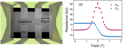
Figure 1(a) shows an optical micrograph of the doped epigraphene Hall bar used for our study, with channel length m and width m. Quantum Hall measurements at K were used to verify the quality of the devices (Fig. 1(b)). The sample shows fully developed quantum Hall effect, with vanishing longitudinal resistance and quantized transverse resistance . This proves that the sample is of high quality monolayer epigraphene with spatially homogenous doping He2 ; Cho ; Tiwari . The device is p-doped, with carrier density of cm-2, and mobility cmVs.
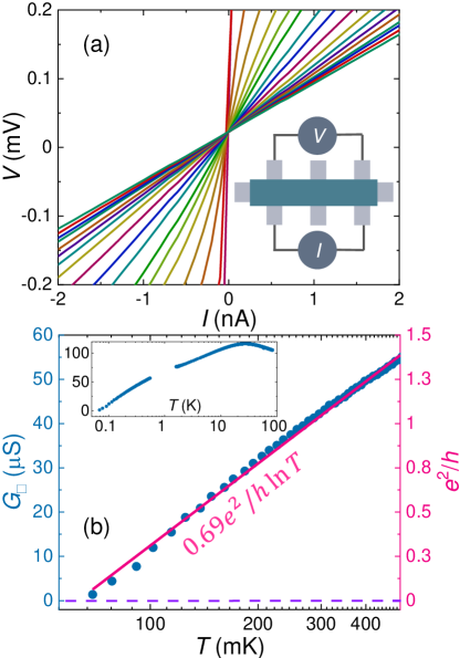
In Fig. 2(a) we show the current-voltage () characteristics measured in a dilution refrigerator at various temperatures ranging from about mK up to mK. The four-probe configuration for these measurements is shown in the inset of Fig. 2(a). The temperature dependence of zero-bias differential sheet conductance of the device is seen in Fig. 2(b), extracted from the average slope of the curve over a current range of a few pA around zero current. The vertical scale on the right (shown in blue color) is the sheet conductance expressed in units of the conductance quantum . The inset of Fig. 2(b) shows the temperature dependence of the sheet conductance in a wider temperature range. Data in the two separate ranges of temperature were measured using different set-ups. We observe approximately logarithmic-in-temperature dependence of the sheet conductance of graphene, , with S, where is the elementary charge, and is the Planck’s constant. The slope of the logarithmic term quantifies the strength of the quantum corrections in the material, and for this p-doped sample, , higher than reported for n-doped samples Lara-Avila1 . Studies in magnetic field would be required to verify if a higher is the result of enhanced electron-electron interactions or quantum interference effects in p-doped samples.
For thermal characterization of the device, we have considered four contributions when analysing the local thermal balance of the epigraphene structure. These are (i) the thermal conductance from epigraphene to the phonon bath , (ii) the lateral thermal conductance along the epigraphene sheet , (iii) the thermal conductance of the substrate partly shunting thermally the epigraphene (), and finally (iv) the thermal conductance to the superconducting leads () to which the Hall bar structure is connected. For an ideal measurement of epigraphene properties only, the two first ones ought to dominate and the two others should not contribute to the heat currents. Yet, as we argue below, our measurements, together with estimates of substrate material properties, and assuming that the Wiedemann-Franz law is approximately valid for epigraphene, the shunting effect (iii) exceeds the thermal conductance along the epigraphene sheet by several orders of magnitude.
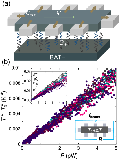
In the measurements of the hot electron effect in the epigraphene device, depicted in Fig. 3(a), the Joule power generated by the bias current leads to an increase of the electronic temperature of graphene, which is measured through monitoring the sheet conductance of the material. With superconducting contacts acting as heat barriers, the heat flow through the contacts is negligible, i.e. and the only energy relaxation pathway in the system is through the phonon bath [i.e. item (i)] . Figure 3(b) is a collection of such measurements in the temperature range 170 mK to 306 mK, showing that the heat flux from the electron system at temperature to the phonon bath (at constant bath temperature ) follows the law
| (1) |
with , and WK-4m-2. This power law is consistent with theoretical predictions for graphene in the clean limit FG ; XuDu , and with previous reports in highly n-doped epigraphene ( cm-2 ) and at temperatures up to K Baker ; Huang . For comparison, the inset of Fig. 3(b) shows the dependence of electron-phonon heat current for graphene in the dirty-limit. We conclude that describes the experiment more closely, with data at various temperatures collapsing better on the same line.
The electrical conductance across the Hall bar, e.g. between two adjacent Hall probes with a distance of m, is (see Fig. 2b). Using Wiedemann-Franz law we obtain W/K for the thermal conductance in this geometry at K. Here is the Lorenz number. It is then evident that the electron-phonon conductance dominates and shunts the system thermally as under the same conditions W/K for the area under the heater. Since the thermal conductance of the 3D structure is large, we conclude that the role of is negligible in our measurements.
The thermal characterization allows to calculate the noise-equivalent power (NEP), an important figure of merit of a bolometer. In the limit where this figure is determined by fundamental energy fluctuations, it assumes value . In our case from the electron-phonon measurement, mK, and m2 we obtain . This is still not record-low because of the large area in our sample and relatively high . In order to improve the NEP, one needs to reduce the area of the detector and operate it at lower . One can realistically make m2 and operate at about 10 mK. In this case the projected , which would outperform the current experimental state-of-the-art roope . Although here we do not present heat transport data below mK, we believe that lower measurements are feasible: applying a moderate magnetic field of mT perpendicular to graphene sheet restores the conductance of it down to mK.
In summary, we have demonstrated sensitive in-situ thermometry by measuring the sheet conductance of the epigraphene sheet down to sub- mK temperatures, providing a way for sensitive calorimetry with a built-in thermometer. The coupling of the epigraphene electrons to the phonon bath dies off more slowly with decreasing temperature than in metal films versus JPrmp ; therefore the advantage in operating at the very low temperatures is not quite that obvious in case of epigraphene as compared to metals, where furthermore the proximity superconductivity can be used for enhancement of sensitivity. Yet, the extremely small heat capacity of the epigraphene sheets at low temperatures leads to very fast thermal relaxation times of the order of ps, making, together with in-situ thermometry and weak , epigraphene bolometer an attractive choice for terahertz applications.
Acknowledgements.
This work was jointly supported by the Swedish Foundation for Strategic Research (SSF) (Nos. GMT14-0077 and RMA15-0024), Chalmers Excellence Initiative Nano, and European Union’s Horizon 2020 research and innovation programme under Marie Sklodowska-Curie Grant Agreement No 766025. This work was performed in part at Myfab Chalmers. We acknowledge the facilities and technical support of Otaniemi research infrastructure for Micro and Nanotechnologies (OtaNano). We thank the Russian Science Foundation (Grant No. 20-62-46026) for supporting the work.References
- (1) K. v Emtsev, A. Bostwick, K. Horn, J. Jobst, G.L. Kellogg, L. Ley, J.L. McChesney, T. Ohta, S. a Reshanov, J. Röhrl, E. Rotenberg, A.K. Schmid, D. Waldmann, H.B. Weber, and T. Seyller, Nature Materials 8, 203 (2009).
- (2) C. Virojanadara, M. Syväjarvi, R. Yakimova, L. Johansson, a. Zakharov, and T. Balasubramanian, Phys. Rev. B 78, 245403 (2008).
- (3) A. Tzalenchuk, S. Lara-Avila, A. Kalaboukhov, S. Paolillo, M. Syväjärvi, R. Yakimova, O. Kazakova, T.J.B.M. Janssen, V. Fal’ko, and S. Kubatkin, Nature Nanotechnology 5, 186 (2010).
- (4) S. Lara-Avila, A. Danilov, D. Golubev, H. He, K.H. Kim, R. Yakimova, F. Lombardi, T. Bauch, S. Cherednichenko, and S. Kubatkin, Nature Astronomy 3, (2019).
- (5) H. He, S. Lara-Avila, K.H. Kim, N. Fletcher, S. Rozhko, T. Bergsten, G. Eklund, K. Cedergren, R. Yakimova, Y.W. Park, A. Tzalenchuk, and S. Kubatkin, Metrologia 56, 045004 (2019).
- (6) H. He, K.H. Kim, A. Danilov, D. Montemurro, L. Yu, Y.W. Park, F. Lombardi, T. Bauch, K. Moth-Poulsen, T. Iakimov, R. Yakimova, P. Malmberg, C. Müller, S. Kubatkin, and S. Lara-Avila, Nat. Commun. 9, 3 (2018).
- (7) T. M. Klapwijk, and A. V. Semenov, IEEE Trans. Terahertz Sci. Technol. 7, 627–648 (2017).
- (8) Kokkoniemi, R. et al. Nanobolometer with ultralow noise equivalent power, Commun. Phys. 2, 124 (2019).
- (9) Bayan Karimi, Fredrik Brange, Peter Samuelsson and Jukka P. Pekola, Reaching the ultimate energy resolution of a quantum detector, Nat. Comm. 11, 367 (2020).
- (10) Dmitri K. Efetov, Ren-Jye Shiue, Yuanda Gao, Brian Skinner, Evan D. Walsh, Hyeongrak Choi, Jiabao Zheng, Cheng Tan, Gabriele Grosso, Cheng Peng, James Hone, Kin Chung Fong, and Dirk Englund, Nature Nanotech 13, 797 (2018).
- (11) Francesco Vischi, Matteo Carrega, Alessandro Braggio, Federico Paolucci, Federica Bianco, Stefano Roddaro, and Francesco Giazotto, Phys. Rev. Appl. 13, 054006 (2020).
- (12) I.V. Borzenets, U. C. Coskun, H. T. Mebrahtu, Yu.V. Bomze, A. I. Smirnov, and G. Finkelstein, Phys. Rev. Lett. 111, 027001 (2013)
- (13) Xu Du, Daniel E. Prober, Heli Vora, and Christopher B. Mckitterick, Graphene 2D Mater. 1, 1 (2014).
- (14) Kin Chung Fong, Emma E. Wollman, Harish Ravi, Wei Chen, Aashish A. Clerk, M. D. Shaw, H. G. Leduc, and K. C. Schwab, Phys. Rev. X 3, 041008 (2013).
- (15) A. M. R. Baker, J. A. Alexander-Webber, T. Altebaeumer, S. D. McMullan, T. J. B. M. Janssen, A. Tzalenchuk, S. Lara-Avila, S. Kubatkin, R. Yakimova, C. -T. Lin, L. -J. Li, and R. J. Nicholas, Phys. Rev. B 87, 045414 (2013).
- (16) J. Huang, J. A. Alexander-Webber, T. J. B. M. Janssen, A. Tzalenchuk, T. Yager, S. Lara-Avila, S. Kubatkin, R. L. Myers-Ward, V. D. Wheeler, D. K. Gaskill, and R. J. Nicholas, J. Phys. Condens. Matter 27, 164202 (2015).
- (17) T. Yager, A. Lartsev, S. Mahashabde, S. Charpentier, D. Davidovikj, A. Danilov, R. Yakimova, V. Panchal, O. Kazakova, A. Tzalenchuk, S. Lara-Avila, and S. Kubatkin, Nano Letters 13, 4217 (2013).
- (18) A. Tzalenchuk, S. Lara-Avila, K. Cedergren, M. Syväjärvi, R. Yakimova, O. Kazakova, T. Janssen, K. Moth-Poulsen, T. Bjørnholm, S. Kopylov, V. Fal’ko, S. Kubatkin, Solid State Communications 151, 1094 (2011).
- (19) H.B. Heersche, P. Jarillo-Herrero, J.B. Oostinga, L.M.K. Vandersypen, and A.F. Morpurgo, Nature 446, 56 (2007).
- (20) N. Mizuno, B. Nielsen, and X. Du, Nat. Commun. 4, (2013).
- (21) S. Cho and M.S. Fuhrer, Physical Review B - Condensed Matter and Materials Physics 77, 8 (2008).
- (22) R.P. Tiwari and D. Stroud, Physical Review B - Condensed Matter and Materials Physics 79, 1 (2009).
- (23) S. Lara-Avila, A. Tzalenchuk, S. Kubatkin, R. Yakimova, T.J.B.M. Janssen, K. Cedergren, T. Bergsten, and V. Fal’Ko, Phys. Rev. Lett. 107, (2011).
- (24) Francesco Giazotto, Tero T. Heikkilä, Arttu Luukanen, Alexander M. Savin, and Jukka P. Pekola, Rev. Mod. Phys. 78, 217 (2006).