Two-dimensional chiral stacking orders in quasi-one-dimensional charge density waves
Abstract
Chirality manifests in various forms in nature. However, there is no evidence of the chirality in one-dimensional charge density wave (CDW) systems. Here, we have explored the chirality among quasi-one-dimensional CDW ground states with the aid of scanning tunneling microscopy, symmetry analysis, and density functional theory calculations. We discovered three distinct chiralities emerging in the form of two-dimensional chiral stacking orders composed of degenerate CDW ground states: right-, left-, and nonchiral stacking orders. Such chiral stacking orders correspond to newly introduced chiral winding numbers. Furthermore, we observed that these chiral stacking orders are intertwined with chiral vortices and chiral domain walls, which play a crucial role in engineering the chiral stacking orders. Our findings suggest that the unexpected chiral stacking orders can open a way to investigate the chirality in CDW systems, which can lead to diverse phenomena such as circular dichroism depending on chirality.
Chirality or handedness exists everywhere in nature and plays a significant role in all branches of the natural sciences including chemistry, biology, mathematics, and physics Hyde et al. (1996). In spin- or pseudospin-ordered states, chirality manifests in various forms including magnetic chiral solitons in chiral magnets, vortices or skyrmions in thin magnetic layers, and topological monopoles in Weyl semimetals Braun (2012); Nagaosa and Tokura (2013); Armitage et al. (2018). Such richness is quite natural because of the vector order parameter in spin/pseudospin systems. In contrast, it is hard to find chirality in charge-ordered states since their order parameter has a scalar nature. A decade ago, two-dimensional (2D) -TiSe2 was proposed as the first charge density wave (CDW) system with a three-dimensional (3D) real-space chiral stacking order due to inversion symmetry breaking Ishioka et al. (2010). Such a chiral order of -TiSe2 has been investigated in terms of chiral phase transition Castellan et al. (2013) and optically induced gyrotropic electronic order Xu et al. (2020). However, a recent sophisticated scanning tunneling microscopy (STM) investigation revealed that the intrinsic 3D chiral order (without optical induction) of -TiSe2 is not allowed due to its preserved inversion symmetry between two adjacent layers Hildebrand et al. (2018). Thus, the existence of the intrinsic chiral order in 2D CDW remains elusive. Furthermore, there has been no report regarding its one-dimensional (1D) counterpart that exhibits 2D chiral orders in 1D CDW.
Recently, topological solitons with chirality are realized in quasi-1D CDW atomic wires consisting of indium (In) atoms on Si(111) Kim and Yeom (2012); Cheon et al. (2015); Kim et al. (2017). Although the solitons are found to exhibit unusual topological properties such as topology, charge fractionalization, and topological algebraic operation between them Cheon et al. (2015); Kim et al. (2017), their CDW ground states have not been explored in terms of chirality or chiral order. In this system, mirror symmetry is spontaneously broken as soon as CDW arises. Since such broken symmetry makes CDW ground states to be geometrically chiral, this quasi-1D CDW system might show chiral CDW orders in real space.
In this Rapid Communication, we carefully investigate the chiral order in arrays of quasi-1D CDW wires with the aid of STM and density functional theory (DFT) calculations. We experimentally observed three distinct 2D chiral stacking orders among CDW ground states with STM and performed extensive DFT calculations with symmetry and topology analysis to investigate their energetics as well as the microscopic mechanism behind observed chiral stacking orders. To distinguish these chiral stacking orders, we introduced phase-shift vectors, which topologically lead to chiral winding numbers. In addition, these 2D chiral stacking orders are intertwined with chiral vortices and chiral domain walls, which may enable one to manipulate the emergent 2D chiral CDW orders.
The quasi-1D metallic nanowire system, In/Si(111), was grown by depositing one monolayer of In atoms onto the clean Si(111) surface at 700 K Yeom et al. (1999); Kim and Yeom (2012). Subsequently, the sample was cooled down well below the ()–() CDW transition temperature of about 125 K. STM experiments were performed in an ultrahigh vacuum (below Pa) at low temperature ( = K). All STM images presented here were obtained in the constant-current mode with an electrochemically etched tungsten tip. To clearly visualize CDW phases, the sample bias and tunneling current were set to V and 0.1 nA, respectively.
To properly predict the energetics of the In/Si(111) system, we have performed DFT calculations employing the Heyd-Scuseria-Ernzerhof (HSE06) hybrid functional Heyd et al. (2003); Krukau et al. (2006) with the van der Waals (vdW) correction Tkatchenko and Scheffler (2009); Zhang et al. (2011) (referred to as HSE+vdW) within the FHI-aims code Blum et al. (2009). Note that the HSE+vdW scheme has been successfully applied to predict the energetics of , , and structures as well as the band gap Kim and Cho (2013); Zhang et al. (2014); Kim et al. (2015); Kim and Cho (2016), which is consistent with previous experimental observations Tanikawa et al. (2004); González et al. (2009). Since the energy differences among various phases are small, we carefully performed calculations with dense 256 points per unit cell and force criteria for optimizing the structures being set to eV/Å. The Si(111) substrate below the In wires was modeled by a six-layer slab with Å of vacuum in between the slabs. The bottom two-layer Si atoms with the lowest bottom Si layer passivated by H atoms were fixed during the structure relaxation.
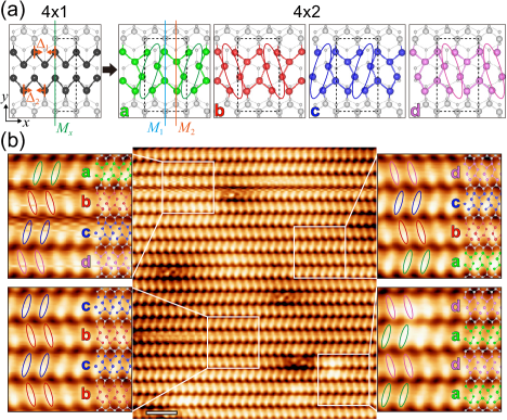
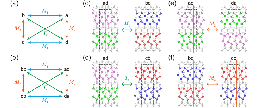
Self-assembled In nanowires on Si(111) consist of two In atomic zigzag subchains in the direction [Fig. 1(a)], which are stitched with adjacent Si chains Bunk et al. (1999); González et al. (2006); Wippermann and Schmidt (2010). Upon cooling, two In atomic subchains undergo a structural transition from to through the periodicity-doubling dimerization [ in Fig. 1(a)] along a wire. The two-way dimerization degree of freedom along both In atomic subchains spontaneously breaks the mirror symmetry of the structure Speiser et al. (2016). This broken symmetry leads to a unique CDW quartet , which consists of four symmetrically distinct CDW ground states as shown in Fig. 1(a). Each CDW ground state is chiral as it cannot be superposed onto its mirror image by any combination of rigid rotations and translations. In the CDW quartet, one can further classify chiral or achiral partners depending on their symmetry relations. For instance, is a chiral partner (mirror image) of and related by mirror operators and , respectively [Fig. 1(a)]. In contrast, () and () are achiral partners to each other since they are superposed by a half-translation operator [see also Fig. S1(a) in the Supplemental Material Sup ].
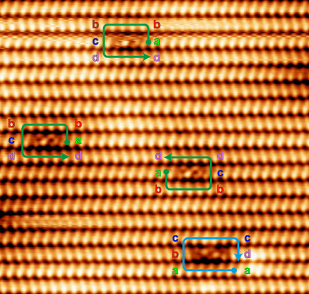
Interestingly, interwire coupling in this system forces the CDW quartet to exhibit unusual 2D ordering behavior perpendicular to the wires. As shown in Fig. 1(b), each atomic wire is alternatively stacked with its chiral partners along the axis Yeom et al. (1999). Such a local chiral order between two chiral partners is referred to as structures in previous works. With no preference for neighboring chiral partners, symmetrically inequivalent orders are apparently intermixed as witnessed by Fig. 1(b), giving rise to diffraction streaks in the low-energy electron-diffraction measurements Hatta et al. (2011). However, with careful examination of our low-temperature STM images, we found that there coexist dominant 2D chiral stacking orders among building blocks [see the insets of Fig. 1(b)]. Such exotic chiral stacking orders perpendicular to the wires are unexpected and unexplored by previous works.
| 84.2 | 4.3 | 106.5 | 0.0 | |
| 4.3 | 84.2 | 0.0 | 106.5 | |
| 106.5 | 0.0 | 84.2 | 4.3 | |
| 0.0 | 106.5 | 4.3 | 84.2 |
To find the lowest energy configuration of , we first calculate all possible structures constructed from a degenerate CDW quartet (Table I). We perceive that only four configurations represented by , , , and are symmetrically distinct not . Other possible configurations are obtained from these four structures by applying appropriate operators such as mirror or half-translation (see Fig. S1 in the Supplemental Material Sup ). As shown in Table I, is the ground state stabilized over , , and by 84.2, 4.3, and 106.5 meV per unit cell, respectively. Note that the and structures stacked by chiral partners are more stable than and stacked by achiral partners, consistent with the experimental observation in Fig. 1(b).
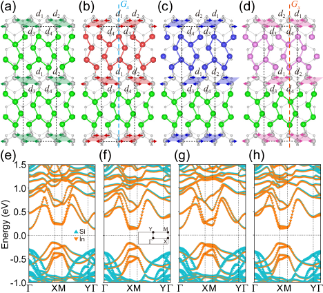
To understand the mechanism for the preference of chiral partners, we compare calculated geometries and band structures for , , , and structures (Fig. 2). Compared to an ideal structure, each structure has different dimerization patterns of Si zigzag chains [see arrows in Figs. 2(a)–2(d) and Table II]. These dimerized Si zigzag chains mainly determine the energetics in Table I. Larger Si dimerization ( and , where is an interatomic distance between Si atoms in the Si zigzag chains) leads to larger electronic energy gain; thus, , , and structures are more stable than structure. However, since the cost in lattice energy is proportional to , both larger dimerizations of a single Si zigzag chain () lead to higher energy than the case of one smaller and one larger dimerization ( and ). This finding strongly supports the alternating CDW orientations (either or ) perpendicular to the wire due to the interwire coupling. Moreover, we notice that the larger Si dimerizations are differently located in and : the larger Si dimerization () for () occurs right above the hollow (bonding) site of the Si substrate. Such a subtle difference induces the sublattice symmetry breaking, leading to the small energy difference (Table I) between the otherwise degenerate and structures. In this sense, the configuration is a true ground state having periodicity together with other symmetrically equivalent structures (, , and ), as observed in Fig. 1(b). It is noteworthy that the previous DFT studies González et al. (2009); Wippermann and Schmidt (2010); Kim and Cho (2013); Kim et al. (2015) overlooked the difference between and structures: and were used without distinction for describing experimentally observed structures. Here we clarify the ground state and present the microscopic mechanism for considerable interwire coupling in the In/Si(111) system.
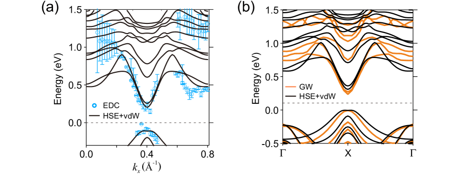
Figures 2(e)–2(h) display the calculated atom-projected band structures for , , , and configurations. They all show insulating electronic structures with the surface states composed of the hybridization between Si and In orbitals. Along the and lines, the band dispersions are not flat, which indicates that there is substantial interwire coupling in the structures. Unfavorable and structures have conduction band minima at the point, which disagrees with the observed insulating electronic structure showing conduction band minima at the point by time- and angle-resolved photoemission spectroscopy (trARPES) Nicholson et al. (2018, 2019). For and , where the overall band structures of two configurations are nearly the same, there are twofold degeneracies along the line due to the glide mirror and time-reversal symmetries: Kramers-like degeneracy protected by combined antiunitary operator along the -invariant line where in our spinless system Takahashi et al. (2017). It is noteworthy that the band structure of the configuration calculated by HSE+vdW is remarkably consistent with the trARPES experiment and is improved over previous GW calculation (see Fig. S2 in the Supplemental Material Sup ).
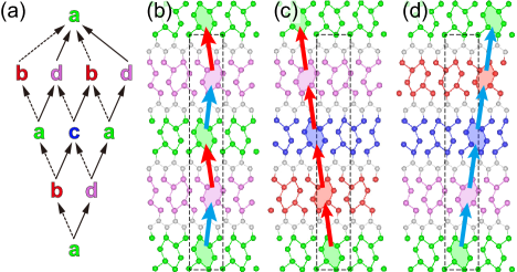
Next, we consider a longer periodicity of stacking along the axis. To explain the observed stacking periodicity in Fig. 1(b), we investigate the possible ground states based on Table I; we present a stacking sequence diagram made out of energetically favorable building blocks ( and ) as well as their symmetric equivalence (, , ; , , ) [Fig. 3(a)]. Note that, since these building blocks should be composed of chiral partners, odd-periodicity stacking such as an () structure, which inevitably involves energetically unfavorable stacking by achiral partners ( or ), is energetically not allowed. Thus, the stacking is a minimal periodicity after the periodicity.
Surprisingly, our DFT calculations show that two configurations, and , are energetically degenerate with the configuration (within meV per unit cell), which nicely explains the intermixed ordering patterns in the experimental data [Figs. 1(b) and 3(b)–3(d); see also Fig. S3 in the Supplemental Material Sup ]. To visualize the chirality of the chiral ordering between two In atomic nanowires, we introduce two different phase-shift vectors along the direction as indicated by red and blue arrows in Figs. 3(b)–3(d). Using the phase-shift vectors, 2D stacking orders of the degenerate , , and configurations can be geometrically distinguished. In Fig. 3(b), the two phase-shift vectors of the structure appear alternatively along the direction, implying nonchiral stacking order. On the other hand, the () structure shows only the left- (right-) moving phase-shift vectors along the direction, indicating its left-chiral (right-chiral) stacking order.
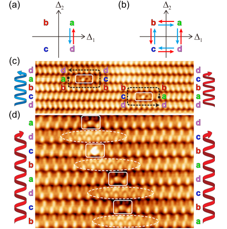
To understand topological meaning of chiral stacking orders, we characterize degenerate , , and structures with their chiral winding numbers, which are defined as the total number of turns around the gap closing point () in the order-parameter space (). When counting a chiral winding number, one counterclockwise (clockwise) turn corresponds to (). As shown in Figs. 4(a) and 4(b), all three structures uniquely show different chiral winding numbers: , , . It is noteworthy that there is a straightforward one-to-one mapping of the chiral winding numbers onto the overall phase-shift vectors described in Fig. 3.
Additionally, we discover chiral vortices and chiral domain walls that interpolate two distinct chiral stacking orders. Chiral vortices exist between two chiral stacking orders with different nonzero chiral winding numbers [Fig. 4(c)]. The vorticity of these chiral vortices is defined by counting nearby CDW ground states from , , to (see Fig. S4 in the Supplemental Material Sup ). A vortex (antivortex) shows a counterclockwise (clockwise) sequence as indicated by the dashed arrows in Fig. 4(c). In contrast to a chiral vortex, a chiral domain wall, consisting of topological solitons and In-adatom defects Song et al. (2019); Lee et al. (2019), bridges two chiral stacking orders with the same chiral winding number [Fig. 4(d)]. These observations strongly suggest that these chiral stacking orders exhibit domain topology, which is found in 2D topological systems Huang and Cheong (2017).
As witnessed in many materials, new functionalities can be obtained by engineering chiral-ordered structures using vortices or domain walls Huang and Cheong (2017). Since In nanowires show three distinct 2D chiral stacking orders, one can expect a new functionality such as circular dichroism, which shows the differential absorption of left- and right-circularly polarized light Berova et al. (2000). Further study is needed to see whether one can observe and/or control the probable circular dichroism from chiral stacking orders. For example, one may use scanning tunneling luminescence Berndt et al. (1991); Nazin et al. (2003); Kuhnke et al. (2017), which can not only measure optical response from nanometer-scale chiral stacking orders beyond diffraction limit but may also control chiral stacking orders by manipulating In adatoms with a scanning tip.
In summary, we found the 2D chiral stacking orders in arrays of quasi-1D CDW ground states using STM and DFT calculations. We experimentally observed three distinct chiral stacking orders among four CDW ground states: right-, left-, and nonchiral stacking orders. Based on the extensive DFT calculation with symmetry and topology analysis, we found that the dimerized Si zigzag chain captures the essential physics for the emergence of the chiral stacking orders and classified the three chiral stacking orders by the topological chiral winding numbers. Furthermore, topological solitons and defects play important roles as chiral domain walls and vortices between distinct 2D chiral stacking orders. Our findings open a research platform to explore the chirality in 1D charge-ordered systems, which may provide new functionalities such as circular dichroism.
Acknowledgements.
This work was supported by the National Research Foundation of Korea (NRF) funded by the Ministry of Science and ICT, South Korea (Grants No. NRF-2018R1C1B6007607, No. NRF-2018R1A5A6075964, and No. 2016K1A4A4A01922028). S.-W.K. and S.C. were supported by the research fund of Hanyang University (HY-2017). S.-W.K., H.-J.K., and S.C. acknowledge support from POSCO Science Fellowship of POSCO TJ Park Foundation. H.-J.K. acknowledges financial support from the AIDAS project of the Forschungszentrum Jülich and CEA. We thank the Korea Institute for Advanced Study for providing computing resources (KIAS Center for Advanced Computation Linux Cluster System) for this work.References
- Hyde et al. (1996) S. Hyde, Z. Blum, T. Landh, S. Lidin, B. W. Ninham, S. Andersson, and K. Larsson, The Language of Shape: The Role of Curvature in Condensed Matter: Physics, Chemistry and Biology (Elsevier, New York, 1996).
- Braun (2012) H.-B. Braun, Adv. Phys. 61, 1 (2012).
- Nagaosa and Tokura (2013) N. Nagaosa and Y. Tokura, Nat. Nanotechnol. 8, 899 (2013).
- Armitage et al. (2018) N. P. Armitage, E. J. Mele, and A. Vishwanath, Rev. Mod. Phys. 90, 015001 (2018).
- Ishioka et al. (2010) J. Ishioka, Y. H. Liu, K. Shimatake, T. Kurosawa, K. Ichimura, Y. Toda, M. Oda, and S. Tanda, Phys. Rev. Lett. 105, 176401 (2010).
- Castellan et al. (2013) J.-P. Castellan, S. Rosenkranz, R. Osborn, Q. Li, K. E. Gray, X. Luo, U. Welp, G. Karapetrov, J. P. C. Ruff, and J. van Wezel, Phys. Rev. Lett. 110, 196404 (2013).
- Xu et al. (2020) S.-Y. Xu, Q. Ma, Y. Gao, A. Kogar, A. Zong, A. M. Mier Valdivia, T. H. Dinh, S.-M. Huang, B. Singh, C.-H. Hsu, T.-R. Chang, J. P. C. Ruff, K. Watanabe, T. Taniguchi, H. Lin, G. Karapetrov, D. Xiao, P. Jarillo-Herrero, and N. Gedik, Nature (London) 578, 545 (2020).
- Hildebrand et al. (2018) B. Hildebrand, T. Jaouen, M.-L. Mottas, G. Monney, C. Barreteau, E. Giannini, D. R. Bowler, and P. Aebi, Phys. Rev. Lett. 120, 136404 (2018).
- Kim and Yeom (2012) T.-H. Kim and H. W. Yeom, Phys. Rev. Lett. 109, 246802 (2012).
- Cheon et al. (2015) S. Cheon, T.-H. Kim, S.-H. Lee, and H. W. Yeom, Science 350, 182 (2015).
- Kim et al. (2017) T.-H. Kim, S. Cheon, and H. W. Yeom, Nat. Phys. 13, 444 (2017).
- Yeom et al. (1999) H. W. Yeom, S. Takeda, E. Rotenberg, I. Matsuda, K. Horikoshi, J. Schaefer, C. M. Lee, S. D. Kevan, T. Ohta, T. Nagao, and S. Hasegawa, Phys. Rev. Lett. 82, 4898 (1999).
- Heyd et al. (2003) J. Heyd, G. E. Scuseria, and M. Ernzerhof, J. Chem. Phys. 118, 8207 (2003).
- Krukau et al. (2006) A. V. Krukau, O. A. Vydrov, A. F. Izmaylov, and G. E. Scuseria, J. Chem. Phys. 125, 224106 (2006).
- Tkatchenko and Scheffler (2009) A. Tkatchenko and M. Scheffler, Phys. Rev. Lett. 102, 073005 (2009).
- Zhang et al. (2011) G.-X. Zhang, A. Tkatchenko, J. Paier, H. Appel, and M. Scheffler, Phys. Rev. Lett. 107, 245501 (2011).
- Blum et al. (2009) V. Blum, R. Gehrke, F. Hanke, P. Havu, V. Havu, X. Ren, K. Reuter, and M. Scheffler, Comput. Phys. Commun. 180, 2175 (2009).
- Kim and Cho (2013) H.-J. Kim and J.-H. Cho, Phys. Rev. Lett. 110, 116801 (2013).
- Zhang et al. (2014) H. Zhang, F. Ming, H.-J. Kim, H. Zhu, Q. Zhang, H. H. Weitering, X. Xiao, C. Zeng, J.-H. Cho, and Z. Zhang, Phys. Rev. Lett. 113, 196802 (2014).
- Kim et al. (2015) S.-W. Kim, H.-J. Kim, F. Ming, Y. Jia, C. Zeng, J.-H. Cho, and Z. Zhang, Phys. Rev. B 91, 174434 (2015).
- Kim and Cho (2016) S.-W. Kim and J.-H. Cho, Phys. Rev. B 93, 241408(R) (2016).
- Tanikawa et al. (2004) T. Tanikawa, I. Matsuda, T. Kanagawa, and S. Hasegawa, Phys. Rev. Lett. 93, 016801 (2004).
- González et al. (2009) C. González, J. Guo, J. Ortega, F. Flores, and H. H. Weitering, Phys. Rev. Lett. 102, 115501 (2009).
- Bunk et al. (1999) O. Bunk, G. Falkenberg, J. H. Zeysing, L. Lottermoser, R. L. Johnson, M. Nielsen, F. Berg-Rasmussen, J. Baker, and R. Feidenhans’l, Phys. Rev. B 59, 12228 (1999).
- González et al. (2006) C. González, F. Flores, and J. Ortega, Phys. Rev. Lett. 96, 136101 (2006).
- Wippermann and Schmidt (2010) S. Wippermann and W. G. Schmidt, Phys. Rev. Lett. 105, 126102 (2010).
- Speiser et al. (2016) E. Speiser, N. Esser, S. Wippermann, and W. G. Schmidt, Phys. Rev. B 94, 075417 (2016).
- (28) See Supplemental Material at [URL will be inserted by publisher] for additional data and interpretations.
- Hatta et al. (2011) S. Hatta, Y. Ohtsubo, T. Aruga, S. Miyamoto, H. Okuyama, H. Tajiri, and O. Sakata, Phys. Rev. B 84, 245321 (2011).
- (30) Note that the structure with a rectangular unit cell (Fig. 2) can be considered as the structure with a parallelogram unit cell.
- Nicholson et al. (2018) C. W. Nicholson, A. Lücke, W. G. Schmidt, M. Puppin, L. Rettig, R. Ernstorfer, and M. Wolf, Science 362, 821 (2018).
- Nicholson et al. (2019) C. W. Nicholson, M. Puppin, A. Lücke, U. Gerstmann, M. Krenz, W. G. Schmidt, L. Rettig, R. Ernstorfer, and M. Wolf, Phys. Rev. B 99, 155107 (2019).
- Takahashi et al. (2017) R. Takahashi, M. Hirayama, and S. Murakami, Phys. Rev. B 96, 155206 (2017).
- Song et al. (2019) S. K. Song, A. Samad, S. Wippermann, and H. W. Yeom, Nano Lett. 19, 5769 (2019).
- Lee et al. (2019) G. Lee, H. Shim, J.-M. Hyun, and H. Kim, Phys. Rev. Lett. 122, 016102 (2019).
- Huang and Cheong (2017) F.-T. Huang and S.-W. Cheong, Nat. Rev. Mater. 2, 17004 (2017).
- Berova et al. (2000) N. Berova, K. Nakanishi, and R. W. Woody, Circular Dichroism: Principles and Applications, 2nd ed. (Wiley-VCH, New York, 2000).
- Berndt et al. (1991) R. Berndt, J. K. Gimzewski, and P. Johansson, Phys. Rev. Lett. 67, 3796 (1991).
- Nazin et al. (2003) G. V. Nazin, X. H. Qiu, and W. Ho, Phys. Rev. Lett. 90, 216110 (2003).
- Kuhnke et al. (2017) K. Kuhnke, C. Große, P. Merino, and K. Kern, Chem. Rev. 117, 5174 (2017).
Supplemental Material: Two-dimensional chiral stacking orders in quasi-one-dimensional charge density waves