Valley-dependent properties of monolayer MoSi2N4, WSi2N4 and MoSi2As4
Abstract
In a recent work, new two-dimensional materials, the monolayer MoSi2N4 and WSi2N4, have been successfully synthesized in experiment, and several other monolayer materials with the similar structure, such as MoSi2As4, have been predicted [Science 369, 670-674 (2020)]. Here, based on first-principles calculations and theoretical analysis, we investigate the electronic and optical properties of monolayer MoSi2N4, WSi2N4 and MoSi2As4. We show that these materials are semiconductors, with a pair of Dirac-type valleys located at the corners of the hexagonal Brillouin zone. Due to the broken inversion symmetry and the effect of spin-orbit coupling, the valley fermions manifest spin-valley coupling, valley-contrasting Berry curvature, and valley-selective optical circular dichroism. We also construct the low-energy effective model for the valleys, calculate the spin Hall conductivity and the permittivity, and investigate the strain effect on the band structure. Our result reveals interesting valley physics in monolayer MoSi2N4, WSi2N4 and MoSi2As4, suggesting their great potential for valleytronics and spintronics applications.
I Introduction
Since the discovery of graphene Novoselov et al. (2004, 2005a); Zhang et al. (2005), two-dimensional (2D) materials have been receiving tremendous attention, because of their extraordinary properties and promising applications Novoselov et al. (2005b); Bhimanapati et al. (2015); Das et al. (2015); Tan et al. (2017). With the rapid advance of experimental technique, many new 2D materials beyond graphene have been realized, such as silicene and germanene Cahangirov et al. (2009); Liu et al. (2011), 2D hexagonal boron nitride Lin et al. (2010); Weng et al. (2016); Li and Chen (2016), 2D transition metal dichalcogenides Mak et al. (2010); Chhowalla et al. (2013); Huang et al. (2013); Tan and Zhang (2015); Lv et al. (2015), black phosphorene Li et al. (2014a); Liu et al. (2015); Eswaraiah et al. (2016), MXenes Naguib et al. (2011, 2012, 2014), and so on.
The progress in 2D materials also generates impetus for many other fields, such as the field of valleytronics Schaibley et al. (2016); Vitale et al. (2018). As an emerging degree of freedom, valley refers to the presence of multiple energy extremal points in the Brillouin zone (BZ) for low-energy carriers in a semiconductor. Analogous to charge and spin, the valley degree of freedom can be exploited for information encoding and processing, leading to the concept of valleytronics Gunawan et al. (2006); Rycerz et al. (2007); Xiao et al. (2007); Yao et al. (2008); Gunlycke and White (2011); Xiao et al. (2012); Zhu et al. (2012); Cai et al. (2013); Jiang et al. (2013); Xu et al. (2014); Pan et al. (2015a, b); Sui et al. (2015); Cheng et al. (2018); Yu et al. (2020). Although the possibility to control valley polarization had been demonstrated in certain 3D materials Zhu et al. (2012), it was with the advent of 2D materials that the field truly flourished. In 2D materials such as graphene and MoS2-family monolayers, there are a single pair of Dirac-type valleys, forming a binary degree of freedom. Particularly, Xiao et al. Xiao et al. (2007) and Yao et al. Yao et al. (2008) proposed that such valleys possess contrasting geometric properties like Berry curvature and orbital magnetic moment, which generates interesting effects such as the valley Hall effect and the optical circular dichroism. The orbital magnetic moment also allows a control of valley polarization via applied magnetic field Cai et al. (2013). These proposals have been successfully demonstrated in experiments Mak et al. (2012); Zeng et al. (2012); Cao et al. (2012); Li et al. (2014b); Ju et al. (2015); Aivazian et al. (2015); Srivastava et al. (2015); MacNeill et al. (2015); Jiang et al. (2017); Li et al. (2018).
Very recently, new 2D materials of monolayer MoSi2N4 and WSi2N4 were synthesized in experiment Hong et al. (2020). It was found that they are semiconductors with high strength and excellent ambient stability. Based on calculations, a family of 2D materials with the similar structure, such as monolayer MoSi2As4, have also been predicted Hong et al. (2020); Wang et al. (2020). Motivated by the discovery of these new materials, in this work, based on first-principles calculations and theoretical modeling, we investigate the electronic and optical properties of monolayer MoSi2N4, WSi2N4 and MoSi2As4, focusing on the valleytronic aspects. We show that in terms of valley structures, these materials are very similar to the MoS2-family monolayers. They have a pair of Dirac-type valleys located at the corners of the hexagonal BZ, connected by the time reversal symmetry. With the broken inversion symmetry and sizable spin-orbit coupling (SOC), the two valleys exhibit contrasting features in spin splitting, Berry curvature, and optical circular dichroism. This means the valley polarization in these materials can also be effectively controlled by transport, optical, and magnetic means. In addition, we show that the lattice strain can be utilized to tune the band structures, and may drive transitions between direct and indirect band gaps in these materials. Given that these 2D materials have gap sizes complementary to the 2D MoS2-family materials, our results here suggest their great potential for valleytronic and spintronic applications.
II Computation METHODS
Our first-principles calculations were based on the density functional theory (DFT), using the projector augmented wave method as implemented in the Vienna ab initio simulation package Kresse and Hafner (1994); Kresse and Furthmüller (1996); Blöchl (1994). The generalized gradient approximation with the Perdew-Burke-Ernzerhof (PBE) Perdew et al. (1996) realization was adopted for the exchange-correlation functional. The band structure result was further checked by using the more accurate Heyd-Scuseria-Ernzerhof hybrid functional method (HSE06) Heyd et al. (2003) (see Appendix A). The cutoff energy was set as 500 eV. The energy and force convergence criteria were set to be eV and eV/Å, respectively. The BZ was sampled with a -centered mesh of size . A vacuum layer with a thickness of 20 Å was taken to avoid artificial interactions between periodic images. The PyProcar code Herath et al. (2020) was used to plot the band structure with the spin polarization. We construct Wannier functions by projecting the Bloch states onto atomic-like trial orbitals without an iterative procedure Marzari and Vanderbilt (1997); Souza et al. (2001); Mostofi et al. (2008). In the calculation of the intrinsic spin Hall conductivity [Eq. (6)], a dense -point mesh of size was adopted. And for the permittivity calculation, a -point mesh with size was used. The permittivities are suitably renormalized to exclude the vacuum region by using the experimental value 10.7 Å as the effective thickness Hong et al. (2020).
III electronic band and valley structures
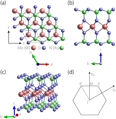
The monolayer MoSi2N4 and WSi2N4 have been experimentally realized by the chemical vapor deposition (CVD) method Hong et al. (2020). These two materials and MoSi2As4 share the same type of hexagonal lattice structure with space group (No. ). As shown in Fig. 1(a)-1(c), the structure is built up by septuple atomic layers in the sequence of N(As)-Si-N(As)-Mo(W)-N(As)-Si-N(As). It is important to note that the structure breaks the inversion symmetry, but preserves a horizontal mirror corresponding to the plane of the Mo (W) layer. From our first-principles calculation, the fully optimized lattice parameters for monolayer MoSi2N4, WSi2N4, and MoSi2As4 are Å, Å, and Å, respectively. These parameters agree well with the previously reported values Hong et al. (2020).
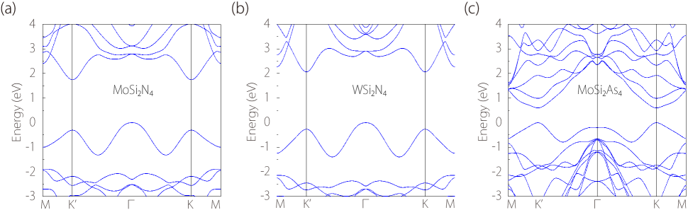
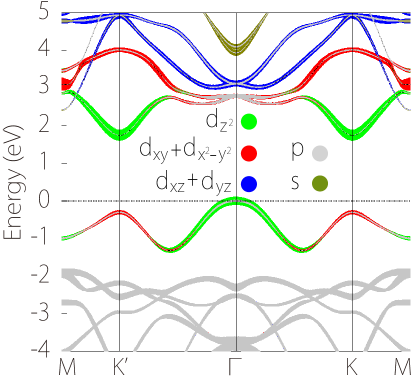
We then investigate the electronic band structures of these three materials. We first calculate the band structures in the absence of SOC. The obtained results are plotted in Fig. 2. One observes that MoSi2N4 and WSi2N4 are indirect band-gap semiconductors with the conduction-band minimum (CBM) at / and valence-band maximum (VBM) at . Here, and are the two inequivalent corners of the hexagonal BZ [see Fig. 1(d)]. In contrast, MoSi2As4 is a direct band-gap semiconductor with both CBM and VBM at /. To understand the composition of the low-energy states, we project the states to atomic orbitals of the constituent atoms. The result for MoSi2N4 is shown in Fig. 3. The important observation is that the states near the band edges are dominated by the Mo- orbitals. More specifically, the states around CBM at / are dominated by the Mo orbital. As for the highest valence band, the states around are also dominated by the Mo orbital, but the states around / are dominated by the Mo and orbitals. This orbital character is also shared by the other two materials WSi2N4 and MoSi2As4.
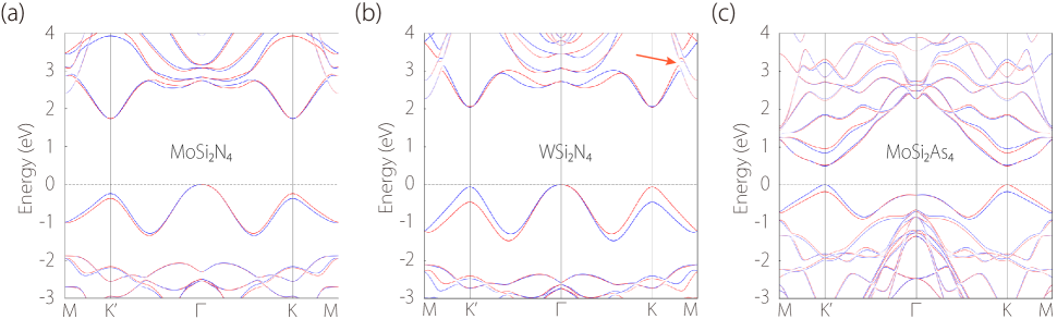
Next, we consider the band structures with SOC included, and the results are plotted in Fig. 4. One observes that MoSi2N4 and WSi2N4 are still indirect band-gap semiconductors, and MoSi2As4 still retains a direct band gap. The obtained band gap values with PBE method are listed in Table 1. We have also use the more sophisticated hybrid functional method (HSE06) Heyd et al. (2003) to check the band structure results. We find that the main band features are consistent between these two methods, except that for WSi2N4, HSE06 predicts a direct band gap with the valence state at / about 5 meV higher than that of the point. The band gap values from HSE06 approach are also listed in Table 1 for comparison. The corrections of HSE06 on PBE band gaps are 0.556 eV, 0.564 eV, and 0.191 eV for monolayer MoSi2N4, WSi2N4, and MoSi2As4, respectively. These values are lower than the corresponding corrections for some bulk semiconductors like GaN, Si, and GaAs Heyd et al. (2005), but they are comparable to those for the 2D MoS2-family materials Ramasubramaniam (2012).
Compared with Fig. 2, one observes that the main effect of SOC in Fig. 4 is to cause a spin splitting of the original bands. Here, we use the red/blue color to indicate the spin polarization of the band eigenstate . From the symmetry perspective, the spin splitting is a direct consequence of the inversion symmetry breaking, which lifts the spin degeneracy at each generic point. Moreover, due to the existence of the horizontal mirror which operates on spin as , the band eigenstates must also be eigenstates of the operator, i.e., they are fully spin-polarized in the out-of-plane direction. Lastly, the time reversal symmetry is preserved in the system, so that the spin polarizations at and are opposite, as the two points are connected by the operation. This is particularly evident when looking at the highest valence band in Fig. 4.
From the band structures in Fig. 4, another important observation is that there exists a valley degree of freedom. All three materials have conduction band valleys at and . For monolayer MoSi2As4, its valence band also has valleys at and , whereas for the other two materials, although the VBM occurs at , the / valleys are still well defined and not far in energy. As we have mentioned, and points are connected by the time reversal operation, so any property that is odd under will have opposite values between the and valleys. The spin polarization we just analyzed is one such example. In the following, we shall examine other properties, and these will be useful for controlling the valley degree of freedom, as has been originally proposed in Refs. Xiao et al. (2007); Yao et al. (2008); Cai et al. (2013). Note that the exact gap values will not affect the main features of the valley properties, so in the following, we shall base our discussion mostly on the PBE band structures.
| Method | ||||
|---|---|---|---|---|
| MoSi2N4 | PBE | 1.742 | 1.976 | 0.129 |
| HSE06 | 2.298 | 2.442 | 0.172 | |
| WSi2N4 | PBE | 2.044 | 2.087 | 0.404 |
| HSE06 | 2.608 | 2.608 | 0.513 | |
| MoSi2As4 | PBE | 0.500 | 0.500 | 0.180 |
| HSE06 | 0.691 | 0.691 | 0.284 |
IV effective model
To better understand the valley properties, we shall first construct an effective model which describes the valley structures at and points. As analyzed in Sec. III, the conduction band at / is dominated by the orbital, whereas the valence band at / is dominated by the and orbitals. This feature is similar to the case in monolayer MoS2. At and , the little group is which may be generated by the symmetry elements and . By choosing the two orbital basis and , where is the valley index corresponding to /, the effective model at / in the absence of SOC can be obtained as (expanded to linear order in )
| (1) |
where is measured from /, ’s are the Pauli matrices denoting the two-orbital degree of freedom, and are real valued model parameters.
Then, SOC is taken into account as a perturbation to the Hamiltonian in Eq. (1). Approximating the SOC term as an intra-atomic contribution and keeping only the leading order (in ) term, we obtain the effective model in the presence of SOC as
| (2) |
where is the Pauli matrix for spin and represents the effective SOC strength. Compared with the band structures in Fig. 4, one observes that the SOC term in (2) captures the key feature of spin splitting at /: the splitting is pronounced in the valence band (with a value of ), whereas it is very small for the conduction band. In addition, the SOC term shows that the spins are fully polarization in the out-of-plane direction due to the symmetry, as we mentioned before. We have used this model to fit the DFT band structures. The extracted model parameters are listed in Table 2.
The effective model (2) is diagonal in the real spin. For each spin channel , the model takes a form of a gapped Dirac model. This demonstrates that the valleys at and here are Dirac-type valleys Yang (2016). One can observe that model (2) has essentially the same form as that for the monolayer MoS2-family materials Xiao et al. (2012). This is because both classes of materials have similar low-energy band structures at /, and they possess the same symmetry group. Thus, regarding the valley structure, these three materials are very similar to the monolayer MoS2-family materials. Nevertheless, there are also differences between them. For example, the band gap in MoSi2As4 is smaller than the MoS2-family materials (typically 1.5 to 2 eV), and the gaps in MoSi2N4 and WSi2N4 are larger, so they offer an energy coverage complementary to the MoS2-family materials.
| Method | ||||
|---|---|---|---|---|
| MoSi2N4 | PBE | 4.021 | 2.041 | 0.065 |
| HSE06 | 5.080 | 2.528 | 0.086 | |
| WSi2N4 | PBE | 4.756 | 2.289 | 0.202 |
| HSE06 | 5.876 | 2.865 | 0.257 | |
| MoSi2As4 | PBE | 2.244 | 0.590 | 0.090 |
| HSE06 | 3.102 | 0.833 | 0.142 |
V Valley-contrasting Berry curvature and circular dichroism
Dirac-type valleys possess interesting physical properties such as Berry curvature and optical circular dichroism. It is important to note that these properties are odd under , so they will take opposite values for the two valleys and .
Let’s first consider the Berry curvature. For 2D systems, it only has a component, which behaves as a pseudoscalar. For a state , its Berry curvature can be calculated by
| (3) |
where the ’s are the velocity operators, and is the energy of the state . By using the effective model (2), one finds that the Berry curvature for the two conduction bands (with opposite ) at / valley is given by
| (4) |
where . And for the two spin-split valence bands at /, we have
| (5) |
It is clearly from Eq. (4) that the two valleys have nonzero and opposite Berry curvatures. The magnitude of the Berry curvature is peaked at the valley center .
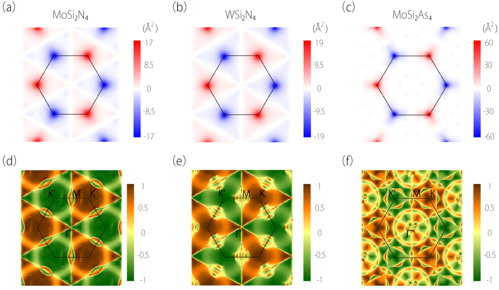
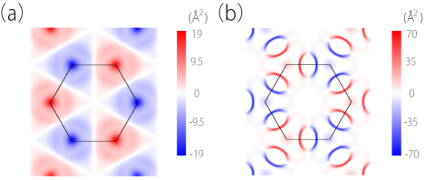
In Fig. 5 and Fig. 6, we have shown the Berry curvature distribution obtained from DFT calculations, which go beyond the effective model. In Fig. 5, we plot the total Berry curvature for all the valence bands for the three materials. One clearly observes that the distribution is peaked and takes opposite values at and valleys. In Fig. 6(b) [Fig. 6(a)], we also plot the combined Berry curvature for the two conduction (valence) bands closest to the band gap for monolayer WSi2N4 (results for the other two are similar). The valley-contrasting character is also faithfully reproduced. We note that in Ref. Wang et al. (2020), Berry curvature distribution with similar valley features was also found in monolayer . In Fig. 6(b), one observes there are additional sharp features between / and . These are at higher energy and due to the band near-degeneracies as marked in Fig. 4(b).
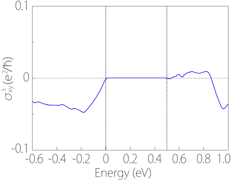
Such nonzero Berry curvature is the key ingredient for the anomalous Hall transport, which means a longitudinal (in-plane) field will deflect carriers in transverse directions without applied magnetic field. This is most readily understood in the semiclassical formalism Xiao et al. (2010), where the Berry curvature directly enters into the equations of motion and generates a so-called anomalous velocity term . For our current systems, there is no net charge current at linear order because the symmetry is preserved. However, there could exist valley and spin Hall effect. The valley Hall effect occurs in these materials immediately after electron doping. As for hole doping, in MoSi2N4 and WSi2N4, one has to reach a doping level with / valleys occupied to observe the effect. The case with hole doping in MoSi2As4 could be more interesting. There, the VBM occurs at and , and the valleys are spin polarized. The valley Hall effect is therefore associated with a pronounced spin Hall effect. We have evaluated the intrinsic spin Hall conductivity for the doped monolayer MoSi2As4, defined by
| (6) |
where is the equilibrium distribution function for the doped carriers, is the spin polarization of the state , and we have included an extra factor of in the definition such that the magnitude of can be better compared with charge conductivities. The result obtained from the DFT calculation is plotted in Fig. 7. One observes that takes a negative value for hole doping and switches sign for electron doping (and again there is a sign change around 0.8 eV). The magnitude of the spin Hall conductivity () under hole doping is comparable to that of MoS2-family materials Feng et al. (2012). We have estimated that to achieve the peak magnitude in Fig. 7 (at about eV), the hole doping concentration is around , which can be achieved by the current experimental technique Efetov and Kim (2010); Ye et al. (2011). The Hall effect will results in both valley and spin polarizations at the edges along the transverse direction, which can be respectively detected by the optical circular dichroism and the magneto-optical Kerr effect.
The nonzero Berry curvature indicates the Dirac-type valleys have a sense of chirality, which can manifest in the effect of optical circular dichroism Yao et al. (2008). It has been shown that for a general two-band system, the degree of circular polarization is proportional to the Berry curvature Liu et al. (2018). For our current systems, at each valley there are four low energy bands. As optical transitions are vertical and preserve the spin, they can only happen between a pair of bands belonging to the same spin channel. Hence, one can consider the two spin channels separately.
The circular polarization for optical transition between a pair of states is defined by
| (7) |
where is the optical transition matrix element for incident light with circular polarizations. As , and ( is the free electron mass), the circular polarization can be readily evaluated in the effective model or by DFT calculations.
Consider the transition from the topmost valence band (which has a definite spin polarization) to the conduction band at / valleys. Using the effective model in Eq. (2), we find that the corresponding -resolved circular polarization is given by
| (8) |
At the valley center , we have , indicating that the transition at the valley center is exclusively coupled to a specific circular polarization.
The corresponding results obtained from DFT calculations for the three materials are shown in Fig. 5(d-f). Here, the plotted is for the transitions between the highest valence band and the lowest conduction band, over the whole BZ. Note that these transitions are at different light frequencies. The lowest transition frequency occurs at the two valleys, where takes opposite signs, consistent with our analysis using the effective model.
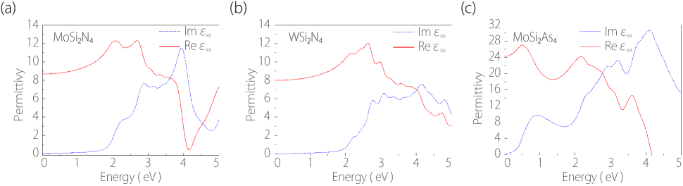
To assess the ability of optical absorption of these materials, we have also calculated their permittivity. Due to the symmetry, the permittivity tensor must be isotropic in plane. In Fig. 8, we plot the real and imaginary parts of calculated by DFT approach. The imaginary part is related to the optical absorption. The absorption edges in reflect the semiconducting band gaps. One observes that the absorption in MoSi2As4 in the visible light range is around two times stronger than in MoSi2N4 and WSi2N4. The optical absorption strength here is comparable to that of monolayer MoS2 Ahmed et al. (2015); Lahourpour et al. (2019); Ermolaev et al. (2020). The real part also manifests features of a semiconductor: it is positive in the low energy range, and below the band gap it directly determines the refractive index of the material.
VI Strain effect on band structure
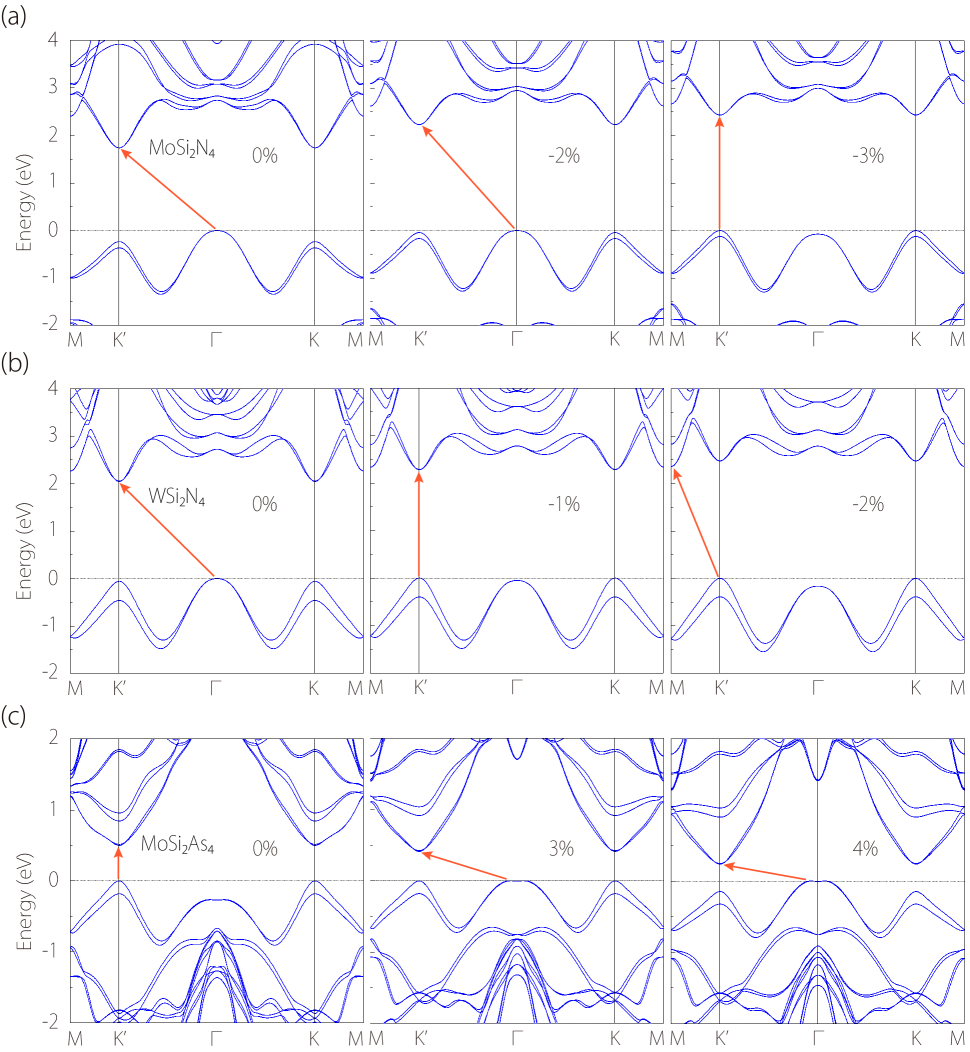
2D materials can usually sustain large lattice strains, and their properties can be effectively tuned by strain engineering. Here, we study the effect of biaxial strains on the band structures of the three materials. The most important finding is that a moderate strain () can generate a transition between direct and indirect band gaps in these materials. As shown in Fig. 9, for monolayer MoSi2N4 and WSi2N4, this transition occurs at small compressive strain of and , respectively. During the transition, the VBM switches from to / points. Interestingly, in WSi2N4, there is a second transition around , during which the VBM is unchanged (at /), but the CBM is switched from / to . Meanwhile, the transition in monolayer MoSi2As4 occurs at tensile strain around , at which the VBM changes from / to . Thus, in these materials, the low-energy band features are rather sensitive to strain. A common feature is that with increasing lattice parameter, the valence band at tends to shift up whereas the valence band at / valleys tends to move downward. This leads to the transition between indirect and direct band gaps. This feature is also verified by the more sophisticated HSE06 approach: Although the exact strain values for the transitions generally differ between different computational methods, the qualitative results still remain valid. We point out that this strain-induced transition could be useful for valley switching, i.e., the applied strain can be used to control the emergence/disappearance of the valley degree of freedom.
VII Discussion and Conclusion
In this work, we have studied the emerging valley degree of freedom in the newly synthesized 2D materials MoSi2N4 and WSi2N4, and the closely related MoSi2As4. We have shown that their valley structure is very similar to the MoS2-family materials. And we have also pointed out their noticeable differences, such as their different gap values complementary to the MoS2-family materials, indirect band gaps in some of these materials, and the strain-induced transition in the gap types. Furthermore, it should be noted as ternary compounds, there could be many more 2D materials with this type of lattice structure. Indeed, in a recent work, more than 66 2D compounds were predicted to be stable with this structure, some of which are metals and are even magnetic Hong et al. (2020); Wang et al. (2020). The analysis here may be extended to those predicted materials as well in future studies.
Besides Berry curvature, orbital magnetic moment is another important geometric property of Bloch states Xiao et al. (2010). For 2D systems, its direction is constrained to be out-of-plane, so like Berry curvature, it also behaves as a pseudoscalar. Using the effective model (2), we can find that for the conduction bands
| (9) |
where is the Bohr magneton. Hence, the orbital moments are also opposite for the two valleys, consistent with the requirement of symmetry. Different from the Berry curvature, the moments for the valence bands are given by , which do not have a flipped sign. A direct consequence of this moment is that under a magnetic field, the band structure will have an energy shift of . Here, the shift will be opposite for the two valleys. This allows the control of valley polarization by a vertical magnetic field Cai et al. (2013). Physically, this shift caused by orbital magnetic moment is closely related to the anomalous Landau levels, i.e., due to the opposite energy shift, the lowest Landau level for either conduction or valence band will have contribution from only one valley Cai et al. (2013).
In conclusion, we have revealed interesting valley physics in the newly discovered 2D materials monolayer MoSi2N4, WSi2N4, and MoSi2As4. We show that these materials are semiconductors with an emerging binary valley degree of freedom. By constructing the valley effective model, we demonstrate that these valleys are of Dirac-type, which therefore possess nontrivial valley-contrasting properties such as spin-valley coupling, Berry curvature, optical circular dichroism, and orbital magnetic moment. These properties offer great opportunities to control valleys using applied electric, magnetic, and optical fields. Furthermore, we find that the band gap type and the valleys can be effectively switched by a moderate strain. Our results thus reveal this new family of 2D materials as promising platforms for studying the valley physics and for applications in valleytronics and spintronics.
Acknowledgements.
The authors thank X. D. Zhou and D. L. Deng for valuable discussions. This work is supported by the Singapore Ministry of Education AcRF Tier 2 (Grant No. MOE2019-T2-1-001). S.G. acknowledges support from the NSF of China (Grants No.11904359). W.F. and Y.Y. acknowledge the support from the National Natural Science Foundation of China (Grants No. 11874085 and No. 11734003) and the National Key R&D Program of China (Grant No. 2016YFA0300600). The computational work for this article was performed on resources of the National Supercomputing Centre, Singapore.Appendix A Band structure results from hybrid functional approach
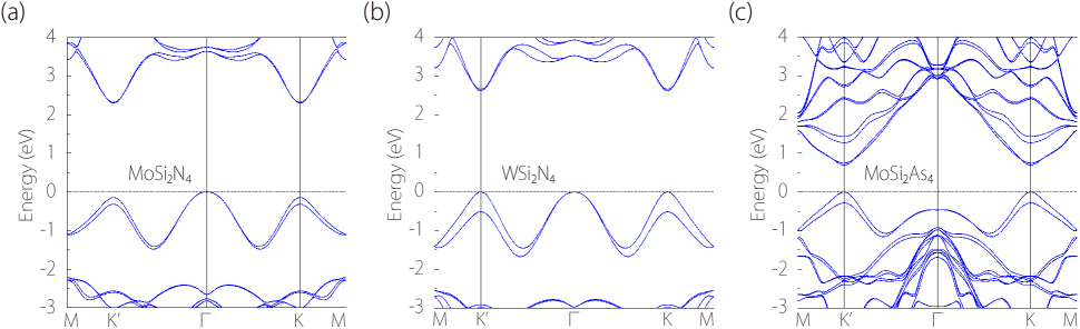
The band structures of monolayer MoSi2N4, WSi2N4 and MoSi2As4 are also checked by using the more sophisticated Heyd-Scuseria-Ernzerhof hybrid functional approach (HSE06) Heyd et al. (2003) (SOC included). The results are plotted in Fig. 10. One observes that qualitative band features are similar to the PBE results (especially for the low-energy bands at the / valleys), except that for WSi2N4, the valence band at / now becomes slightly higher than .
References
- Novoselov et al. (2004) K. S. Novoselov, A. K. Geim, S. V. Morozov, D. Jiang, Y. Zhang, S. V. Dubonos, I. V. Grigorieva, and A. A. Firsov, Science 306, 666 (2004).
- Novoselov et al. (2005a) K. S. Novoselov, A. K. Geim, S. V. Morozov, D. Jiang, M. I. Katsnelson, I. Grigorieva, S. Dubonos, and A. A. Firsov, Nature 438, 197 (2005a).
- Zhang et al. (2005) Y. Zhang, Y.-W. Tan, H. L. Stormer, and P. Kim, Nature 438, 201 (2005).
- Novoselov et al. (2005b) K. S. Novoselov, D. Jiang, F. Schedin, T. Booth, V. Khotkevich, S. Morozov, and A. K. Geim, Proc. Natl. Acad. Sci. USA 102, 10451 (2005b).
- Bhimanapati et al. (2015) G. R. Bhimanapati, Z. Lin, V. Meunier, Y. Jung, J. Cha, S. Das, D. Xiao, Y. Son, M. S. Strano, V. R. Cooper, et al., ACS nano 9, 11509 (2015).
- Das et al. (2015) S. Das, J. A. Robinson, M. Dubey, H. Terrones, and M. Terrones, Annu. Rev. Mater. Res. 45, 1 (2015).
- Tan et al. (2017) C. Tan, X. Cao, X.-J. Wu, Q. He, J. Yang, X. Zhang, J. Chen, W. Zhao, S. Han, G.-H. Nam, et al., Chem. Rev. 117, 6225 (2017).
- Cahangirov et al. (2009) S. Cahangirov, M. Topsakal, E. Aktürk, H. Şahin, and S. Ciraci, Phys. Rev. Lett. 102, 236804 (2009).
- Liu et al. (2011) C.-C. Liu, W. Feng, and Y. Yao, Phys. Rev. Lett. 107, 076802 (2011).
- Lin et al. (2010) Y. Lin, T. V. Williams, and J. W. Connell, J. Phys. Chem. Lett. 1, 277 (2010).
- Weng et al. (2016) Q. Weng, X. Wang, X. Wang, Y. Bando, and D. Golberg, Chem. Soc. Rev. 45, 3989 (2016).
- Li and Chen (2016) L. H. Li and Y. Chen, Adv. Funct. Mater. 26, 2594 (2016).
- Mak et al. (2010) K. F. Mak, C. Lee, J. Hone, J. Shan, and T. F. Heinz, Phys. Rev. Lett. 105, 136805 (2010).
- Chhowalla et al. (2013) M. Chhowalla, H. S. Shin, G. Eda, L.-J. Li, K. P. Loh, and H. Zhang, Nat. Chem. 5, 263 (2013).
- Huang et al. (2013) X. Huang, Z. Zeng, and H. Zhang, Chem. Soc. Rev. 42, 1934 (2013).
- Tan and Zhang (2015) C. Tan and H. Zhang, Chem. Soc. Rev. 44, 2713 (2015).
- Lv et al. (2015) R. Lv, J. A. Robinson, R. E. Schaak, D. Sun, Y. Sun, T. E. Mallouk, and M. Terrones, Acc. Chem. Res. 48, 56 (2015).
- Li et al. (2014a) L. Li, Y. Yu, G. J. Ye, Q. Ge, X. Ou, H. Wu, D. Feng, X. H. Chen, and Y. Zhang, Nat. Nanotechnol. 9, 372 (2014a).
- Liu et al. (2015) H. Liu, Y. Du, Y. Deng, and D. Y. Peide, Chem. Soc. Rev. 44, 2732 (2015).
- Eswaraiah et al. (2016) V. Eswaraiah, Q. Zeng, Y. Long, and Z. Liu, Small 12, 3480 (2016).
- Naguib et al. (2011) M. Naguib, M. Kurtoglu, V. Presser, J. Lu, J. Niu, M. Heon, L. Hultman, Y. Gogotsi, and M. W. Barsoum, Adv. Mater. 23, 4248 (2011).
- Naguib et al. (2012) M. Naguib, O. Mashtalir, J. Carle, V. Presser, J. Lu, L. Hultman, Y. Gogotsi, and M. W. Barsoum, ACS nano 6, 1322 (2012).
- Naguib et al. (2014) M. Naguib, V. N. Mochalin, M. W. Barsoum, and Y. Gogotsi, Adv. Mater. 26, 992 (2014).
- Schaibley et al. (2016) J. R. Schaibley, H. Yu, G. Clark, P. Rivera, J. S. Ross, K. L. Seyler, W. Yao, and X. Xu, Nat. Rev. Mater. 1, 16055 (2016).
- Vitale et al. (2018) S. A. Vitale, D. Nezich, J. O. Varghese, P. Kim, N. Gedik, P. Jarillo-Herrero, D. Xiao, and M. Rothschild, Small 14, 1801483 (2018).
- Gunawan et al. (2006) O. Gunawan, Y. Shkolnikov, K. Vakili, T. Gokmen, E. De Poortere, and M. Shayegan, Phys. Rev. Lett. 97, 186404 (2006).
- Rycerz et al. (2007) A. Rycerz, J. Tworzydło, and C. Beenakker, Nat. Phys. 3, 172 (2007).
- Xiao et al. (2007) D. Xiao, W. Yao, and Q. Niu, Phys. Rev. Lett. 99, 236809 (2007).
- Yao et al. (2008) W. Yao, D. Xiao, and Q. Niu, Phys. Rev. B 77, 235406 (2008).
- Gunlycke and White (2011) D. Gunlycke and C. T. White, Phys. Rev. Lett. 106, 136806 (2011).
- Xiao et al. (2012) D. Xiao, G.-B. Liu, W. Feng, X. Xu, and W. Yao, Phys. Rev. Lett. 108, 196802 (2012).
- Zhu et al. (2012) Z. Zhu, A. Collaudin, B. Fauqué, W. Kang, and K. Behnia, Nat. Phys. 8, 89 (2012).
- Cai et al. (2013) T. Cai, S. A. Yang, X. Li, F. Zhang, J. Shi, W. Yao, and Q. Niu, Phys. Rev. B 88, 115140 (2013).
- Jiang et al. (2013) Y. Jiang, T. Low, K. Chang, M. I. Katsnelson, and F. Guinea, Phys. Rev. Lett. 110, 046601 (2013).
- Xu et al. (2014) X. Xu, W. Yao, D. Xiao, and T. F. Heinz, Nat. Phys. 10, 343 (2014).
- Pan et al. (2015a) H. Pan, X. Li, F. Zhang, and S. A. Yang, Phys. Rev. B 92, 041404 (2015a).
- Pan et al. (2015b) H. Pan, X. Li, H. Jiang, Y. Yao, and S. A. Yang, Phys. Rev. B 91, 045404 (2015b).
- Sui et al. (2015) M. Sui, G. Chen, L. Ma, W.-Y. Shan, D. Tian, K. Watanabe, T. Taniguchi, X. Jin, W. Yao, D. Xiao, et al., Nat. Phys. 11, 1027 (2015).
- Cheng et al. (2018) S.-g. Cheng, H. Liu, H. Jiang, Q.-F. Sun, and X. Xie, Phys. Rev. Lett. 121, 156801 (2018).
- Yu et al. (2020) Z.-M. Yu, S. Guan, X.-L. Sheng, W. Gao, and S. A. Yang, Phys. Rev. Lett. 124, 037701 (2020).
- Mak et al. (2012) K. F. Mak, K. He, J. Shan, and T. F. Heinz, Nat. Nanotechnol. 7, 494 (2012).
- Zeng et al. (2012) H. Zeng, J. Dai, W. Yao, D. Xiao, and X. Cui, Nat. Nanotechnol. 7, 490 (2012).
- Cao et al. (2012) T. Cao, G. Wang, W. Han, H. Ye, C. Zhu, J. Shi, Q. Niu, P. Tan, E. Wang, B. Liu, et al., Nat. Commun. 3, 887 (2012).
- Li et al. (2014b) Y. Li, J. Ludwig, T. Low, A. Chernikov, X. Cui, G. Arefe, Y. D. Kim, A. M. Van Der Zande, A. Rigosi, H. M. Hill, et al., Phys. Rev. Lett. 113, 266804 (2014b).
- Ju et al. (2015) L. Ju, Z. Shi, N. Nair, Y. Lv, C. Jin, J. Velasco Jr, C. Ojeda-Aristizabal, H. A. Bechtel, M. C. Martin, A. Zettl, et al., Nature 520, 650 (2015).
- Aivazian et al. (2015) G. Aivazian, Z. Gong, A. M. Jones, R.-L. Chu, J. Yan, D. G. Mandrus, C. Zhang, D. Cobden, W. Yao, and X. Xu, Nat. Phys. 11, 148 (2015).
- Srivastava et al. (2015) A. Srivastava, M. Sidler, A. V. Allain, D. S. Lembke, A. Kis, and A. Imamoğlu, Nat. Phys. 11, 141 (2015).
- MacNeill et al. (2015) D. MacNeill, C. Heikes, K. F. Mak, Z. Anderson, A. Kormányos, V. Zólyomi, J. Park, and D. C. Ralph, Phys. Rev. Lett. 114, 037401 (2015).
- Jiang et al. (2017) C. Jiang, F. Liu, J. Cuadra, Z. Huang, K. Li, A. Rasmita, A. Srivastava, Z. Liu, and W.-B. Gao, Nat. Commun. 8, 802 (2017).
- Li et al. (2018) J. Li, R.-X. Zhang, Z. Yin, J. Zhang, K. Watanabe, T. Taniguchi, C. Liu, and J. Zhu, Science 362, 1149 (2018).
- Hong et al. (2020) Y.-L. Hong, Z. Liu, L. Wang, T. Zhou, W. Ma, C. Xu, S. Feng, L. Chen, M.-L. Chen, D.-M. Sun, et al., Science 369, 670 (2020).
- Wang et al. (2020) L. Wang, Y. Shi, M. Liu, Y.-L. Hong, M.-X. Chen, R. Li, Q. Gao, W. Ren, H.-M. Cheng, Y. Li, and X.-Q. Chen, arXiv:2008.02981 (2020).
- Kresse and Hafner (1994) G. Kresse and J. Hafner, Phys. Rev. B 49, 14251 (1994).
- Kresse and Furthmüller (1996) G. Kresse and J. Furthmüller, Phys. Rev. B 54, 11169 (1996).
- Blöchl (1994) P. E. Blöchl, Phys. Rev. B 50, 17953 (1994).
- Perdew et al. (1996) J. P. Perdew, K. Burke, and M. Ernzerhof, Phys. Rev. Lett. 77, 3865 (1996).
- Heyd et al. (2003) J. Heyd, G. E. Scuseria, and M. Ernzerhof, J. Chem. Phys. 118, 8207 (2003).
- Herath et al. (2020) U. Herath, P. Tavadze, X. He, E. Bousquet, S. Singh, F. Munoz, and A. H. Romero, Comput. Phys. Commun. 251, 107080 (2020).
- Marzari and Vanderbilt (1997) N. Marzari and D. Vanderbilt, Phys. Rev. B 56, 12847 (1997).
- Souza et al. (2001) I. Souza, N. Marzari, and D. Vanderbilt, Phys. Rev. B 65, 035109 (2001).
- Mostofi et al. (2008) A. A. Mostofi, J. R. Yates, Y.-S. Lee, I. Souza, D. Vanderbilt, and N. Marzari, Comput. Phys. Commun. 178, 685 (2008).
- Heyd et al. (2005) J. Heyd, J. E. Peralta, G. E. Scuseria, and R. L. Martin, J. Chem. Phys. 123, 174101 (2005).
- Ramasubramaniam (2012) A. Ramasubramaniam, Physical Review B 86, 115409 (2012).
- Yang (2016) S. A. Yang, SPIN 06, 1640003 (2016).
- Xiao et al. (2010) D. Xiao, M.-C. Chang, and Q. Niu, Rev. Mod. Phys. 82, 1959 (2010).
- Feng et al. (2012) W. Feng, Y. Yao, W. Zhu, J. Zhou, W. Yao, and D. Xiao, Phys. Rev. B 86, 165108 (2012).
- Efetov and Kim (2010) D. K. Efetov and P. Kim, Phys. Rev. Lett. 105, 256805 (2010).
- Ye et al. (2011) J. Ye, M. F. Craciun, M. Koshino, S. Russo, S. Inoue, H. Yuan, H. Shimotani, A. F. Morpurgo, and Y. Iwasa, Proc. Natl. Acad. Sci. USA 108, 13002 (2011).
- Liu et al. (2018) Y. Liu, S. A. Yang, and F. Zhang, Phys. Rev. B 97, 035153 (2018).
- Ahmed et al. (2015) T. Ahmed, N. Modine, and J.-X. Zhu, Appl. Phys. Lett. 107, 043903 (2015).
- Lahourpour et al. (2019) F. Lahourpour, A. Boochani, S. Parhizgar, and S. Elahi, J. Theor. Appl. Phys. 13, 191 (2019).
- Ermolaev et al. (2020) G. A. Ermolaev, Y. V. Stebunov, A. A. Vyshnevyy, D. E. Tatarkin, D. I. Yakubovsky, S. M. Novikov, D. G. Baranov, T. Shegai, A. Y. Nikitin, A. V. Arsenin, et al., npj 2D Mater. Appl. 4, 21 (2020).