Tuning the Ultrafast Response of Fano Resonances in Halide Perovskite Nanoparticles
Abstract
The full control of the fundamental photophysics of nanosystems at frequencies as high as few THz is key for tunable and ultrafast nano-photonic devices and metamaterials. Here we combine geometrical and ultrafast control of the optical properties of halide perovskite nanoparticles, which constitute a prominent platform for nanophotonics. The pulsed photoinjection of free carriers across the semiconducting gap leads to a sub-picosecond modification of the far-field electromagnetic properties that is fully controlled by the geometry of the system. When the nanoparticle size is tuned so as to achieve the overlap between the narrowband excitons and the geometry-controlled Mie resonances, the ultrafast modulation of the transmittivity is completely reversed with respect to what is usually observed in nanoparticles with different sizes, in bulk systems and in thin films. The interplay between chemical, geometrical and ultrafast tuning offers an additional control parameter with impact on nano-antennas and ultrafast optical switches.
Introduction
The study of light-matter interaction in halide perovskites (HPs) has revolutionized the photonics community in the last decade review10years ; Fu2019 . The wide interest on this class of materials, which comprises compounds of the form ABX3, where A stands for organic (e.g., CH3NH3=MA) or inorganic (e.g., Cs) cations, B is usually lead (Pb), and X is chosen between the halogens I, Br, or Cl, mainly stems from their outstanding optoelectronic properties, such as strong excitonic resonances at room temperature Green2014 , tunable band-gaps and emission wavelengths within the entire visible spectrum Jang2015 ; Protescu2015 ; Byun2017 , and long carrier diffusion lengths Wehrenfennig2014 ; Dong-science-2015 . These features, combined with low-cost fabrication methods, boosted the development of photovoltaic solar cells with power conversion efficiency exceeding 20% yang-science-2015 .
Halide perovskites constitute also a promising platform for ultrafast optical switching applications. Sub-picosecond visible light pulses can be used to photo-inject free carriers across the HP semiconducting gap, thus triggering the kind of multi-step dynamics that is at the basis of any ultrafast photonic device operating at frequencies as high as several THz Manser2014 ; Sheng2015 ; Milot2015 ; Yang2015 ; Price2015 ; Herz2016 ; Tamming2019 ; Palmieri2020 . Tuning the density and energy-distribution of the photo-carriers thus provides an additional control parameter for achieving the complete tunability of HPs optical properties on the picosecond timescale.
Recent advances in the development of HP-based metamaterials Gholipour2017 ; Makarov2017 ; Gao2018 ; Berestennikov2019 and nanoantennas Tiguntseva2018 ; Makarov2019 brought into play an additional degree of freedom to control HP optical properties on ultrafast timescales Manjappa2017 ; Chanana2018 ; Huang1018 . In this framework, a geometry-based approach was proposed after the observation of tunable Fano resonances in nanoparticles (NPs), arising from the coupling of the discrete excitonic states to the continuum of the geometry-driven Mie modes of the nanostructures Makarov2018 . Tuning the interference by a suitable choice of the nanoparticle size allows to dramatically modify the excitonic lineshape, up to the point of reversing the scattering resonant peak into a dip Makarov2018 .
In this work, we combine geometrical and ultrafast manipulation of the optical conductivity of Mie-resonant CsPbBr3 nanoparticles (see Fig. 1a). Our time- and energy-resolved pump-probe data show that, when the nanoparticle size is tuned to achieve a dip in the excitonic Fano lineshape, the photo-induced band gap renormalization and the subsequent band filling drive a modification of the optical constants, which is opposite as compared to that observed in bulk HP and in NPs exhibiting a peak in the excitonic Fano lineshape. The analysis of the photophysics of Fano resonances in HP NPs is complemented by finite element simulations, which offer insights into the interplay between the non-equilibrium charge distribution and the coupling of the optical transitions to the geometry-controlled cavity modes and allow us to extract the intrinsic band-filling dynamics. The combination of optical and geometrical control offers an additional platform for ultrafast optoelectronic nanodevices and metamaterials. CsPbBr3 nanoparticles, exhibiting tunable Fano resonances, represent a prospective building-block for ultrafast all-optical switching in non-linear nanophotonic designsShcherbakov2015 ; Maragkou2015 . The observation of an opposite photo-induced response in nanoparticles exhibiting different Fano lineshapes represents an interesting method to control the non-linear response of dielectric media in nanodevices and metamaterials with sub-wavelength spatial resolutionSoukoulis2011 ; Peruch2017 .
Results
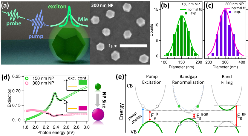
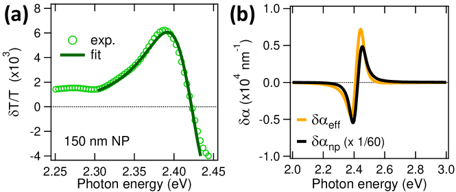
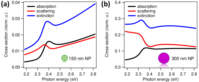
Isolated CsPbBr3 nanoparticles with different average sizes (see distributions in Fig. 1b, c) were deposited on a quartz transparent substrate with an average coverage density =3 NP/m2 Makarov2018 . The samples were optically characterized by measuring the extinction, =, where is the sample transmission. In Fig. 1d we report the extinction, which includes both the scattering and absorption contributions, of samples with 150 and 300 nm average NP diameter (). In both cases, the extinction can be reproduced by the following expression:
| (1) |
where the first term on the right-hand side represents a Fano asymmetric excitonic linewidth with amplitude , centered at , being the exciton binding energy, and with a lineshape controlled by the broadening parameter and the profile index . accounts for the absorption across the semiconducting edge at (see Sec. S2 for more details).
For 150 nm NPs, the small overlap between the excitonic line at -2.4 eV and the Mie resonances results in a moderate asymmetry of the peak in the extinction spectrum (green markers in Fig. 1d), corresponding to -18 (high- resonance). When the NP size is increased (300 nm), the overlap between the Mie modes and the excitonic resonance increases. As a result, the scattering contribution strongly increasesMakarov2018 thus turning the extinction lineshape into a dip (pink markers in Fig. 1d), which corresponds to -0.4 (low- resonance). The separate scattering and absorption contributions to the total extinction of single NPs are discussed in the Supplementary Information.
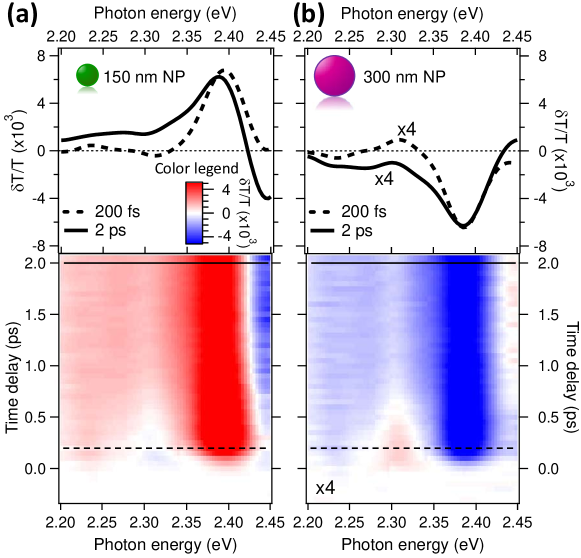
In this work we use 40 fs (FWHM) light pulses at 2.9 eV photon energy to trigger the out-of-equilibrium dynamics in HP NPs. In general, it is known that in bulk semiconductors the sudden photo-generation of high-density non-thermal electrons(holes) within the conduction(valence) band (see Fig. 1e) modifies the electron screening thus shrinking the band gap Bennett1990 . This phenomenon, known as band gap renormalization (BGR), manifests itself into a photo-induced absorption increase below the semiconducting band edge Price2015 , corresponding to a photo-induced dynamical decrease of the effective band gap, =-. Within 1 ps, the electron-electron and electron-phonon interactions drive the relaxation of the non-thermal population and the creation of a long-lived quasi-thermal distribution, described by an effective temperature and chemical potential, which overfills the electron(hole) states at the band edges (see Fig. 1e). The consequent bleaching of the band-edge transitions, known as band filling (BF) or dynamic Burstein-Moss effect Burstein1954 ; Moss1954 , leads to the photo-induced dynamical increase of the effective band gap, =+, until the equilibrium distribution is eventually recovered on the nanosecond timescale via interband recombination Manser2014 . To address the role of the geometry in controlling the modulation of the optical properties consequent to the BGR and BF processes, we performed broadband pump-probe experiments on NPs all the way from Fano high- to low- resonance conditions. The pump-induced relative transmittivity variation, , is measured in the 2.2-2.5 eV energy range by means of a delayed () supercontinuum white light probe detected through a collinear interferometer (GEMINI by NIREOS) Preda2016 ; Preda2017 , as described in the Methods. The energy- and time-dependent is reported for 150 and 300 nm NPs (see Figs. 2a, b). More experimental data for different NP sizes are shown in Fig. S1.
In the Fano high- resonance condition (150 nm, Fig. 2a), the signal is characterized by a short-lived negative component at 2.3 eV and a long-lived signal, which turns from positive to negative at the exciton peak at -2.4 eV. The presence of two different spectral components can be appreciated by plotting spectra at different delays (=0.2 and 2 ps, top panel of Fig. 2a). The negative transmittivity variation at short delays reflects a photo-induced increase of below-gap absorption, which is the signature of the BGR effect, as already observed in thin films Price2015 . On the picosecond timescale this effect decays as a result of hot carrier cooling through electron-phonon interactions Price2015 . As a consequence, after 2 ps the positive(negative) transmittivity variation at ()2.4 eV can be reproduced, over the entire frequency range, by a rigid blue-shift, by =(5.10.4) meV, of the excitonic line in Eq. 1. Such shift is the typical manifestation of the conventional band filling effect, which has been already reported in HP thin-filmsManser2014 . We remark that the transmittivity variation measured in our pump-probe experiment refers to the effective response of the sample, which can be modeled as an inhomogeneous film with CsPbBr3 NPs, with volume filling fraction . Therefore, in order to quantitatively compare our results to previous data on thin films, we extracted the pump-induced shift of the band-gap of the individual nanoparticles () by calculating the scaling factor (), which relates to the measured effective . As described in Section S2, we adopted the Modified Maxwell-Garnett Mie (MMGM) theory Battie2014 for the effective medium, which accounts for size-dispersed spherical particles embedded in a host matrix, to calculate the scaling factor as the ratio between the intrinsic absorption variation of an individual NP and the effective absorption variation of the film. From our analysis, we estimated =6040. Considering that, for small shifts, the transmittivity variation in the proximity of a peak is directly proportional to the shift amplitude, we can thus assume that =(300200) meV, which is in quantitative agreement with data reported in Ref. 10.
The non-equilibrium optical response of CsPbBr3 nanoparticles progressively changes when the NP size is increased and the overlap between the exciton resonance at 2.4 eV and the geometry-controlled continuum of the Mie modes is enhanced. In the Fano low- resonance condition, obtained for 300 nm NP size, the signals associated to both the band gap renormalization and band filling effects are reversed, as shown in Fig. 2b. In this condition, the sub-ps below-gap transmittivity change is positive, thus suggesting a photo-induced decrease of below-gap absorption in opposition to the conventional band gap renormalization effect measured in films and nanoparticles far from the Fano low- resonance condition.
Our results demonstrate that the non-equilibrium optical properties of CsPbBr3 NPs following ultrafast excitation are crucially controlled by the NP size. The photo-generated electron/hole population in the conduction and valence bands gives rise to a photo-induced variation of the far-field optical properties, which qualitatively and quantitatively depends on the interference between the excitonic resonance and the geometrically-controlled Mie modes. To gain further insights into the interplay between non-equilibrium photo-injected free carriers and the geometry-controlled Fano interference, we performed full-vectorial numerical electromagnetic simulations implemented with the finite element method in COMSOL. In these numerical calculations, we considered isolated HP nanospheres deposited on a quartz substrate with refractive index 1.45. The numerical simulations of the full electromagnetic problem go beyond the Mie theory for isolated NPs, which is presented in Section S6, and allow us to account for the NP-substrate interaction that affects spectral position, amplitude, and phase of the resonances in the NP. markovich2014magnetic
The frequency dependent transmittivity variation of the single NP is calculated as = (for details, see Methods). The equilibrium extinction, , is obtained by solving the NP scattering problem and assuming the complex refractive index of bulk CsPbBr3 (extracted from Ref. 27). The out-of-equilibrium extinction, , is obtained by properly modifying the equilibrium optical properties to account for the effect of photo-generated non-equilibrium carriers. More specifically, we assume that the photo-excitation process initially injects an excess density of electrons () and holes () approximately equal to the density of absorbed photons, i.e. . On the sub-picosecond timescale, the photo-injected free carrier density, =+2 (see Methods for calculation of ), overcomes the screening critical concentration, 3.41018 cm-3 (see Sec. S5 of the Supplementary Information) Bennett1990 , thus leading to a photo-induced bandgap renormalization and a related change of the absorption coefficient expressed as Bennett1990 :
| (2) |
Within 1 ps, the carrier-carrier and carrier-phonon interactions lead to the relaxation of the photo-injected free carriers and to the onset of a quasi-thermal effective carriers distribution which completely fills the states at the bottom(top) of the conduction(valence) band. The bleaching of the gap-edge transitions (band filling) manifests itself as Bennett1990 :
| (3) |
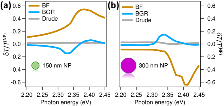
where the effective Fermi-Dirac populations in the valence and conduction bands, and respectively, are controlled by the effective Fermi levels and and by the effective temperature . The photo-induced absorption change related to transition of free carriers within the conduction(valence) band is accounted for by a Drude model, as described in Sec. S5 of the Supplementary Information. We calculated for different NP sizes, namely 150 and 300 nm (Fig. 3a and b, respectively), corresponding to the Fano high- resonance and low- resonance conditions. While the Drude contribution is always negligible (see Fig. 3), the BGR and BF dominate the transmittivity change, as can be evidenced by calculating separately the two contributions to the signal. For both NP sizes, the BGR effect has been estimated by assuming =35 in Eq. 2. The BF effect has been reproduced by assuming that the effective thermal energy of the free carriers is given by the excess energy injected by the pump photons and equally shared between electrons and holes, i.e. 3/2=(-)/2. Considering =2.9 eV and 2.4 eV, we obtain 3000 K. and are then self-consistently calculated (see Eqs. S21 and S22) assuming =2. The results reported in Fig. 3 show that, for 150 nm NP size, the BGR results in an additional below edge absorption (negative ), which is opposite to the signal related to the BF process. In contrast, when the NP size matches the Fano low- resonance condition (300 nm, Fig. 3b), both the BGR and BF contributions to the differential transmittivity variation are of opposite sign as compared to the high- resonant case. Moreover, the results obtained from the simulations are consistent with the experimental data obtained for a wider set of CsPbBr3 NP samples. Indeed, in the case of nanoparticles with average sizes of and , whose extinction spectrum is characterized by a peak (high-) near the exciton line (see Fig. S1a), their out-of-equilibrium optical properties (reported in Fig. S1b, d) exhibit spectral features similar to those reported for NP sample. These numerical results support our experimental findings and demonstrates that the photo-induced modulation of the NP optical properties is controlled by the geometry of the system.
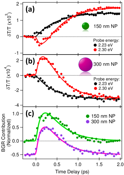
The numerical results reported in Fig. 3 offer important insights into the photophysics of HP NPs and provide a guide for disentangling the BGR and BF dynamics, which experimentally overlap on the picosecond timescale. The results reported in Figs. 3a and 3b indicate that, for both NP sizes, the at 2.2 eV is dominated by the BF effect, whereas the BGR signal is negligible. As a consequence, time traces at this photon energy, although smaller in amplitude with respect to data at higher photon energy, directly reproduce the dynamics of the BF alone. In Figs. 4a and 4b we report =2.23 eV, ) time traces (black dots), which can be fitted by a single exponential function (black lines) with similar time constant =48020 fs. The BGR dynamics can then be retrieved by analyzing the time-traces taken at different photon energies for which the BGR contribution is not negligible. In Fig. 4a and 4b we report =2.3 eV, ) time traces (red dots), which exhibit a multi-exponential behaviour. In Fig. 4c we report the components of the multi-exponential fit which directly represent the time evolution of the actual BGR process; the curves are obtained by subtracting the properly scaled BF contribution from the full dynamics at (see Sec. S4 for more details). For both NP sizes, the build-up time of the BGR signal is 200 fs, whereas the relaxation of the non-thermal carriers responsible for the BGR takes place within 40010 fs, a timescale compatible with the carrier cooling mediated by the coupling to optical phonons Richter2017 . We underline that, in the time-resolved traces, the dynamics of the signal is proportional to the non-equilibrium population within the valence and conduction bands. This population, which is bottlenecked by the presence of the gap, decays on a time scale much longer than the inverse of the exciton linewidth () that accounts for the whole of quasi-elastic scattering processes which reduce the exciton lifetime. The procedure here introduced and based on time- and frequency-resolved optical measurements constitutes a way to disentangle the BGR and BF processes. Our results show that, microscopically, the two processes are almost independent of the NP size, as expected since the exciton Bohr’s radius (7 nm) Protescu2015 is much smaller than the NP size. The observed inversion of the , ) signals in the Fano low- resonance condition is thus a genuine effect of the geometry of the system, which controls the sub-picosecond modulation of the optical properties.
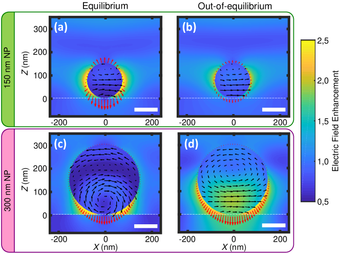
The numerical simulations also reproduce the local electric field enhancement , defined as the ratio between the modulus of the electric field () and the amplitude of the of the incident plane wave (): . Fig. 5 shows equilibrium and out-of-equilibrium at for a single nanoparticle with and diameter size. The black arrows represent the electric field vector for the same excitation parameters used to obtain the plots reported in Fig. 3. For NPs, the equilibrium resonance (panel (a)) is dominated by the electric dipole (ED) mode. The ED spatial pattern is maintained also in out-of-equilibrium conditions (panel (b)). On the other hand, the nature of the resonance dramatically changes for NPs. The electric field distribution in Fig. 5c suggests that both ED and MD (magnetic dipole) resonances contribute to the electromagnetic response at equilibrium, the latter exhibiting a typical field leakage towards the substrate. The MD contribution in NPs, for the probe spectral region considered (), is consistent with the observationMakarovLPR2017 that MD mode takes place when the relation is fulfilled, with being the light wavelength inside the particle. Indeed, from Ref. 27, at , which gives (see multipole modes decomposition for NPs of different sizes in Sec. S6). In the Fano low- resonance condition, the photo-excitation strongly alters the mode spatial distribution (panel (d)) by shifting up the MD center of mass and increasing the ED mode contribution at the NP-substrate interface.
In order to connect the near field solutions to the total scattering, it is instructive to plot the Poynting vector at the NP interface (red arrows). In the Fano high- resonance condition ( NPs in panels (a) and (b)), photo-excitation leads to a quench of the total scattered energy, corresponding to the positive transmittivity variation measured in the experiments. In contrast, the out-of-equilibrium Poynting vector in Fano low- resonance NPs ( NPs in panels (c) and (d)) indicates an overall transient scattering enhancement associated to the ED and MD photo-induced change and corresponding to the negative measured transmittivity variation.
Conclusions
In conclusion, we have studied the photo-induced sub-ps optical modulation of the Fano resonance formed by the coupling of an excitonic state with Mie modes in halide perovskite NPs. In particular, we have demonstrated that the ultrafast modification of the optical properties induced by the band gap renormalization and band filling mechanisms, dramatically depends on the geometry of the NPs. In the low- resonance Fano condition, the contribution of the two effects on the relative transmittivity variation is completely reversed with respect to the high- resonant case and to what was previously observed in thin films and bulk materials Tamming2019 . Importantly, this is the demonstration of the ultrafast control of the optical response in nanoparticles where Mie resonances are coupled with excitons. In previous studies, the ultrafast all-optical switching in Mie-resonant nanoparticles was carried out with standard semiconductors like amorphous silicon Makarov2015 ; Shcherbakov2015 ; Baranov2016 ; Shaltout2019 and gallium arsenide Shcherbakov2017 , for which excitonic effects are negligible at room temperature. Beside the physical effects arising from the coupling between exciton and Mie modes, there is important advantage of high absorption and sharp band-edge in CsPbBr3 perovskites, allowing us to greatly reduce the fluence required to observe ultrafast tuning. CsPbBr3 nanoparticles exhibit an amplitude of the transmittivity modulation that is two order of magnitude larger as compared to that measured in silicon-based Mie resonators under similar photo-excitation conditions Baranov2016 . Although in this work we focused on CsPbBr3 nanoparticles, the results and modeling discussed simply rely on the geometry-driven overlap between the exciton line and the continuum of Mie resonances. As a consequence, the present results can be promptly extended to a wider class of perovskites-based nanonstructures. The present results offer insights into the photophysics of halide perovskite nanoparticles and provide an additional parameter to control their optical properties at frequencies as high as few THz, with impact on perovskite-based optoelectronic devices, metamaterials and switchable nano-antennas.
Methods
Samples
Perovskite NPs are deposited on the ITO and glass substrates according to the following protocol. A solution 1 consists of lead(II) bromide (PbBr2, 36.7 mg, 0.1 mmol) and cesium(I) bromide (CsBr, 21.2 mg, 0.1 mmol) dissolved in 1 mL of anhydrous dimethyl sulfoxide (DMSO). A solution 2 consists of polyethylene oxide (PEO, average Mw 70 000, 10 mg) stirred at 300 rpm in 1 ml of DMSO at 70 for 10 h. 1 and 2 are mixed in 1:3 mass ratio and stirred at 100 for 10 min to give a perovskite-polymer ink. The latter is deposited on precleaned glass and ITO substrates by spin-casting at 1500 rpm for 1 min. The deposited films are annealed at 130 for 3 min to produce NPs with an average size of 150 nm and at 80 for 10 min to obtain NPs with an average size of 300 nm. All the procedures are conducted inside a N2-filled glovebox with both O2 and H2O level not exceeding 1 ppm. Extinction spectra are measured in a UV-vis-NIR spectrophotometer (Shimadzu UV-2600).
Time-Resolved Pump-Probe Spectroscopy
The optical pump-probe set-up is based on a Yb-laser system (Pharos, Light Conversion), which delivers J, fs pulses at central wavelength and 400 kHz repetition rate. A portion of the laser with J energy is used to pump an optical parametric amplifier (Orpheus-F, Light Conversion). The output signal at is frequency doubled to obtain a pump pulse at (), bandwidthPolliCerullo2010 , with nJ energy per pulse that is focused within m spot size (fwhm). The J/cm2 incident pump fluence is such that the average absorbed photon density is (see Sec. S3 for more details). The other portion of the laser is focused on a sapphire crystal to generate a white-light continuum probe ranging from to , which is then reduced to the region - (-) by a colored bandpass glass filter ( ). The pump is modulated by a mechanical chopper working at . The pump pulse is delayed in time with respect to the probe pulse by using a linear motorized stage (Physik Instrumente M403.2DG). The pump and the probe beams are orthogonally polarized: the pump is linearly horizontally polarized, whereas the probe is vertically polarized. The two beams are non-collinearly focused onto the sample: the pump impinges on the sample at normal incidence, while the incident angle of the probe is less than . After the interaction with the sample, the linear and differential transmission spectra (at fixed pump-probe delay) are detected by means of a common-path birefringent interferometer, GEMINI (from NIREOS), which generates two collinear replicas of the incoming light. When the relative delay between the two probe replicas is varied, the light interferogram is obtained on a single-pixel photodiode.
The linear transmission spectrum is obtained by computing the Fourier Transform of the interferogram, while the differential transmission spectrum is retrieved by computing the Fourier Transform of the interferogram demodulated by a lock-in amplifier at the chopping frequency. The pump-induced relative transmittivity variation is defined as , where and are the out-of- and equilibrium transmittivities.
Simulations
We performed full-vectorial numerical simulations implemented with the finite element method in COMSOL. In our simulations, we consider the linear scattering problem of an electric field impinging on isolated CsPbBr3 nanospheres deposited on a quartz substrate. From the simulations, we calculated the absorption and scattering cross-section of the single nanoparticle, and respectively, to obtain the extinction cross-section of the single nanoparticle as bohren2008absorption . The absorption (scattering) cross-section is calculated as (), where () is the rate at which the energy is absorbed (scattered) by the particle and is the incident light intensitybohren2008absorption . The incident field is a linearly polarized plane wave since the focal spot size in the experiment is much larger than the sphere diameter. To obtain the transmittivity of the layer from , we assumed that the nanoparticles are weakly coupled and that they are uniformly distributed on the substrate surface with a coverage distribution density =3 NP/m2. The transmittivity is given by , where the extinction is related to through bohren2008absorption . The equilibrium transmittivity of the nanoparticle is obtained by solving the linear scattering problem for a single CsPbBr3 sphere, where the equilibrium complex refractive index equals the experimental refractive index of CsPbBr3 thin films, reported in Ref.27. The out-of-equilibrium transmittivity is obtained by solving the linear scattering problem for a single CsPbBr3 sphere, where the equilibrium complex refractive index is modified according to Eqs. (2) and (3). This procedure is applied to nanoparticles with diameter of 150 nm and 300 nm.
Acknowledgments
P.F. and C.G, acknowledge financial support from MIUR through PRIN 2015 (Prot. 2015C5SEJJ001) and PRIN 2017 (Prot. 20172H2SC4) programmes. G.F., S.P. and C.G. acknowledge support from Università Cattolica del Sacro Cuore through D.1, D.2.2, and D.3.1 grants. L.C. acknowledges STARS StG project PULSAR. The samples preparation was supported by the Russian Ministry of Science and Higher Education (Project 14.Y26.31.0010). F.B. acknowledges financial support from the IDEXLYON Project-Programme Investissements d’Avenir (ANR-16 -IDEX-0005), France. NIREOS acknowledges financial support from the European Union’s Horizon 2020 research and innovation programme under grant agreement No 814492 (SimDOME).
References
- [1] A Decade of Perovskite Photovoltaics. Nat. Energy, 4(1):1, 2019.
- [2] Yongping Fu, Haiming Zhu, Jie Chen, Matthew P Hautzinger, X.-Y. Zhu, and Song Jin. Metal Halide Perovskite Nanostructures for Optoelectronic Applications and the Study of Physical Properties. Nat. Rev. Mater., 4(3):169–188, 2019.
- [3] Martin A. Green and Henry J. Ho-Baillie, Anita Snaith. The emergence of perovskite solar cells. Nat. Photonics, 8:506, 2014.
- [4] Dong Myung Jang, Kidong Park, Duk Hwan Kim, Jeunghee Park, Fazel Shojaei, Hong Seok Kang, Jae-Pyung Ahn, Jong Woon Lee, and Jae Kyu Song. Reversible halide exchange reaction of organometal trihalide perovskite colloidal nanocrystals for full-range band gap tuning. Nano Lett., 15(8):5191–5199, 2015.
- [5] Loredana Protesescu, Sergii Yakunin, Maryna I. Bodnarchuk, Franziska Krieg, Riccarda Caputo, Christopher H. Hendon, Ruo Xi Yang, Aron Walsh, and Maksym V. Kovalenko. Nanocrystals of cesium lead halide perovskites (CsPbX3, , Br and I): Novel optoelectronic materials showing bright emission with wide color gamut. Nano Lett., 15(6):3692–3696, 2015.
- [6] Hye Ryung Byun, Dae Young Park, Hye Min Oh, Gon Namkoong, and Mun Seok Jeong. Light soaking phenomena in organic - inorganic mixed halide perovskite single crystals. ACS Photonics, 4(11):2813–2820, 2017.
- [7] Christian Wehrenfennig, Giles E. Eperon, Michael B. Johnston, Henry J. Snaith, and Laura M. Herz. High charge carrier mobilities and lifetimes in organolead trihalide perovskites. Adv. Mater., 26(10):1584–1589, 2014.
- [8] Qingfeng Dong, Yanjun Fang, Yuchuan Shao, Padhraic Mulligan, Jie Qiu, Lei Cao, and Jinsong Huang. Electron-Hole Diffusion Lengths 175 m in Solution-Grown CH3NH3PbI3 Single Crystals. Science, 347(6225):967–970, 2015.
- [9] Woon Seok Yang, Jun Hong Noh, Nam Joong Jeon, Young Chan Kim, Seungchan Ryu, Jangwon Seo, and Sang Il Seok. High-performance photovoltaic perovskite layers fabricated through intramolecular exchange. Science, 348(6240):1234–1237, 2015.
- [10] Joseph S. Manser and Prashant V. Kamat. Band filling with free charge carriers in organometal halide perovskites. Nat. Photonics, 8:737, 2014.
- [11] ChuanXiang Sheng, Chuang Zhang, Yaxin Zhai, Kamil Mielczarek, Weiwei Wang, Wanli Ma, Anvar Zakhidov, and Z. Valy Vardeny. Exciton versus free carrier photogeneration in organometal trihalide perovskites probed by broadband ultrafast polarization memory dynamics. Phys. Rev. Lett., 114:116601, Mar 2015.
- [12] Rebecca L. Milot, Giles E. Eperon, Henry J. Snaith, Michael B. Johnston, and Laura M. Herz. Temperature-Dependent Charge-Carrier Dynamics in CH3NH3PbI3 Perovskite Thin Films. Adv. Funct. Mater., 25(39):6218–6227, 2015.
- [13] Ye Yang, David P. Ostrowski, Ryan M. France, Kai Zhu, Jao van de Lagemaat, Joseph M. Luther, and Matthew C. Beard. Observation of a hot-phonon bottleneck in lead-iodide perovskites. Nat. Photonics, 10:53–59, 2015.
- [14] Michael B. Price, Justinas Butkus, Aditya Jellicoe, Tom C.and Sadhanala, Anouk Briane, Jonathan E. Halpert, Katharina Broch, Justin M. Hodgkiss, Justin M. Hodgkiss, Richard H. Friend, and Felix Deschler. Hot-carrier cooling and photoinduced refractive index changes in organic-inorganic lead halide. Nat. Comm., 6 I:8420, 2015.
- [15] Laura M. Herz. Charge-carrier dynamics in organic - inorganic metal halide perovskites. Annu. Rev. of Phys. Chem., 67(1):65–89, 2016.
- [16] Ronnie R. Tamming, Justinas Butkus, Michael B. Price, Parth Vashishtha, Shyamal K. K. Prasad, Jonathan E. Halpert, Kai Chen, and Justin M. Hodgkiss. Ultrafast spectrally resolved photoinduced complex refractive index changes in CsPbX3 perovskites. ACS Photonics, 6(2):345–350, 2019.
- [17] Tania Palmieri, Edoardo Baldini, Alexander Steinhoff, Ana Akrap, Márton Kollár, Endre Horváth, László Forró, Frank Jahnke, and Majed Chergui. Mahan Excitons in Room-Temperature Methylammonium Lead Bromide Perovskites. Nat. Comm., 11(1):850, 2020.
- [18] Behrad Gholipour, Giorgio Adamo, Daniele Cortecchia, Harish N. S. Krishnamoorthy, Muhammad. D. Birowosuto, Nikolay I. Zheludev, and Cesare Soci. Organometallic perovskite metasurfaces. Adv. Mater., 29(9):1604268, 2017.
- [19] Sergey V. Makarov, Valentin Milichko, Elena V. Ushakova, Mikhail Omelyanovich, Andrea Cerdan Pasaran, Ross Haroldson, Balasubramaniam Balachandran, Honglei Wang, Walter Hu, Yuri S. Kivshar, and Anvar A. Zakhidov. Multifold emission enhancement in nanoimprinted hybrid perovskite metasurfaces. ACS Photonics, 4(4):728–735, 2017.
- [20] Yisheng Gao, Can Huang, Chenglong Hao, Shang Sun, Lei Zhang, Chen Zhang, Zonghui Duan, Kaiyang Wang, Zhongwei Jin, Nan Zhang, Alexander V. Kildishev, Cheng-Wei Qiu, Qinghai Song, and Shumin Xiao. Lead halide perovskite nanostructures for dynamic color display. ACS Nano, 12(9):8847–8854, 2018.
- [21] Alexander S. Berestennikov, Pavel M. Voroshilov, Sergey V. Makarov, and Yuri S. Kivshar. Active meta-optics and nanophotonics with halide perovskites. Appl. Phys. Rev., 6(3):031307, 2019.
- [22] E. Y. Tiguntseva, G. P. Zograf, F. E. Komissarenko, D. A. Zuev, A. A. Zakhidov, S. V. Makarov, and Yuri. S. Kivshar. Light-emitting halide perovskite nanoantennas. Nano Lett., 18(2):1185–1190, 2018.
- [23] Sergey Makarov, Aleksandra Furasova, Ekaterina Tiguntseva, Andreas Hemmetter, Alexander Berestennikov, Anatoly Pushkarev, Anvar Zakhidov, and Yuri Kivshar. Halide-perovskite resonant nanophotonics. Adv. Opt. Mater., 7(1):1800784, 2019.
- [24] Manukumara Manjappa, Yogesh Kumar Srivastava, Ankur Solanki, Abhishek Kumar, Tze Chien Sum, and Ranjan Singh. Hybrid lead halide perovskites for ultrasensitive photoactive switching in terahertz metamaterial devices. Adv. Mater., 29(32):1605881, 2017.
- [25] Ashish Chanana, Xiaojie Liu, Chuang Zhang, Zeev Valy Vardeny, and Ajay Nahata. Ultrafast frequency-agile terahertz devices using methylammonium lead halide perovskites. Sci. Adv., 4(5), 2018.
- [26] Can Huang, Chen Zhang, Shumin Xiao, Yuhan Wang, Yubin Fan, Yilin Liu, Nan Zhang, Geyang Qu, Hongjun Ji, Jiecai Han, Li Ge, Yuri Kivshar, and Qinghai Song. Ultrafast control of vortex microlasers. Science, 367(6481):1018–1021, 2020.
- [27] Ekaterina Y. Tiguntseva, Denis G. Baranov, Anatoly P. Pushkarev, Battulga Munkhbat, Filipp Komissarenko, Marius Franckevicius, Anvar A. Zakhidov, Timur Shegai, Yuri S. Kivshar, and Sergey V. Makarov. Tunable hybrid fano resonances in halide perovskite nanoparticles. Nano Lett., 18(9):5522–5529, 2018.
- [28] Maxim R Shcherbakov, Polina P Vabishchevich, Alexander S Shorokhov, Katie E Chong, Duk-Yong Choi, Isabelle Staude, Andrey E Miroshnichenko, Dragomir N Neshev, Andrey A Fedyanin, and Yuri S Kivshar. Ultrafast All-Optical Switching with Magnetic Resonances in Nonlinear Dielectric Nanostructures. Nano Lett., 15(10):6985–6990, oct 2015.
- [29] Maria Maragkou. Ultrafast Responses. Nat. Mater., 14(11):1086, 2015.
- [30] Costas M Soukoulis and Martin Wegener. Past Achievements and Future Challenges in the Development of Three-Dimensional Photonic Metamaterials. Nat. Photonics, 5(9):523–530, 2011.
- [31] Silvia Peruch, Andres Neira, Gregory A. Wurtz, Brian Wells, Viktor A. Podolskiy, and Anatoly V. Zayats. Geometry defines ultrafast hot-carrier dynamics and kerr nonlinearity in plasmonic metamaterial waveguides and cavities. Adv. Opt. Mater., 5(15):1700299, 2017.
- [32] B. R. Bennett, R. A. Soref, and J. A. Del Alamo. Carrier-induced change in refractive index of InP, GaAs and InGaAsP. IEEE J. Quantum Electron., 26:113–122, 1990.
- [33] Elias Burstein. Anomalous optical absorption limit in InSb. Phys. Rev., 93:632–633, 1954.
- [34] T.S. Moss. The interpretation of the properties of indium antimonide. Proc. Phys. Soc., B, 67(306):775–782, 1954.
- [35] Fabrizio Preda, Vikas Kumar, Francesco Crisafi, Diana Gisell Figueroa del Valle, Giulio Cerullo, and Dario Polli. Broadband pump-probe spectroscopy at 20-MHz modulation frequency. Opt. Lett., 41:2970–2973, 2016.
- [36] F. Preda, A. Oriana, J. Rehault, L. Lombardi, A. C. Ferrari, G. Cerullo, and D. Polli. Linear and nonlinear spectroscopy by a common-path birefringent interferometer. IEEE J. Sel. Top. Quant., 23(3):88–96, 2017.
- [37] Y. Battie, A. Resano-Garcia, N. Chaoui, Y. Zhang, and A. En Naciri. Extended maxwell-garnett-mie formulation applied to size dispersion of metallic nanoparticles embedded in host liquid matrix. J. Chem. Phys., 140(4):044705, 2014.
- [38] Dmitry L Markovich, Pavel Ginzburg, AK Samusev, Pavel A Belov, and Anatoly V Zayats. Magnetic dipole radiation tailored by bubstrates: Numerical investigation. Opt. Express, 22(9):10693–10702, 2014.
- [39] Johannes M Richter, Federico Branchi, Franco Valduga de Almeida Camargo, Baodan Zhao, Richard H Friend, Giulio Cerullo, and Felix Deschler. Ultrafast Carrier Thermalization in Lead Iodide Perovskite Probed with Two-Dimensional Electronic Spectroscopy. Nat. Comm., 8(1):376, 2017.
- [40] Sergey V. Makarov, Anastasia S. Zalogina, Mohammad Tajik, Dmitry A. Zuev, Mikhail V. Rybin, Aleksandr A. Kuchmizhak, Saulius Juodkazis, and Yuri Kivshar. Light-induced tuning and reconfiguration of nanophotonic structures. Laser Photonics Rev., 11(5):1700108, 2017.
- [41] Sergey Makarov, Sergey Kudryashov, Ivan Mukhin, Alexey Mozharov, Valentin Milichko, Alexander Krasnok, and Pavel Belov. Tuning of Magnetic Optical Response in a Dielectric Nanoparticle by Ultrafast Photoexcitation of Dense Electron-Hole Plasma. Nano Lett., 15(9):6187–6192, sep 2015.
- [42] Denis G Baranov, Sergey V Makarov, Valentin A Milichko, Sergey I Kudryashov, Alexander E Krasnok, and Pavel A Belov. Nonlinear Transient Dynamics of Photoexcited Resonant Silicon Nanostructures. ACS Photonics, 3(9):1546–1551, sep 2016.
- [43] Amr M. Shaltout, Konstantinos G. Lagoudakis, Jorik van de Groep, Soo Jin Kim, Jelena Vučković, Vladimir M. Shalaev, and Mark L. Brongersma. Spatiotemporal light control with frequency-gradient metasurfaces. Science, 365(6451):374–377, 2019.
- [44] Maxim R. Shcherbakov, Sheng Liu, Varvara V. Zubyuk, Aleksandr Vaskin, Polina P. Vabishchevich, Gordon Keeler, Thomas Pertsch, Tatyana V. Dolgova, Isabelle Staude, Igal Brener, and Andrey A. Fedyanin. Ultrafast All-Optical Tuning of Direct-Gap Semiconductor Metasurfaces. Nat. Comm., 8(1):17, 2017.
- [45] D. Polli, D. Brida, S. Mukamel, G. Lanzani, and G. Cerullo. Effective temporal resolution in pump-probe spectroscopy with strongly chirped pulses. Phys. Rev. A, 82:053809, Nov 2010.
- [46] Craig F Bohren and Donald R Huffman. Absorption and scattering of light by small particles. John Wiley & Sons, New York, 1 edition, 1983.
-
[47]
The absorption coefficient is related to the dielectric function
via
where is the optical frequency and the velocity of light in vacuum. - [48] Frank Stern. Dispersion of the index of refraction near the absorption edge of semiconductors. Phys. Rev., 133:A1653–A1664, 1964.
- [49] Murad Ahmad, Gul Rehman, Liaqat Ali, M. Shafiq, R. Iqbal, Rashid Ahmad, Tahirzeb Khan, S. Jalali-Asadabadi, Muhammad Maqbool, and Iftikhar Ahmad. Structural, electronic and optical properties of CsPbX3 (, Br, I) for energy storage and hybrid solar cell applications. J. Alloy Compd., 705:828 – 839, 2017.
- [50] N. G. Nilsson. Empirical approximations for the fermi energy in a semiconductor with parabolic bands. Appl. Phys. Lett., 33(7):653–654, 1978.
SUPPLEMENTARY INFORMATION
S1 Supplementary Figure

S2 Effective medium theory and model for the differential transmission
In Fig. 1 (main text) we show the fit of the Fano profile (Eq. 1 of the main text) to the experimental extinction () of the and NP samples at equilibrium. In Eq. 1 of the main text, accounts for the absorption across the semiconducting edge and its analytical expression is given by a second-order polynomial function
| (S1) |
where , , and are free parameters.
Given the relation = (where is the sample transmission), it follows that the differential transmission () is:
| (S2) |
where is the differential extinction.
Fig. S2a displays the experimental spectra of the NP sample, taken at delay time . The experimental data (circles) can be reproduced (solid line) by assuming a blue-shift of the Fano profile (Eq. 1 of the main text). As discussed in the main text, the observed blue-shift refers to the whole sample, which can be modelled as an effective medium consisting in CsPbBr3 nanoparticles surrounded by air. To compare the measured band-gap shift () to the values reported in literature for thin films of similar perovskite compounds, we adopt the Modified Maxwell-Garnett Mie model (MMGM) [37], which accounts for the geometry dispersion of Mie resonators, to extract a scaling factor . This scaling factor allows us to estimate the intrinsic bandgap shift of individual nanoparticles () and compare it to results obtained on thin films.
According to the MMGM model, the dielectric function of the effective medium () is related to that of the nanoparticles () and of the surrounding medium () through the relation:
| (S3) |
where is the volume fraction of the inclusion (see Sec. S2.1 for the details of the calculation), is the wavelength in vacuum, is the average diameter of the NPs, is the NPs diameter distribution function, and are the lower and upper limits of the size distribution. The term is the first electric (see Sec. S6.2 for more details) Mie coefficient given by:
| (S4) |
where and are the Riccati - Bessel functions.
We assume that the equilibrium dielectric function of the nanoparticle equals that of the CsPbBr3 thin film (which is extracted from Ref. 27).
According to the experimental distribution of the NPs diameters reported in Fig. 1 of the main text, we assume a normal distribution of diameters given by:
, where is the standard deviation of the distribution.
In the case of the NPs sample, and .
Within the framework of MMGM theory, we calculated the scaling factor as the ratio between the absorption111The absorption coefficient is related to the dielectric function via where is the optical frequency and the velocity of light in vacuum. variation of the nanoparticles () and the absorption variation of the sample (), i.e. =/. Fig. S2b reports the comparison between the variation of the absorption coefficient of the sample (yellow solid line) and of the nanoparticles (black solid line). To calculate we optimize the overlap between the absorption variations at energies smaller than the exciton peak, which is the region investigated by our pump-probe experiment. Following this procedure we obtain = . The error is calculated taking into account the fact that the samples consist in lattices of randomly distributed nanoparticles. The average coverage distribution density is , but it oscillates in the range 15 .
S2.1 Calculation of the volume fraction
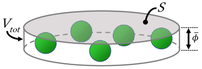
The volume fraction can is estimated as (see Fig. S3):
where is the volume of the single nanoparticle, is the volume of the selected region (the height of the cylinder equals the mean nanoparticle diameter), number of particles within the selected region, is the mean nanoparticle diameter, is the average coverage distribution density, and is area of the base of the selected region. Considering the experimental parameters and , it follows that .
S3 Calculation of the pump photon density
The initial free-carrier density injected by each pump pulse has been evaluated by taking into account the material extinction, the fluence employed in the pump-probe experiment, and the structural properties of the nanoparticles. The incident fluence is /cm2 at . For NPs, the extinction at the pump wavelength is and the equilibrium transmission results equal to . Taking into account the reflection from the substrate (=) and assuming that the energy is absorbed by the nanoparticles, the absorption due to the nanoparticles is . It follows that the absorbed fluence is /cm2 and, therefore, the energy absorbed over an area is . Given an average coverage distribution density of /m2 and assuming a spherical shape for the nanoparticles, which gives a volume , the energy absorbed per unit volume is . Finally, given that the pump is centered at , the photon density per unit volume at the pump wavelength is .
S4 Analysis of the time-resolved traces
The time-resolved traces, at fixed probe energy, are analysed according to the following double-exponential model. This choice is due to the fact that we want to describe the dynamics of the differential signal as the sum of the contributions due to bandgap renormalization (BGR) and band filling (BF). The model is given by the convolution between a gaussian function , describing the experimental time resolution (given by the pump temporal width), and the material response function :
| (S5) |
| (S6) |
In the previous expressions, =40 fs is the FWHM of the pump-laser pulse, is the zero-time offset, is the BGR rise time, is the BGR decay time, is the BF rise time, is the BF decay time, and are the amplitude factors of the two mechanisms.
| Parameter | 150-nm-NP | 300-nm-NP |
|---|---|---|
| 200 10 | 190 10 | |
| 410 10 | 390 10 | |
| 500 20 | 460 20 |
S5 Models of the dynamics of the single nanoparticle optical properties
Here, we report the description of the models adopted to establish the role of the different physiscal phenomena in determining the out-of-equilibrium optical properties of the single nanoparticle. Upon free-carriers injection, the transmission variation is controlled by three main components [32]: the Drude term (D), the band filling (BF) and the bandgap renormalization (BGR) effects. These processes give rise to a modulation of both the refractive index and absorption, as given by:
| (S7a) | |||
| (S7b) | |||
For each process (=D, BGR, BF), the refractive index and absorption variations are constrained by the following Kramers-Krönig relations:
| (S8) |
where is the speed of light in vacuum, is the electron charge, is the Planck’s constant, and P.V. is the Cauchy principal value [32, 48]. As it will be described in the following, these three components depend on the pump-injected free-carriers density . In our analysis, we assume an injected free-carrier density for 150 nm NPs; moreover, the pump-injected free-electron density in the conduction band () is assumed equal to the pump-injected free-holes density in the valence band (), i.e. .
S5.1 Drude
The Drude term represents the physical mechanism for which the photon-absorption promotes a free-carrier to a higher energy state within the same band. The corresponding change in the refractive index is given by:
| (S9) |
where is the reduced-effective mass (, [5]), is the refractive index at equilibrium and is the inverse collision time of the carriers.
S5.2 Bandgap Renormalization
In the case of parabolic bands, the optical absorption of electrons (holes) from the valence (conduction) band to the conduction (valence) band is given by the square-root law:
| (S10) |
where , , and are respectively the band-gap energy, the exciton binding energy and a constant. The bandgap renormalization term is modeled as a rigid translation (red shift) of the absorption curve:
| (S11) |
S5.3 Band Filling
The band filling term implies a free-carriers induced modulation of the interband absorption for photon energies slightly above the nominal bandgap. In presence of free-carriers injection, the variation of the intraband absorption is described by the following expression:
| (S14) |
where
| (S15) |
are the Fermi-Dirac distributions for the electrons in the conduction band and holes in the valence band, respectively. In Eq. S15, is the effective temperature, and denote an energy level in the valence and conduction band, and and are the carrier-dependent quasi-Fermi levels. The effective temperature is computed by considering the excess energy of the pump-excited free-carriers which, in our case, corresponds to (we assume that the energy is equally distributed between electrons and holes, [13]). For a given photon energy , the values of and are uniquely defined on the basis of energy and momentum conservation:
| (S16) |
The value of the carrier-dependent quasi-Fermi levels is computed by the Nilsson approximation [50]:
| (S17) |
and
| (S18) |
where the zero energy level is set at the bottom of the conduction band. and are the effective density of states in the valence and conduction band, respectively, given by
| (S19) |
The refractive index variation due to bandgap renormalization and band filling is obtained after the application of the Kramers-Krönig relations (see Eq. S8). The possible photoinduced variation of interband transitions at high energies, i.e. beyond the experimental accessible energy range, would gives rise to an additional refractive index variation, which is not accounted for by Eq. S14. This contribution is considered by assuming an additional frequency independent refractive index variation, , which can be adjusted to finely match the ratio between the amplitudes of the signals at the energy 2.4 eV for the 150 nm and 300 nm NPs.
S6 Mie-theory of single particle
S6.1 Extinction, Scattering, and Absorption
In order to clarify how scattering and absorption mechanisms contribute to total extinction, we analytically calculated the scattering, extinction and absorption cross-sections (, , and , respectively) of a single sperical CsPbBr3 particle, within the framework of Mie theory [46]. This model applies to the ideal case of isolated nanoparticles in a surrounding medium, but it is instructive to qualitatively address the role of the scattering and absorption processes. The analytical expressions are given by:
| (S20a) | ||||
| (S20b) | ||||
| (S20c) | ||||
where the index is the multipole order, and are the scattering Mie-coefficients of the order , k= is the wave-number in the surrounding medium, is the dielectric function of the surrounding medium, and is the wavelength in vacuum. Assuming that the permeability of the particle equals to that of the surrounding medium, Mie coefficients can be obtained thanks to the following expressions:
| (S21a) | ||||
| (S21b) | ||||
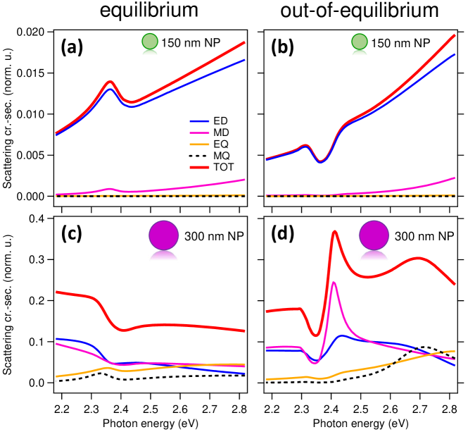
where and are the Riccati - Bessel functions, is the relative refractive index, is the dielectric function of the nanoparticle, is the size parameter, and is the sphere diameter. Basing on these equations and assuming that the dielectric function of a CsPbBr3 nanoparticle equals that of the thin film of the same material (extracted from Ref. 27), we calculate the cross-sections of the CsPbBr3 spherical NPs with diameter of 150 and 300 nm (see Fig. S4). In both cases, near the exciton region, the scattering, characterized by a Fano asymmetric lineshape, dominates the total extinction.
S6.2 Modes Decomposition (equilibrium and out-of-equilibrium)
In this section we describe how multipole decomposition of the scattering cross-section is spectrally modified by the photo-excitation process in the simple case of an isolated nanoparticle in a surrounding medium. The outcome of numerical simulations of the full electromagnetic problem in the realistic configuration (nanoparticle+substrate) is discussed in the main text. In expression S20, (electric) and (magnetic) are the Mie-coefficients of the order . The multipole modes are named according to the order: = stands for dipole mode, 2-quadrupole, 3-octupole, etc. Fig. S5a and c exhibit the scattering cross-section at equilibrium (obtained as described in S6.1), together with the contribution provided by the four strongest multipole modes (dipolar (D) and quadrupolar (Q) modes of magnetic (M) and electric (E) types), for a CsPbBr3 particle with diameter of 150 and 300 nm (panel (a) and (c), respectively). The out-of-equilibrium scattering cross-section (i.e., after photo-excitation) is calculated thanks to expressions S20a, S21 by using a perturbed perovskite dispersion, . The photo-induced variation of the nanoparticles dispersion is obtained as described in Sec. S5. The out-of-equilibrium cross-section, together with the contribution provided by the four strongest multipole modes, are reported in panels (b) and (d) for a CsPbBr3 particle with diameter of 150 and 300 nm, respectively.