Transport experiments in semiconductor-superconductor hybrid Majorana devices
Abstract
As the condensed matter analog of Majorana fermion, Majorana zero-mode is well known as a building block of fault-tolerant topological quantum computing. In this review, we focus on the recent progress of Majorana experiments, especially experiments about semiconductor-superconductor hybrid devices. We first sketch Majorana zero-mode formation from a bottom-up view, which is more suitable for beginners and experimentalist. Then, we survey the status of zero-energy state signatures reported recently, from zero-energy conductance peaks, the oscillations, the quantization, and the interactions with extra-degrees of freedom. This paper also gives prospects on future experiments for advancing one-dimensional semiconductor nanowire-superconductor hybrid materials and devices.
I Majorana and topological quantum computation
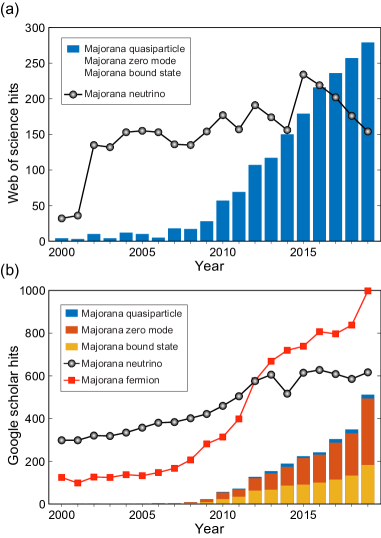
Majorana zero-modes were intensively studied in recent years (see the research trend shown in Fig. 1). There have already been many fantastic review papers about Majoranas Wilczek2009 ; Leijnse2012semi ; Elliott2015 ; Sarma2015 ; Aguado2017 ; Lutchyn2018 ; Prada2019 ; Schuray2020 , mostly for Majorana theories. This review will briefly introduce recent experiment developments of one-dimensional Majorana devices, aiming to give a comprehensive overview and understanding of 1D-Majorana experiments.
We will still briefly introduce some fundamental conceptions of the Majorana theories, and here we start from anyons. Anyons, the two-dimensional particles with fractional statistics Wilczek1982 ; Wilczek1990 , have been predicted to be able to perform quantum computation since the early ’90s Castagnoli1993 . It was further pointed out that anyon-based quantum computing is naturally fault-tolerant (without a large overhead of quantum error-correction) if the anyons’ braiding group is non-Abelian Kitaev2003 . This hardware-level fault-tolerance is endowed by the so-called topological protection Nayak2008 ; Pachos2012 . The quantum information encoded in non-Abelian anyons is only accessible when the anyons are brought together. Unitary operations, in the form of intertwining anyons that are wide apart, remain robust to disturbances, provided that the perturbations are weaker than the topological gap.
Majorana zero-mode (or Majorana bound state, Majorana quasiparticle) is one of the simplest realizations of the non-Abelian anyons (Ising type, specifically). It is a condensed matter physics analog of Majorana particle, an elementary fermion with its antiparticle being itself Majorana1937 ; Cardani2019 . It should be aware that the terminology ‘Majorana’ only means this quasiparticle has a real fermion operator. Majorana first came into condensed matter physics as an operator elucidating the Moore-Read Pfaffian states in fractional quantum Hall systems Moore1991 , and it was then used to refer the zero-energy modes in half-quantum vortices of chiral superconductors Read2000 ; Senthil2000 or superfluids Volovik1999 ; Ivanov2001 .The chiral superconductivity/superfluidity owns an order parameter of + symmetry, and hence, they are also called the -wave superconductivity/superfluidity. Although there are a few candidates of intrinsic -wave superfluids (like 3He-A superfluid phase Volovik2003 ) and superconductors (e.g., Sr2RuO4, CuxBi2Se3, CePt3Si, see the review paper Ref. Sato2017 ), strong evidence of +-pairing is still missing or ambiguous in these systems.
In the meantime, rapid progress has been made in artificial -wave superconductors. In these engineered two-dimensional -wave superconductors, the spin-singlet pairing potential can be induced from an -wave superconductor to a spin-polarized (i.e., spinless) hosting material. Typically, spin-polarized systems, such as ferromagnets, are malicious environments for superconductivity. However, if the hosting material’s spin-texture is a helical type, a finite spin-triplet order parameter can be established at the hybridization interface. With a strong spin-orbit locking effect, a topological insulator in proximity to an -wave superconductor is thus a possible Majorana zero-mode platform Fu2008 . It was then proven a semiconductor with strong spin-orbit interaction can play a similar role to the topological insulator in the presence of a magnet insulator Sau2010 or an in-plane Zeeman field Alicea2010 .
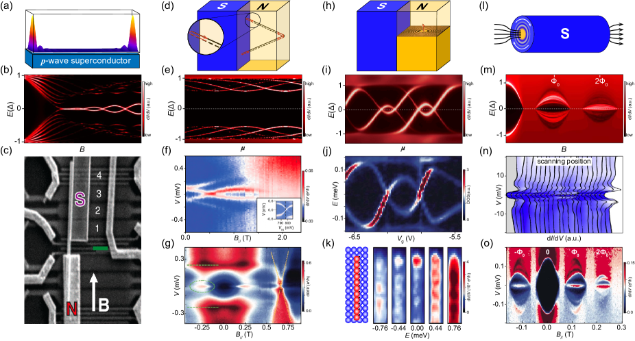
Although Majorana zero-mode was originally envisioned in two-dimensional -wave superconductors, it can also be supported at the phase boundaries (endpoints or domain walls) of one-dimensional systems [Fig. 2(a)]. In fact, the one-dimensional -wave superconductor is one of the earliest and the most straightforward Majorana harboring proposals. The corresponding toy-model is presented as the so-called Kitaev chain model Kitaev2001 . The topological insulator-superconductor hybrids proposed in Ref. Fu2008 mentioned above is an implementation of the Kitaev chain. One-dimensional semiconductor-superconductor nanowires can also support Majorana zero-modes at the end of the wire Lutchyn2010 ; Oreg2010 . Without the hazard of fusion, the adiabatic braiding operations of Majorana zero-mode in a nanowire can be done via a bypassing channel in the wire middle, i.e., a “T”-junction geometry Alicea2011 . Henceforth, the topological quantum computation can be realized in nanowire networks assembled by such “T”-junctions Karzig2017 ; Schrade2018 .
Experimentally pursuing Majorana zero-mode almost immediately began after the theoretical ideas are proposed, and a large number of observations of possible Majorana signatures have been reported. The two most extensively studied veins are the transport measurements in semiconductor-superconductor hybrids Mourik2012 ; Deng2012 ; Rokhinson2012 ; Das2012 ; Churchill2013 ; Finck2013 ; Deng2014 ; Albrecht2016 ; Deng2016 ; Suominen2017 ; Nichele2017 ; GulO2018 ; Vaitiekenas2018 ; Deng2018 ; Shen2018 ; Fornieri2019 ; Ren2019 ; Grivnin2019 ; Anselmetti2019 ; Desjardins2019 ; Vaitiekenas2020 ; Vaitiekenas2020-2 and the scanning-tunneling-microscope based measurements on various materials Perge2014 ; Xu2015 ; Sun2016 ; Pawlak2016 ; Feldman2017 ; Jeon2017 ; Zhang2018s ; Wang2018 ; Liu2018 ; Kong2019 ; Yuan2019 ; Menard2019 ; Zhu2020 ; Wang2020 ; Chen2020 ; Manna2020 ; Liu2020 . As we mentioned above, this review will focus on the first branch, though some relevant experiments of the second branch will also be discussed. Other Majorana quasiparticle experiments, such as 4-periodic supercurrent Bocquillon2017 ; Deacon2017 ; Laroche2019 or chiral Majorana edge states He2017 ; Kayyalha2020 , will not be addressed here.
II Majorana bound state: a bottom-up view
In the above section, we have learned semiconductor-superconductor hybrid nanowire is a possible Majorana platform. To create Majorana zero-modes in such a system, semiconductor nanowires, with a large spin-orbit interaction, should be electronically contacted to superconductors [see the scanning electron microscope image of a typical device in Fig. 2(c)]. Besides the spin-orbit field, an external magnetic field (from a ferromagnet or a coil) is also required to break the time-reversal symmetry. If the external magnetic field is (at least partly) orthogonal to the spin-orbit field, a helical gap can be opened around , with the semiconductor chemical potential. Practically, can be tuned by electric gates near the nanowire. If the Zeeman energy fulfills , Majorana zero-modes can emerge at the end of the wire, with the induced gap [Fig. 2(b)]. A tunneling probe (a normal metal in most cases) with a moderate opaqueness is contacted to the system to detect the formed Majorana zero-modes.
Amidst the Majorana ingredients, the superconducting proximity effect plays a critical role in the engineered topological superconductors. It allows the BCS wavefunction to “leak” out the superconductor into a non-superconducting material in its close vicinity, with some inherited properties of the hosting materials. Since the proximity effect in low-dimension systems always appears along with the formation of Andreev bound states, which have a deep connection to Majorana bound states, we will first elaborate Andreev bound states in-depth below.
Electrons in low-dimensional systems are strongly confined, and the confinements give rise to discrete levels with quantized energies. To distinguish these confined states from their superconducting counterparts, we will refer them as normal bound states in the rest of this review. Just as the word “bound” indicated, the occupying particles of these bound states are coherently bounced back-and-forth by the system boundaries. In a superconductor-normal conductor hybrid system, the so-called Andreev reflection, instead of the normal reflection, occurs when a low-energy incident particle (or hole) travels from the normal conductor into the superconductor. Because of the lack of available states in the superconductor gap , the incident particle (hole) cannot directly propagate into the superconductor. Consequently, the superconductor will retro-reflect (Andreev reflection) a time-reversed hole (particle) with an opposite momentum and spin into the normal conductor. In this way, the superconductor gains (loses) a Cooper pair from (to) the normal conductor. Electron states confined by Andreev reflection are hence called Andreev bound states [see Fig. 2(d)], which are essentially the extension of the superconducting pairing potential out of the superconductor.
Since Andreev reflection is a phase-coherent two-electron process, the energy of Andreev bound states can be modified by adjusting the boundary phase difference (applying a phase-bias across the superconductors) or the picked-phase on a round trip [varying the incident particle momentum via the chemical potential control, see Fig. 2(e)] Houten1991 ; Bena2011 . For example, the phase dependence of Andreev bound state energy in an SNS structure gives , with the transmission coefficient and the phase difference between the two superconductors Beenakker1991 . Obviously, always has a non-zero value without a unitary transmission. However, the Andreev bound states can split in the presence of the Zeeman field and undergo a spin singletdoublet phase transition. The lower-energy branch will cross zero-energy at the phase transition point [see Fig. 2(f)].
Some trivial sub-gap states can stay at zero-energy with zero Zeeman field. For instance, Yu-Shiba-Rusinov states, the bound states formed in superconductors with local magnetic moments Yu1965 ; Shiba1968 ; Rusinov1969 , can have zero-energy when the magnet-screening effect is tuned to a sweet spot [see Figs. 2(h-i)]. The Yu-Shiba-Rusinov states can continuously mutate to ordinary Andreev bound states by varying the local spin arrangement Meng2015 and are also dubbed Andreev bound states in the context of low-energy excitation in superconductors. Generally speaking, the low-energy excitation in Abrikosov vortex, i.e., Caroli-de Gennes-Matricon state Caroli1964 , is another special kind Andreev bound states [see Figs. 2(l)-(n)].
Andreev bound states (including Yu-Shiba-Rusinov states and Caroli-de Gennes-Matricon states) with a broken time-reversal symmetry can be coalesced into Majorana bound states in the presence of a moderate spin-orbit field. Here, we use the word “coalesce” to emphasize that Majorana bound states can directly evolve from Andreev bound states.
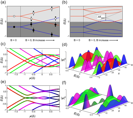
Corresponding to discrete normal bound states, discrete Andreev bound states can form in a 1-D semiconductor-superconductor hybrid wire with a finite length. Those states have different wave vectors and are spin-degenerate at zero magnetic field. As an external magnetic field is applied, each of the Andreev bound states spits into two branches with opposite spins. In the scenario without any interaction between the individual Andreev bound states, one of the two spin-branches (i.e., the inner branch) evolves towards zero-energy as the magnetic field increases. If the bulk superconducting gap can survive at an even higher magnetic field, the inner Andreev bound state will cross zero-energy. In some low-dimensional systems with few states, crossing zero-energy indicates a phase transition from a spin-singlet ground state to a spin-doublet ground state [see Fig. 3(a)]. The crossed Andreev bound state will further evolve monotonously.
However, if the system has a large spin-orbit interaction, level anticrossing occurs [Fig. 3(b)]. It seems that the split low-energy Andreev bound states are pushed back to zero-energy Bommer2019 . One can imagine that the low-energy Andreev bound states can be pinned at zero-energy if there are enough repulsive high-energy states. Moreover, the spin-orbit interaction mixes the wave functions of two states at the level anticrossing point. The state pinned at zero energy effectively comprises the wave vector components from all of the states that it couples to. As shown in Fig. 3(f), from the Fourier transformation point view, the wave function of the zero-energy state can support -function like singularity points at system boundaries. If this picture holds, we get Majorana bound state at those boundaries. This bottom-up view reveals how the Andreev bound states coalesce into Majorana bound states in the presence of the Zeeman field and the spin-orbit field.
From the coalescing Andreev bound state point of view, a long 1D-system with strong spin-orbit interaction can provide enough interacting states to pin the lowest-energy state at zero-energy and guarantee a more -function like wave function of the Majorana state, i.e., a pair of well-decoupled Majorana states. We will come back to this picture in the following sections when discussing different aspects of Majorana signatures.
III Zero-energy conductance peak
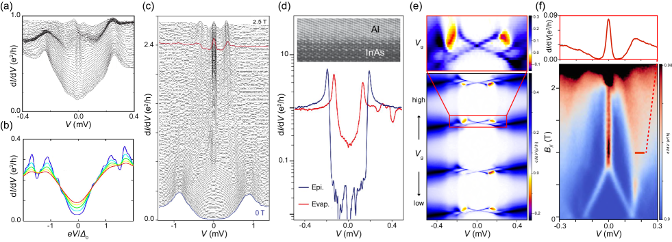
According to theory anticipations, Majorana bound state will emerge in the mid-gap of 1-D -wave superconducting system and give rise to a zero-energy conductance peak if measured by a nearby normal tunneling probe. The first zero-energy conductance peak signature was reported in Ref. Mourik2012 , as shown in Fig. 4(a) [from the device shown in Fig. 2(c)]. Similar signatures were also observed later in Refs. Deng2012 ; Das2012 ; Churchill2013 ; Finck2013 ; Deng2014 . However, in all of these experiments, the zero-energy conductance peaks are accompanied by non-zero sub-gap conductance backgrounds induced by sizable disorders, i.e., the so-called soft-gap problem. Soft-gap could be fatal to Majorana’s application since it will behave like a quasiparticle bath, which can flip the parity of Majorana state and violate the topological protection.
Several effects can cause the soft-gap problem, such as disorders (magnetic/nonmagnetic), BCS broadening effects (temperature), and interface inhomogeneity. Reference Takei2013 theoretically investigated soft-gaps induced by various effects [Fig. 4(b)] and concluded that interface inhomogeneities could be the main reason for the soft-gaps observed in Refs. Mourik2012 ; Deng2012 ; Das2012 ; Churchill2013 ; Finck2013 ; Deng2014 . Therefore, improving the semiconductor-superconductor interface quality is important for observing hard-gap Majorana.
The main obstacle is from the surface oxidization problem. Usually, the semiconductor and the superconductor are fabricated separately. The semiconductor surface will be oxidized in the ambient environment and form an insulating layer. Thus, the surface cleaning process is needed to remove the oxidized layer before evaporating the superconductor on it, via dry etching (plasma ion etching) or wet etching. Inevitable implantation of defects, disorders, or dopant atoms will be induced by ion bombardment or chemical reaction. Extensive efforts for minimizing these damage have been made. For example, optimizing the recipe of InSb nanowire surface retreatment can result in a larger and much cleaner induced gap in an InSb-NbTiN hybrid system GulO2018 . However, as shown in Fig. 4(c), the soft-gap is still visible even at zero-field.
Further breakthrough comes from material synthesizing. Reference Krogstrup2015 reported an in-situ semiconductor-superconductor growth method, in which superconductor (Al) is directly grown on semiconductor nanowire (InAs) without breaking the vacuum. Therefore, surface oxidization/etching and the implanted interface damage are avoided. The atom-by-atom lattice matching guarantees a highly homogeneous interface. As shown by the tunneling spectra in Fig. 4(d), the induced superconductor gap in the full epitaxy hybrid nanowire device is much harder than the gap of the evaporated superconductor nanowire device. With reduced residual sub-gap states, quasiparticle relaxation frequency can be greatly suppressed. In Ref. Higginbotham2015 , the sub-gap negative differential conductance caused by the quasiparticle blocking effect is used to measure the quasiparticle relaxation/poison frequency [Fig. 4(e)]. This frequency can be as low as 102 Hz thanks to the hard gap of the full-epitaxy hybrid nanowire. The hard gap can also persist in a strong parallel magnetic field Deng2016 , and robust zero-energy modes emerge from the clean background [Fig. 4(f)].
However, as noticed in Ref. Vaitiekenas2018 , the induced gap of the full-epitaxy hybrid nanowire in the high electron-density regime (where the effective -factor is large) is still not hard enough. Besides the soft-gap problem, material metallization Antipov2018 ; Mikkelsen2018 ; Reeg2018 , fabrication induced non-uniform potential profile Liu2017 ; Chen2019 , and magnetic field induced quasiparticle poison Higginbotham2015 ; Albrecht2017 also severely hinders the formation of highly decoupled Majorana bound states and their application. Thus, more innovations from material science and nanofabrication technology are required. For instance, in order to provide stronger effective spin-orbit interaction and -factor under metallization, InSb-Al Gazibegovic2017 and InAsxSb1-x-Al Sestoft2018 full epitaxial nanowires have been developed. To improve superconductor quality, long parity lifetime NbTiN devices Woerkom2015 and large gap Sn/Pb/Ta/Nb/V epitaxial shell nanowires Pendharkar2019 ; Carrad2019 ; Khan2020 are under intensive investigation. Moreover, materials beyond 1D, such as 2DEG with epitaxial superconductor films Shabani2016 ; Nichele2017 ; Fornieri2019 and selective-area-grown network structures SAGprl2018 have also been researched. They can avoid wire transferring process induced damages and form more complex structures.
IV Majorana oscillations
As more and more emergent zero-energy conductance peaks in superconductor-semiconductor hybrid systems (and in other platforms) are observed, it is realized that some non-Majorana physics can also give rise to similar conductance peaks. These Majorana-mimicking mechanisms include Kondo effects Lee2012 , weak-antilocalization Pikulin2012 , trivial Andreev/Yu-Shiba-Rusinov/Caroli-de Gennes-Matricon bound states Lee2014 ; Chen2019 ; Scherubl2020 ; Kong2019 . Notably, the difference among trivial sub-gap states and partially coupled Majorana bound states is subtle. Actually, as we will discuss later, it expands a continuum between completely trivial bound states and completely non-trivial bound states. Therefore, it is essential to distinguish a mid-gap state is topological or not via other properties.
Oscillation of zero-energy splitting is one of the unique features of partially coupled Majorana bound states. If a pair of Majorana bound states are separated by a distance , which is comparable to the coherence length of the -wave superconductor , the coupling between the pair of Majorana bound states is finite and leads to a non-zero energy splitting .
The splitting can be estimated by:
| (1) |
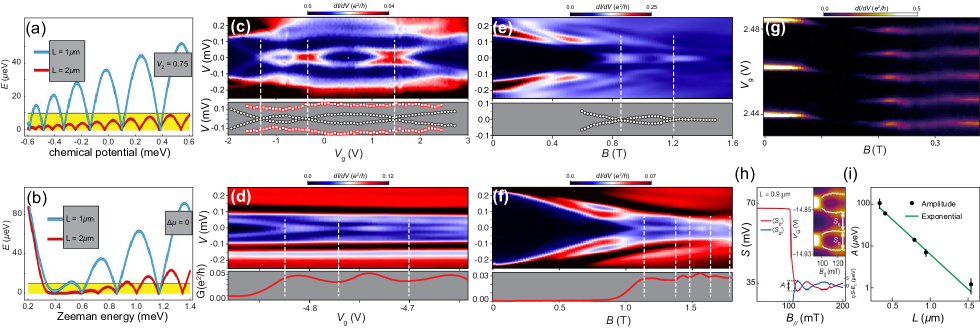
with the effective electron mass and the effective Fermi vector Cheng2009 ; Sarma2012PRB . Indicated by this equation, the Majorana splitting has an oscillating term and an exponential decay term . The decay term is easy to understand because it reflects the coupling is dominated by the effective length of the -wave superconductivity . The oscillatory term is also a direct consequence of the wave nature of Majorana. Here, we would like to relate it to the bottom-up picture shown in Fig. 3 again. The available wave vectors for a one-dimensional object with length are given by (). Therefore, when is varied from to , is changed by and results in an oscillating node. This is consistent with the picture where the merged sub-gap states in Fig. 3 (b) will cross and split until they are pushed back by another interacting state at higher energy. Due to the parabolic dispersion relation, the oscillating period and amplitude will increase when is increased by tuning the chemical potential or the magnetic field [see Figs. 5 (a-b)].
However, the oscillatory pattern in real experiments could be quite different. It is difficult to sweep one parameter and fix all of the other settings. For instance, when one sweeps gate voltage (chemical potential) to vary , semiconductor-superconductor coupling , superconductor coherence length , effective -factor, and spin-orbit coupling strength may all change Antipov2018 ; Mikkelsen2018 ; Reeg2018 , and lead to a more complex oscillating pattern. Reference Sarma2012PRB has also explained the delicate constant density-or-chemical potential problem and concluded that monotonically increase oscillations in most experimental setups will not be seen as Zeeman energy is varied.
In some of the semiconductor-superconductor experiments with emergent mid-gap states, ambiguous oscillating behavior has already been reported. For example, Ref. Churchill2013 reported zero-bias features that oscillate in amplitude as a function of the magnetic field and gate voltage, though the soft-gap background made it difficult to track the sub-gap states.
It is important to emphasize that, as the signature of partially coupled Majorana modes, the low-energy states have to be kept gapped while oscillating. Therefore, we have to characterize the oscillation in a cleaner sub-gap background. As shown in Fig. 5 (c) from Ref. Deng2016 , the gapped characteristic “eye”-feature of the oscillating states as a function of gate voltage can be seen clearly in the hard gap. The characteristic “eye”-shape oscillations have also been observed as a function of the magnetic field, as shown in Figs. 5 (e).
In some cases, the characterization of oscillations in energy is limited by the measurement resolution (and the temperature/coupling broadening). Still, the oscillation can be reflected by the zero-bias conductance amplitude as a characteristic “breathing” fine structure Deng2018 , as shown by the gate and magnetic field dependent measurements in Figs. 5 (d) and (f), respectively. The conductance amplitude breathing is simply because the overlapping of Majorana wavefunction will dramatically influence the Andreev-reflection amplitude at the normal probe-superconductor interface.
The oscillations discussed above are from devices with fixed physical lengths. In Refs. Albrecht2016 and Vaitiekenas2020 , the relations between oscillations and device lengths have been investigated. There, Albrecht et al. and Vaitiekenas et al. monitored the lowest energy sub-gap states of hybrid islands by Coulomb resonance peak space. The oscillations can be measured with a high resolution by averaging a large number of peak spaces. As shown in Figs. 5 (h)-(i)], the oscillation amplitude and device length follows an exponential decay trend.
It is worth emphasizing that the oscillation pattern or the length-dependent should not be considered as a smoking gun signature of Majorana modes alone, but should only serve as evaluation criteria with other signatures together.
V Quantization of majorana conductance
Another spectacular signature of Majorana bound states is the quantization of the tunneling conductance measured from a Fermi lead Law2009 ; Wimmer2011 .
To understand the quantized Majorana conductance, recalling in a normal mesoscopic conductor with a nanoscale constriction (the so-called quantum point contact), the conductance will be quantized to (with ). This conductance quantization requires low temperature and ballistic transport. If the nano-constriction is replaced by two tunneling barriers which are closely separated, unity transmission occurs when the two tunneling barriers have equal transmission. In the perfect resonant regime, quantized conductance can also be achieved at resonance points.
The perfect resonant tunneling is anticipated to always happen at the boundary of a normal lead and a Majorana zero-mode, giving rise to a quantized conductance. The symmetric particle-hole nature of Majorana zero-mode guarantees the equality between the transmission of the incoming particles (holes) to the lead and the transmission of the Andreev-conjugated holes (particles) to the same lead. That is to say, the normal lead close to the Majorana mode plays the role of both an electron lead and a hole lead simultaneously. Ballistic Andreev reflection will lead to a tunneling conductance for each spin-degenerate mode (the BTK model BTK1982 ). For Majorana bound state, the spin degeneracy is lifted, and therefore the quantized Majorana conductance is . This conductance should remain precisely quantized even with disorders. However, quantized Majorana conductance requires the pair of Majorana modes sufficiently separated. Otherwise, interference between two Majorana modes will make the conductance value deviate from . Transparency independent quantized conductance plateau is thus a piece of substantial evidence for Majorana zero-mode.
In a practical experiment, the one-to-one correspondence between quantized conductance and Majorana bound state is unfortunately ambiguous. On the one hand, tunnel barrier with a faulty profile, temperature broadening, multi-band effect, and other dissipations will all cause reductions to the quantized conductance in Majorana point contact structure Pientka2012 ; Rainis2013 ; Liu2017-2 . On the other hand, a zero-energy state with a mundane origin is also possible to give a seemingly quantized conductance plateau along with a single tuning parameter Moore2018 ; Pan2020 . Hence, the robustness of the quantized conductance has to be checked in a high-dimensional parameter space.
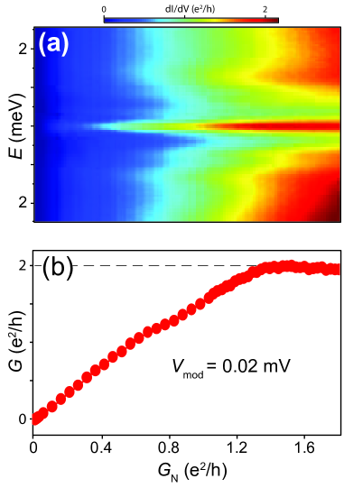
Tunneling conductances measured in the first generations of Majorana devices are substantially lower than the expected bar even at low temperatures ( mK). Tremendous effort has been invested in reducing the dissipation in the hybrid nanowire systems. For example, the hard-gap of full-epitaxy InAs/Al hybrid nanowires can significantly decrease disorder scattering in the Majorana channel. Nevertheless, it is difficult to make a clean tunneling barrier in one-dimensional InAs devices. This is because the conduction channels of InAs nanowires are naturally distributed at material surfaces and severely suffer from surface scatterings. To some degree, this scattering can be relieved in a lateral point contact geometry of a 2D-InAs/Al epitaxial material, in which quantized BTK conductance doubling can be obtained Kjaergaard2016 . One dimensional hybrid wire supporting zero-energy state can be defined out of this 2D system by selectively etching and gating Suominen2017 . In Ref. Nichele2017 , a zero-energy peak with an approximate saturation conductance has been observed.
Nearly quantized conductance plateau has also been measured in a different but relevant system, i.e., a vortex zero mode in an iron-based superconductor Zhu2020 . Emergent zero-energy modes in the cores of FeTe0.55Se0.45 superconductor vortices are probed by a scanning tunneling microscopy tip. The tunneling transmission can be varied by adjusting the tip-sample distance. As the tunneling conductance above the gap increases, the peak-height of the zero-energy vortex mode is found to saturate at a value that is close to or equal to .
Though it is still too early to attribute the quantized conductance plateau to Majorana physics conclusively, the advances made in material growth, device fabrication, and characterization can facilitate Majorana research and its potential application.
VI Interacting Majorana with extra-degrees of freedom
So far, we have discussed the connotations of Majorana physics in one-dimensional hybrid devices by examining the emergence of zero-energy conductance peaks, the oscillations of the peaks, and their quantization. In this section, we will extend the study of Majorana zero-modes to their interactions with some extra-degrees of freedom.
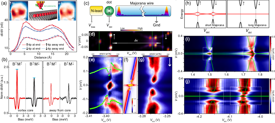
The very first extra freedom is from the probing lead. For instance, in most of the experiments, the probes are Fermi leads with trivial density-of-state distributions. If the metallic probe can be replaced by a superconductor probe, thermal excitation can be greatly suppressed, and the measured conductance quantization should be more robust Peng2015 . Another example is replacing the normal probe with a spin-polarized one. According to the theoretical prediction, for a Majorana end state with a specific local spin-polarization Sticlet2012 , tunneling conductances from probes with different spin-polarizations could be quite different He2014 .
In Refs. Jeon2017 and Sun2016 , spin-polarized scanning tunneling microscopy tips are employed to probe iron-chains on superconductor and topological superconductor vortices, respectively. Both experiments show zero-energy states whose conductances strongly depend on the spin-polarization of the tip [Figs. 7 (a) and (b)].
Similar experiments are also proposed in hybrid nanowire systems Chevallier2018 . The spin-injection can be realized, using a spinful quantum dot between the normal lead and the hybrid nanowire as a spin-filter. Such a quantum dot can form naturally or can be easily defined by electrical gates in the semiconductor constriction part. In the applied magnetic field (which causes phase transition in the hybrid nanowire), the spin-degeneracy of the quantum states in the quantum dot is lifted. Without losing generality, we assume a spin-up level is aligned with the Fermi-level of the normal metal and the hybrid wire. In this case, only spin-up electron transport is allowed without considering high-order cotunneling events [Fig. 7 (c)]. Depending on the alignment details between the dot spin and the Majorana spin, the tunneling conductance to Majorana zero-modes can be greatly modified [Fig. 7 (d)].
Measurements for normal metal-quantum dot-hybrid nanowire devices have been reported in Ref. Deng2018 . As shown in Figs. 7(e) and (g), the conductance corresponding to the emergent zero-energy state highly depends on the spin the quantum dot. At the same time, the conductance corresponding to the sub-gap states with higher energy shows a spin-dependence opposite to the zero-energy mode. This is in line with the prediction from Ref. Chevallier2018 .
Besides providing spin as an interacting degree of freedom, the quantum dot can also serve as a single charge valve, which can be used to estimate the lifetime of Majorana parity Leijnse2011 . Long parity-lifetime of Majorana will result in a sharp negative differential conductance along with one of the Coulomb diamond edge [Fig. 7(f)]. In Figs. 7(e) and (g), such a negative differential conductance pattern (after neglecting the background conductance) identified.
More importantly, a quantum dot coupled to the hybrid wire can be used to estimate Majorana nonlocality Clarke2017 ; Prada2017 ; Schuray2017 . Essentially, the coupled quantum dot can drive a fine-tuned trivial zero-energy state off the sweep spot and split the zero-energy state. Indicated by Fig. 7 (h), a low nonlocality Majorana bound state or a trivial Andreev bound state (red) will be strongly perturbed by a coupled dot level (black). In contrast, a highly nonlocal Majorana bound state will remain unchanged as it crosses the dot level. Such nonlocality measurements have been reported in Refs. Deng2016 ; Deng2018 , see Figs. 7 (i) and (j).
As proposed by many other theoretical works, the quantum dot a versatile tool for Majorana verification Liu2011 ; Zitko2011 ; Ruiz2015 ; Chirla2016 ; Schulenborg2020 ; Ricco2018 and application Gharavi2016 ; Karzig2017 ; Malciu2018 , and this field is still actively researched currently.
VII Other experiments of interests
There is plenty of other experimental progress of 1D-Majorana hybrid devices, which will briefly introduce in this section but will not discuss in-depth details.
First of all, there are a few experiments using different mechanisms or strategies to relax the strict requirements for Majorana materials. The topological phase transition in the semiconductor-superconductor hybrid system is mostly driven by using a Zeeman field of order 1T. Usually, a strong applied magnetic field is incompatible with the superconductor device. In Refs. Fornieri2019 ; Ren2019 ; Yang2019 , phase-controlled topological superconductivity in 2D-material systems are reported. The critical fields for observing zero-energy states are significantly reduced when the superconductor junctions are biased at . Similar but different, it is also demonstrated that quantized vortices with odd-winding numbers in InAs/Al core-shell nanowires can host flux-induced Majorana mode Vaitiekenas2020 . Phase or flux controlled topological superconductivity still requires applying an external magnetic field (though the critical field is reduced). In Ref. Vaitiekenas2020-2 , zero-field topological superconductivity is realized via synthesizing semiconductor, superconductor, and the ferromagnetic insulator together. In this setup, the time-reversal symmetry of the induced superconductivity is broken by the magnetic exchange effect from a EuS layer in the close vicinity. Similarly, it is found that ferromagnetic microstructures with proper magnetic textures can induce a strong spin-orbit field and a Zeeman field for materials with weak intrinsic spin-orbit interactions Desjardins2019 .
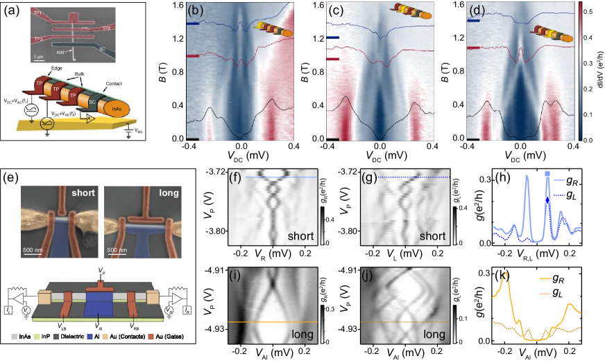
Secondly, devices with multi-terminals have been investigated recently. Most of the devices mentioned above are two-terminal devices, i.e., one probe terminal and one grounding terminal. In this geometry, the probe lead can only peek Majorana zero-mode at one end. Information about the Majorana at the opposite and the bulk p-wave superconductor is, however, still missing. In Ref. Grivnin2019 , the tunneling conductance at the wire-end and the conductance probed in the middle of the wire are monitored simultaneously. A zero-energy state at the end and a reopened gap signature in the middle gap are observed [Figs. 8 (a)-(d)]. End-to-end correlation measurements are performed by Anselmetti et al. in Ref. Anselmetti2019 , where different cross-correlations are found for devices with various length [Figs. 8 (e)-(k)]. However, a clear end-to-end correlation of Majorana conductance has not been reported up to now.
VIII Opportunities and challenges
As a growing field nowadays, experimental research on Majorana hybrid nanowire devices has more opportunities and challenges. On the one hand, conclusive evidence of non-Abelian Majorana zero-mode existence is yet to be found, despite the ambiguous zero-energy state features reviewed above. On the other hand, progress in advanced material growth Pendharkar2019 ; Khan2020 ; Liu2020 ; Gazibegovic2017 ; Carrad2019 ; Krizek2018 ; Lee2019 ; Aseev2019 ; Shabani2016 and more flexible measurement technologies Woerkom2017 ; Tosi2019 ; Spanton2017 ; Razmadze2019 ; Zanten2020 will accelerate Majorana-related physics investigation. More perspective and outlook works can see, for example, Refs. Zhang2019 ; Frolov2020 on transport device design and material synthesizing.
We believe that the profound impact on condensed matter physics and the enormous potential application values of Majorana zero-mode will attract more and more investment, and more fruitful Majorana experiment works can be expected.
Acknowledgment. This work was supported by the National Natural Science Foundation of China (NSFC) (11904399) and the Open Research Fund from State Key Laboratory of High Performance Computing of China (HPCL) (Grant No. 201901-09). M.T.D acknowledges the support from China Great-wall Quantum Laboratory.
References
- (1) References
- (2) Wilczek F. Majorana returns. Nat Phys 2009;5:614-618.
- (3) Leijnse M, Flensberg K. Introduction to topological superconductivity and Majorana fermions. Semicond Sci Technol 2012;27:124003.
- (4) Elliott SR, Franz M. Colloquium : Majorana fermions in nuclear, particle, and solid-state physics. Rev Mod Phys 2015;87:137-163.
- (5) Sarma S Das, Freedman M, Nayak C. Majorana zero-modes and topological quantum computation. Npj Quantum Inf 2015;1:15001.
- (6) Aguado R. Majorana quasiparticles in condensed matter. Riv Del Nuovo Cim 2017;40:523-593.
- (7) Lutchyn RM, Bakkers EPAM, Kouwenhoven LP, Krogstrup P, Marcus CM, Oreg Y. Majorana zero-modes in superconductor-semiconductor heterostructures. Nat Rev Mater 2018;3:52-68.
- (8) Prada E, San-Jose P, de Moor MWA, Geresdi A, Lee EJH, Klinovaja J, et al. From Andreev to Majorana bound states in hybrid superconductor-semiconductor nanowires. arXiv 2019;1911.04512.
- (9) Schuray A, Frombach D, Park S, Recher P. Transport signatures of Majorana bound states in superconducting hybrid structures. Eur Phys J Spec Top 2020;229:593-620.
- (10) Wilczek F. Quantum mechanics of fractional-spin particles. Phys Rev Lett 1982;49:957-959.
- (11) Wilczek F. Fractional statistics and anyon superconductivity. World scientific;1990.
- (12) Castagnoli G, Rasetti M. The notions of symmetry and computational feedback in the paradigm of steady, simultaneous quantum computation. Int J Theor Phys 1993;32:2335-2347.
- (13) Kitaev AY. Fault-tolerant quantum computation by anyons. Ann Phys 2003;303:2-30.
- (14) Nayak C, Simon SH, Stern A, Freedman M, Das Sarma S. Non-Abelian anyons and topological quantum computation. Rev Mod Phys 2008;80:1083-159.
- (15) Pachos JK. Introduction to topological quantum computation. Cambridge University Press; 2012.
- (16) Majorana E. Teoria simmetrica dell’elettrone e del positrone. Nuovo Cim 1937;14:171-184. Translated English version: Majorana E, Maiani L. A symmetric theory of electrons and positrons. Ettore Majorana Scientific Papers. Springer, Berlin, Heidelberg, 2006: 201-233.
- (17) Cardani L. Neutrinoless double beta decay overview. SciPost Phys Proc 2019:024.
- (18) Moore G, Read N. Non-Abelions in the fractional quantum hall effect. Nucl Phys B 1991;360:362-396.
- (19) Read N, Green D. Paired states of fermions in two dimensions with breaking of parity and time-reversal symmetries and the fractional quantum Hall effect. Phys Rev B 2000;61:10267-10297.
- (20) Senthil T, Fisher MPA. Quasiparticle localization in superconductors with spin-orbit scattering. Phys Rev B 2000;61:9690-9698.
- (21) Volovik GE. Fermion zero modes on vortices in chiral superconductors. J Exp Theor Phys Lett 1999;70:609-614.
- (22) Ivanov DA. Non-Abelian statistics of half-quantum vortices in -wave superconductors. Phys Rev Lett 2001;86:268-271.
- (23) Volovik GE. The universe in a helium droplet. Oxford University Press on Demand;2003.
- (24) Sato M, Ando Y. Topological superconductors: A review. Reports Prog Phys 2017;80:076501.
- (25) Fu L, Kane CL. Superconducting proximity effect and Majorana fermions at the surface of a topological Insulator. Phys Rev Lett 2008;100:096407.
- (26) Sau JD, Lutchyn RM, Tewari S, Das Sarma S. Generic new platform for topological quantum computation using semiconductor heterostructures. Phys Rev Lett 2010;104:040502.
- (27) Alicea J. Majorana fermions in a tunable semiconductor device. Phys Rev B 2010;81:125318.
- (28) Deng MT, Vaitiekėnas S, Hansen EB, Danon J, Leijnse M, Flensberg K, et al. Majorana bound state in a coupled quantum-dot hybrid-nanowire system. Science 2016;354:1557-1562.
- (29) Mourik V, Zuo K, Frolov SM, Plissard SR, Bakkers EP a. M, Kouwenhoven LP. Signatures of Majorana fermions in hybrid superconductor-semiconductor nanowire devices. Science 2012;336:1003-1007.
- (30) Lee EJH, Jiang X, Houzet M, Aguado R, Lieber CM, De Franceschi S. Spin-resolved Andreev levels and parity crossings in hybrid superconductor-semiconductor nanostructures. Nat Nanotechnol 2014;9:79-84.
- (31) Pillet J-D, Quay CHL, Morfin P, Bena C, Yeyati a. L, Joyez P. Andreev bound states in supercurrent-carrying carbon nanotubes revealed. Nat Phys 2010;6:965-969.
- (32) Nadj-Perge S, Drozdov IK, Li J, Chen H, Jeon S, Seo J, et al. Observation of Majorana fermions in ferromagnetic atomic chains on a superconductor. Science 2014;346:602-607.
- (33) Vaitiekėnas S, Winkler GW, van Heck B, Karzig T, Deng M-T, Flensberg K, et al. Flux-induced topological superconductivity in full-shell nanowires. Science 2020;367:eaav3392.
- (34) Chen M, Chen X, Yang H, Du Z, Zhu X, Wang E, et al. Discrete energy levels of Caroli-de Gennes-Matricon states in quantum limit in FeTe0.55Se0.45. Nat Commun 2018;9:970.
- (35) Kitaev AY. Unpaired Majorana fermions in quantum wires. Physics-Uspekhi 2001;44:131-136.
- (36) Lutchyn R, Sau J, Das Sarma S. Majorana fermions and a topological phase transition in semiconductor-superconductor heterostructures. Phys Rev Lett 2010;105:077001.
- (37) Oreg Y, Refael G, von Oppen F. Helical liquids and Majorana bound states in quantum wires. Phys Rev Lett 2010;105:177002.
- (38) Alicea J, Oreg Y, Refael G, von Oppen F, Fisher PA. Non-Abelian statistics and topological quantum information processing in 1-D wire networks. Nat Phys 2011;7:412-417.
- (39) Karzig T, Knapp C, Lutchyn RM, Bonderson P, Hastings MB, Nayak C, et al. Scalable designs for quasiparticle-poisoning-protected topological quantum computation with Majorana zero-modes. Phys Rev B 2017;95:235305.
- (40) Schrade C, Fu L. Majorana superconducting qubit. Phys Rev Lett 2018;121:267002.
- (41) Deng MT, Yu CL, Huang GY, Larsson M, Caroff P, Xu HQ. Anomalous zero-bias conductance peak in a Nb-InSb nanowire-Nb hybrid device. Nano Lett 2012;12:6414-6419.
- (42) Rokhinson LP, Liu X, Furdyna JK. The fractional a.c. Josephson effect in a semiconductor-superconductor nanowire as a signature of Majorana particles. Nat Phys 2012;8:795-799.
- (43) Das A, Ronen Y, Most Y, Oreg Y, Heiblum M, Shtrikman H. Zero-bias peaks and splitting in an Al-InAs nanowire topological superconductor as a signature of Majorana fermions. Nat Phys 2012;8:887-895.
- (44) Churchill HOH, Fatemi V, Grove-Rasmussen K, Deng MT, Caroff P, Xu HQ, et al. Superconductor-nanowire devices from tunneling to the multichannel regime: Zero-bias oscillations and magnetoconductance crossover. Phys Rev B 2013;87:241401.
- (45) Finck ADK, Van Harlingen DJ, Mohseni PK, Jung K, Li X. Anomalous modulation of a zero-bias peak in a hybrid nanowire-superconductor device. Phys Rev Lett 2013;110:126406.
- (46) Deng MT, Yu CL, Huang GY, Larsson M, Caroff P, Xu HQ. Parity independence of the zero-bias conductance peak in a nanowire based topological superconductor-quantum dot hybrid device. Sci Rep 2014;4:7261.
- (47) Albrecht SM, Higginbotham AP, Madsen M, Kuemmeth F, Jespersen TS, Nygård J, et al. Exponential protection of zero modes in Majorana islands. Nature 2016;531:206-209.
- (48) Suominen HJ, Kjaergaard M, Hamilton AR, Shabani J, Palmstrøm CJ, Marcus CM, et al. Zero-energy modes from coalescing Andreev states in a two-dimensional semiconductor-superconductor hybrid platform. Phys Rev Lett 2017;119:176805.
- (49) Nichele F, Drachmann ACC, Whiticar AM, O’Farrell ECT, Suominen HJ, Fornieri A, et al. Scaling of Majorana zero-bias conductance peaks. Phys Rev Lett 2017;119:136803.
- (50) Gül Ö, Zhang H, Bommer JDS, de Moor MWA, Car D, Plissard SR, et al. Ballistic Majorana nanowire devices. Nat Nanotechnol 2018;13:192-197.
- (51) Vaitiekėnas S, Deng MT, Nygård J, Krogstrup P, Marcus CM. Effective -factor of subgap states in hybrid Nanowires. Phys Rev Lett 2018;121:037703.
- (52) Deng MT, Vaitiekėnas S, Prada E, San-Jose P, Nygård J, Krogstrup P, et al. Nonlocality of Majorana modes in hybrid nanowires. Phys Rev B 2018;98:085125.
- (53) Shen J, Heedt S, Borsoi F, van Heck B, Gazibegovic S, Op het Veld RLM, et al. Parity transitions in the superconducting ground state of hybrid InSb-Al Coulomb islands. Nat Commun 2018;9:4801.
- (54) Fornieri A, Whiticar AM, Setiawan F, Portolés E, Drachmann ACC, Keselman A, et al. Evidence of topological superconductivity in planar Josephson junctions. Nature 2019;569:89-92.
- (55) Ren H, Pientka F, Hart S, Pierce AT, Kosowsky M, Lunczer L, et al. Topological superconductivity in a phase-controlled Josephson junction. Nature 2019;569:93-98.
- (56) Grivnin A, Bor E, Heiblum M, Oreg Y, Shtrikman H. Concomitant opening of a bulk-gap with an emerging possible Majorana zero-mode. Nat Commun 2019;10:1940.
- (57) Anselmetti GLR, Martinez EA, Ménard GC, Puglia D, Malinowski FK, Lee JS, et al. End-to-end correlated subgap states in hybrid nanowires. Phys Rev B 2019;100:205412.
- (58) Desjardins MM, Contamin LC, Delbecq MR, Dartiailh MC, Bruhat LE, Cubaynes T, et al. Synthetic spin-orbit interaction for Majorana devices. Nat Mater 2019;18:1060-1064.
- (59) Vaitiekėnas S, Liu Y, Krogstrup P, Marcus CM. Zero-field topological superconductivity in ferromagnetic hybrid nanowires. arXiv 2020;2004.02226.
- (60) Xu J-P, Wang M-X, Liu ZL, Ge J-F, Yang X, Liu C, et al. Experimental detection of a Majorana mode in the core of a magnetic vortex inside a topological insulator-superconductor Bi2Te3/NbSe2. Phys Rev Lett 2015;114:017001.
- (61) Sun H-H, Zhang K-W, Hu L-H, Li C, Wang G-Y, Ma H-Y, et al. Majorana zero-mode Detected with Spin Selective Andreev Reflection in the Vortex of a Topological Superconductor. Phys Rev Lett 2016;116:257003.
- (62) Pawlak R, Kisiel M, Klinovaja J, Meier T, Kawai S, Glatzel T, et al. Probing atomic structure and Majorana wavefunctions in mono-atomic Fe chains on superconducting Pb surface. Npj Quantum Inf 2016;2:16035.
- (63) Feldman BE, Randeria MT, Li J, Jeon S, Xie Y, Wang Z, et al. High-resolution studies of the Majorana atomic chain platform. Nat Phys 2017;13:286-291.
- (64) Jeon S, Xie Y, Li J, Wang Z, Bernevig BA, Yazdani A. Distinguishing a Majorana zero-mode using spin-resolved measurements. Science 2017;358:772-776.
- (65) Zhang P, Yaji K, Hashimoto T, Ota Y, Kondo T, Okazaki K, et al. Observation of topological superconductivity on the surface of an iron-based superconductor. Science 2018;360:182-186.
- (66) Wang D, Kong L, Fan P, Chen H, Zhu S, Liu W, et al. Evidence for Majorana bound states in an iron-based superconductor. Science 2018;362:333-335.
- (67) Liu Q, Chen C, Zhang T, Peng R, Yan Y-J, Wen C-H-P, et al. Robust and clean Majorana zero-mode in the vortex core of high-temperature superconductor (Li0.84Fe0.16)OHFeSe. Phys Rev X 2018;8:041056.
- (68) Kong L, Zhu S, Papaj M, Chen H, Cao L, Isobe H, et al. Half-integer level shift of vortex bound states in an iron-based superconductor. Nat Phys 2019;15:1181-1187.
- (69) Yuan Y, Pan J, Wang X, Fang Y, Song C, Wang L, et al. Evidence of anisotropic Majorana bound states in 2M-WS2. Nat Phys 2019;15:1046-1051.
- (70) Ménard GC, Mesaros A, Brun C, Debontridder F, Roditchev D, Simon P, et al. Isolated pairs of Majorana zero-modes in a disordered superconducting lead monolayer. Nat Commun 2019;10:2587.
- (71) Zhu S, Kong L, Cao L, Chen H, Papaj M, Du S, et al. Nearly quantized conductance plateau of vortex zero mode in an iron-based superconductor. Science 2020;367:189-192.
- (72) Wang Z, Rodriguez JO, Jiao L, Howard S, Graham M, Gu GD, et al. Evidence for dispersing one-dimensional Majorana channels in an iron-based superconductor. Science 2020;367:104-108.
- (73) Chen C, Jiang K, Zhang Y, Liu C, Liu Y, Wang Z, et al. Atomic line defects and zero-energy end states in monolayer Fe(Te,Se) high-temperature superconductors. Nat Phys 2020;16:536-40.
- (74) Manna S, Wei P, Xie Y, Law KT, Lee PA, Moodera JS. Signature of a pair of Majorana zero-modes in superconducting gold surface states. Proc Natl Acad Sci 2020:201919753.
- (75) Liu C, Chen C, Liu X, Wang Z, Liu Y, Ye S, et al. Zero-energy bound states in the high-temperature superconductors at the two-dimensional limit. Sci Adv 2020;6:eaax7547.
- (76) Bocquillon E, Deacon RS, Wiedenmann J, Leubner P, Klapwijk TM, Brüne C, et al. Gapless Andreev bound states in the quantum spin Hall insulator HgTe. Nat Nanotechnol 2017;12:137-143.
- (77) Deacon RS, Wiedenmann J, Bocquillon E, Domínguez F, Klapwijk TM, Leubner P, et al. Josephson radiation from gapless Andreev bound states in HgTe-based topological junctions. Phys Rev X 2017;7:021011.
- (78) Laroche D, Bouman D, van Woerkom DJ, Proutski A, Murthy C, Pikulin DI, et al. Observation of the 4-periodic Josephson effect in indium arsenide nanowires. Nat Commun 2019;10:245.
- (79) He QL, Pan L, Stern AL, Burks EC, Che X, Yin G, et al. Chiral Majorana fermion modes in a quantum anomalous Hall insulator-superconductor structure. Science 2017;357:294-299.
- (80) Kayyalha M, Xiao D, Zhang R, Shin J, Jiang J, Wang F, et al. Absence of evidence for chiral Majorana modes in quantum anomalous Hall-superconductor devices. Science 2020;367:64-67.
- (81) Van Houten H, Beenakker CWJ. Andreev reflection and the Josephson effect in a quantum point contact: An analogy with phase-conjugating resonators. Phys B Condens Matter 1991;175:187-197.
- (82) [1] Bena C. Metamorphosis and taxonomy of Andreev bound states. Eur Phys J B 2012;85:196.
- (83) Beenakker CWJ, van Houten H. Josephson current through a superconducting quantum point contact shorter than the coherence length. Phys Rev Lett 1991;66:3056-3059.
- (84) Yu L. Bound state in superconductors with paramagnetic impurities. Acta Phys Sin 1965;21:75-91.
- (85) Shiba H. Classical spins in superconductors. Prog Theor Phys 1968;40:435-451.
- (86) Rusinov A. On the theory of gapless superconductivity in alloys containing paramagnetic impurities. Sov J Exp Theor Phys 1969;29:1101-1106.
- (87) Meng T, Klinovaja J, Hoffman S, Simon P, Loss D. Superconducting gap renormalization around two magnetic impurities: From Shiba to Andreev bound states. Phys Rev B 2015;92:064503.
- (88) Caroli C, De Gennes PG, Matricon J. Bound Fermion states on a vortex line in a type II superconductor. Phys Lett 1964;9:307-309.
- (89) Bommer JDS, Zhang H, Gül Ö, Nijholt B, Wimmer M, Rybakov FN, et al. Spin-orbit protection of induced superconductivity in Majorana nanowires. Phys Rev Lett 2019;122:187702.
- (90) Takei S, Fregoso BM, Hui H-Y, Lobos AM, Das Sarma S. Soft superconducting gap in semiconductor Majorana nanowires. Phys Rev Lett 2013;110:186803.
- (91) Chang W, Albrecht SM, Jespersen TS, Kuemmeth F, Krogstrup P, Nygård J, et al. Hard gap in epitaxial semiconductor-superconductor nanowires. Nat Nanotechnol 2015;10:232-236.
- (92) Krogstrup P, Ziino NLB, Chang W, Albrecht SM, Madsen MH, Johnson E, et al. Epitaxy of semiconductor-superconductor nanowires. Nat Mater 2015;14:400-406.
- (93) Higginbotham AP, Albrecht SM, Kiršanskas G, Chang W, Kuemmeth F, Krogstrup P, et al. Parity lifetime of bound states in a proximitized semiconductor nanowire. Nat Phys 2015;11:1017-1021.
- (94) Antipov AE, Bargerbos A, Winkler GW, Bauer B, Rossi E, Lutchyn RM. Effects of gate-induced electric fields on semiconductor Majorana nanowires. Phys Rev X 2018;8:031041.
- (95) Mikkelsen AEG, Kotetes P, Krogstrup P, Flensberg K. Hybridization at superconductor-semiconductor interfaces. Phys Rev X 2018;8:031040.
- (96) Reeg C, Loss D, Klinovaja J. Metallization of a Rashba wire by a superconducting layer in the strong-proximity regime. Phys Rev B 2018;97:165425.
- (97) Liu C-X, Sau JD, Stanescu TD, Das Sarma S. Andreev bound states versus Majorana bound states in quantum dot-nanowire-superconductor hybrid structures: Trivial versus topological zero-bias conductance peaks. Phys Rev B 2017;96:075161.
- (98) Chen J, Woods BD, Yu P, Hocevar M, Car D, Plissard SR, et al. Ubiquitous non-Majorana zero-bias conductance peaks in nanowire devices. Phys Rev Lett 2019;123:107703.
- (99) Albrecht SM, Hansen EB, Higginbotham AP, Kuemmeth F, Jespersen TS, Nygård J, et al. Transport signatures of quasiparticle poisoning in a Majorana island. Phys Rev Lett 2017;118:137701.
- (100) Gazibegovic S, Car D, Zhang H, Balk SC, Logan JA, de Moor MWA, et al. Epitaxy of advanced nanowire quantum devices. Nature 2017;548:434-438.
- (101) Sestoft JE, Kanne T, Gejl AN, von Soosten M, Yodh JS, Sherman D, et al. Engineering hybrid epitaxial InAsSb/Al nanowires for stronger topological protection. Phys Rev Mater 2018;2:044202.
- (102) van Woerkom DJ, Geresdi A, Kouwenhoven LP. One minute parity lifetime of a NbTiN Cooper-pair transistor. Nat Phys 2015;11:547-50.
- (103) Pendharkar M, Zhang B, Wu H, Zarassi A, Zhang P, Dempsey CP, et al. Parity-preserving and magnetic field resilient superconductivity in indium antimonide nanowires with tin shells arXiv 2019:1912.06071.
- (104) Carrad DJ, Bjergfelt M, Kanne T, Aagesen M, Krizek F, Fiordaliso EM, et al. Shadow epitaxy for in situ growth of generic semiconductor/superconductor hybrids. Adv Mater 2020;32:1908411.
- (105) Khan SA, Lampadaris C, Cui A, Stampfer L, Liu Y, Pauka SJ, et al. Highly Transparent gatable superconducting shadow junctions. ACS Nano 2020:acsnano.0c02979.
- (106) Shabani J, Kjaergaard M, Suominen HJ, Kim Y, Nichele F, Pakrouski K, et al. Two-dimensional epitaxial superconductor-semiconductor heterostructures: A platform for topological superconducting networks. Phys Rev B 2016;93:155402.
- (107) Vaitiekėnas S, Whiticar AM, Deng M-T, Krizek F, Sestoft JE, Palmstrøm CJ, et al. Selective-area-grown semiconductor-superconductor hybrids: A basis for topological networks. Phys Rev Lett 2018;121:147701.
- (108) Das Sarma S, Sau JD, Stanescu TD. Splitting of the zero-bias conductance peak as smoking gun evidence for the existence of the Majorana mode in a superconductor-semiconductor nanowire. Phys Rev B 2012;86:220506.
- (109) Lee EJH, Jiang X, Aguado R, Katsaros G, Lieber CM, De Franceschi S. Zero-bias anomaly in a nanowire quantum dot coupled to superconductors. Phys Rev Lett 2012;109:186802.
- (110) Pikulin DI, Dahlhaus JP, Wimmer M, Schomerus H, Beenakker CWJ. A zero-voltage conductance peak from weak antilocalization in a Majorana nanowire. New J Phys 2012;14:125011.
- (111) Scherübl Z, Fülöp G, Moca CP, Gramich J, Baumgartner A, Makk P, et al. Large spatial extension of the zero-energy Yu-Shiba-Rusinov state in a magnetic field. Nat Commun 2020;11:1834.
- (112) Cheng M, Lutchyn R, Galitski V, Das Sarma S. Splitting of Majorana-fermion modes due to intervortex tunneling in a superconductor. Phys Rev Lett 2009;103:2-5.
- (113) Law KT, Lee PA, Ng TK. Majorana Fermion Induced Resonant Andreev Reflection. Phys Rev Lett 2009;103:237001.
- (114) Wimmer M, Akhmerov a. R, Dahlhaus JP, Beenakker CWJ. Quantum point contact as a probe of a topological superconductor. New J Phys 2011;13:053016.
- (115) Blonder GE, Tinkham M, Klapwijk TM. Transition from metallic to tunneling regimes in superconducting microconstrictions: Excess current, charge imbalance, and supercurrent conversion. Phys Rev B 1982;25:4515-32.
- (116) Pientka F, Kells G, Romito A, Brouwer PW, von Oppen F. Enhanced zero-bias Majorana peak in the differential tunneling conductance of disordered multi-subband quantum-wire/superconductor junctions. Phys Rev Lett 2012;109:227006.
- (117) Rainis D, Trifunovic L, Klinovaja J, Loss D. Towards a realistic transport modeling in a superconducting nanowire with Majorana fermions. Phys Rev B 2013;87:24515.
- (118) Liu C-X, Sau JD, Das Sarma S. Role of dissipation in realistic Majorana nanowires. Phys Rev B 2017;95:054502.
- (119) Moore C, Stanescu TD, Tewari S. Two-terminal charge tunneling: Disentangling Majorana zero-modes from partially separated Andreev bound states in semiconductor-superconductor heterostructures. Phys Rev B 2018;97:165302.
- (120) Pan H, Cole WS, Sau JD, Das Sarma S. Generic quantized zero-bias conductance peaks in superconductor-semiconductor hybrid structures. Phys Rev B 2020;101:024506.
- (121) Kjaergaard M, Nichele F, Suominen HJ, Nowak MP, Wimmer M, Akhmerov AR, et al. Quantized conductance doubling and hard gap in a two-dimensional semiconductor-superconductor heterostructure. Nat Commun 2016;7:12841.
- (122) Chevallier D, Szumniak P, Hoffman S, Loss D, Klinovaja J. Topological phase detection in Rashba nanowires with a quantum dot. Phys Rev B 2018;97:045404.
- (123) Leijnse M, Flensberg K. Scheme to measure Majorana fermion lifetimes using a quantum dot. Phys Rev B 2011;84:140501.
- (124) Peng Y, Pientka F, Vinkler-Aviv Y, Glazman LI, von Oppen F. Robust Majorana conductance peaks for a superconducting lead. Phys Rev Lett 2015;115:266804.
- (125) Sticlet D, Bena C, Simon P. Spin and Majorana polarization in topological superconducting wires. Phys Rev Lett 2012;108:096802.
- (126) He JJ, Ng TK, Lee PA, Law KT. Selective equal-spin Andreev reflections induced by Majorana fermions. Phys Rev Lett 2014;112:037001.
- (127) Clarke DJ. Experimentally accessible topological quality factor for wires with zero energy modes. Phys Rev B 2017;96:201109.
- (128) Prada E, Aguado R, San-Jose P. Measuring Majorana nonlocality and spin structure with a quantum dot. Phys Rev B 2017;96:085418.
- (129) Schuray A, Weithofer L, Recher P. Fano resonances in Majorana bound states-quantum dot hybrid systems. Phys Rev B 2017;96:085417.
- (130) Liu DE, Baranger HU. Detecting a Majorana-fermion zero mode using a quantum dot. Phys Rev B 2011;84:201308.
- (131) Žitko R. Detection of Majorana edge states in topological superconductors through non-Fermi-liquid effects induced in an interacting quantum dot. Phys Rev B 2011;83:195137.
- (132) Ruiz-Tijerina DA, Vernek E, Dias da Silva LGG V., Egues JC. Interaction effects on a Majorana zero-mode leaking into a quantum dot. Phys Rev B 2015;91:115435.
- (133) Chirla R, Moca CP. Fingerprints of Majorana fermions in spin-resolved subgap spectroscopy. Phys Rev B 2016;94:045405.
- (134) Schulenborg J, Flensberg K. Absence of supercurrent sign reversal in a topological junction with a quantum dot. Phys Rev B 2020;101:014512.
- (135) Ricco LS, Campo VL, Shelykh IA, Seridonio AC. Majorana oscillations modulated by Fano interference and degree of nonlocality in a topological superconducting-nanowire-quantum-dot system. Phys Rev B 2018;98:075142.
- (136) Gharavi K, Hoving D, Baugh J. Readout of Majorana parity states using a quantum dot. Phys Rev B 2016;94:155417.
- (137) Malciu C, Mazza L, Mora C. Braiding Majorana zero-modes using quantum dots. Phys Rev B 2018;98:165426.
- (138) Yang G, Lyu Z, Wang J, Ying J, Zhang X, Shen J, et al. Protected gap closing in Josephson trijunctions constructed on Bi2Te3. Phys Rev B 2019;100:180501.
- (139) Krizek F, Sestoft J E, Aseev P, et al. Field effect enhancement in buffered quantum nanowire networks. Phys Rev M 2018;2:093401.
- (140) Lee J S, Choi S, Pendharkar M, et al. Selective-area chemical beam epitaxy of in-plane InAs one-dimensional channels grown on InP (001), InP (111) B, and InP (011) surfaces. Phys Rev M 2019, 3(8): 084606.
- (141) Aseev P, Wang G, Binci L, Singh A, Martí-Sánchez S, Botifoll M, et al. Ballistic InSb nanowires and networks via metal-sown selective area growth. Nano Lett 2019;19:9102-9111.
- (142) van Woerkom DJ, Proutski A, van Heck B, Bouman D, Väyrynen JI, Glazman LI, et al. Microwave spectroscopy of spinful Andreev bound states in ballistic semiconductor Josephson junctions. Nat Phys 2017;13:876-81.
- (143) Tosi L, Metzger C, Goffman MF, Urbina C, Pothier H, Park S, et al. Spin-orbit splitting of Andreev states revealed by microwave spectroscopy. Phys Rev X 2019;9:011010.
- (144) Spanton EM, Deng M, Vaitiekėnas S, Krogstrup P, Nygård J, Marcus CM, et al. Current-phase relations of few-mode InAs nanowire Josephson junctions. Nat Phys 2017;13:1177-81.
- (145) Razmadze D, Sabonis D, Malinowski FK, Ménard GC, Pauka S, Nguyen H, et al. Radio-frequency methods for Majorana-based quantum devices: Fast charge sensing and phase-diagram mapping. Phys Rev Appl 2019;11:064011.
- (146) van Zanten DMT, Sabonis D, Suter J, Väyrynen JI, Karzig T, Pikulin DI, et al. Photon-assisted tunnelling of zero modes in a Majorana wire. Nat Phys 2020;16:663-8.
- (147) Zhang H, Liu DE, Wimmer M, Kouwenhoven LP. Next steps of quantum transport in Majorana nanowire devices. Nat Commun 2019;10:5128.
- (148) Frolov SM, Manfra MJ, Sau JD. Topological superconductivity in hybrid devices. Nat Phys 2020;16:718-24.