Optical response of noble metal nanostructures: Quantum surface effects in crystallographic facets
Abstract
Noble metal nanostructures are ubiquitous elements in nano-optics, supporting plasmon modes that can focus light down to length scales commensurate with nonlocal effects associated with quantum confinement and spatial dispersion in the underlying electron gas. Nonlocal effects are naturally more prominent for crystalline noble metals, which potentially offer lower intrinsic loss than their amorphous counterparts, and with particular crystal facets giving rise to distinct electronic surface states. Here, we employ a quantum-mechanical model to describe nonclassical effects impacting the optical response of crystalline noble-metal films and demonstrate that these can be well-captured using a set of surface-response functions known as Feibelman -parameters. In particular, we characterize the -parameters associated with the (111) and (100) crystal facets of gold, silver, and copper, emphasizing the importance of surface effects arising due to electron wave function spill-out and the surface-projected band gap emerging from atomic-layer corrugation. We then show that the extracted -parameters can be straightforwardly applied to describe the optical response of various nanoscale metal morphologies of interest, including metallic ultra-thin films, graphene-metal heterostructures hosting extremely confined acoustic graphene plasmons, and crystallographic faceted metallic nanoparticles supporting localized surface plasmons. The tabulated -parameters reported here can circumvent computationally expensive first-principles atomistic simulations to describe microscopic nonlocal effects in the optical response of mesoscopic crystalline metal surfaces, which are becoming widely available with increasing control over morphology down to atomic length scales for state-of-the-art experiments in nano-optics.
keywords:
American Chemical Society, LaTeXfont=sf,small \alsoaffiliationCenter for Nano Optics, University of Southern Denmark, Campusvej 55, DK-5230 Odense M, Denmark \alsoaffiliationICREA — Institució Catalana de Recerca i Estudis Avançats, Passeig Lluís Companys 23, 08010 Barcelona, Spain \alsoaffiliationDanish Institute for Advanced Study, University of Southern Denmark, Campusvej 55, DK-5230 Odense M, Denmark \alsoaffiliationDanish Institute for Advanced Study, University of Southern Denmark, Campusvej 55, DK-5230 Odense M, Denmark \abbreviationsIR,NMR,UV
1 Introduction
Metals support collective oscillations of their conduction electrons, known as plasmons, with light-trapping and manipulation capabilities at nanometer length scales, i.e., well below the diffraction limit imposed by traditional optics 1, 2. The wealth of fundamental explorations in plasmonics over the last couple of decades has contributed to shape the field of nano-optics 3, holding great promises for light-based technologies including theranostics 4, 5, photocatalysis 6, 7, plasmonic colors 8, solar energy harvesting 9, 10, and quantum information 11, 12, 13. Advances in modern nanofabrication techniques have driven plasmonics research further by enabling the realization of nano-optical devices that operate on deep-subwavelength scales 14, 15. As current capabilities can routinely pattern metallic nanostructures down to the few-nanometer regime 16, 17, 18, where the frontiers of quantum and classical physics coalesce, new routes towards next-generation plasmon-based technologies begin to emerge, while also posing new challenges in understanding and modeling their optical response at nanometric scales 19, 13.
The realization of thin crystalline noble-metal films 20, 21, 22, 23 is key to cutting-edge explorations of novel plasmonic devices: metallic nanostructures with a high degree of crystallinity are anticipated to suffer reduced Ohmic losses when compared to their amorphous counterparts 24, with the recent observation of plasmons in few-atom-thick crystalline silver films partially confirming this intuitive concept 18. Furthermore, it is well-established in surface science 25 that (111) noble metal surfaces possess Shockley surface states 26, whose features resemble those of a two-dimensional electron gas (2DEG). Shockley surface states can support 2D-like plasmon modes 27 that can be characterized, e.g., by angle-resolved spectroscopy 28, 29, 30, while they can potentially play a role in near-field light–matter interactions at such surfaces.
First-principles simulation methods capture nonclassical effects in the optical response of ultra-thin metal films or few-atom metal clusters 31, 32, but necessitate intensive computational effort that rapidly becomes unfeasible for structures with characteristic sizes ; unfortunately, precision within is what is currently afforded by state-of-the-art top-down nanofabrication techniques. One of the overarching challenges in theoretical nano-optics is thus to describe the optical properties of nanostructured metals by solving Maxwell’s equations while accounting—in the response functions entering the constitutive relations—for quantum-mechanical effects that emerge when electrons are confined in low-dimensional systems, ideally without resorting to overly-demanding numerical approaches that obscure the underlying physics. Fortunately, the situation is somewhat simplified in metals by their ability to effectively screen electromagnetic fields, which leads to an optical response dominated by surface effects. In this context, the concept of microscopic surface-response functions, like the Feibelman -parameters 33, 34, 35, 36, 37, 38, offers a practical and scalable recipe to simultaneously incorporate quantum mechanical phenomena, such as electronic spill-out, nonlocal effects, and surface-enabled Landau damping, into the optical response of metal nanostructures 33, 34, 35, 36, 39, as has been recently demonstrated experimentally 40.
Here, we apply a quantum-mechanical framework that describes the metal as a vertical stack of (homogeneous) atomic layers which are modeled as a realistic one-dimensional (1D) potential. The wave functions obtained by solving the corresponding Schrödinger equation are then used to compute the nonlocal optical response of selected noble metal (gold, silver, and copper) films with specific crystallographic orientations—namely, the (100) and (111) facets—from which we extract the associated Feibelman -parameters. We demonstrate that the -parameters obtained for a thick film (tantamount to a semi-infinite metal), once tabulated (as we do here), can be straightforwardly incorporated into a wide range of electromagnetic problems, ranging from analytical solutions for simple geometries to full-wave numerical electromagnetic solvers of realistic particles, to accurately describe intrinsic quantum mechanical effects affecting the system’s optical response 35, 40. We anticipate that the results presented herein can be widely deployed to describe ongoing experiments and engineer future nanoscale plasmonic devices.
2 Results and discussion
Classically, the metal response to a monochromatic electromagnetic field of frequency can be described by the Drude model through its local-response dielectric function 41
| (1) |
where is an ad hoc correction that accounts for the screening associated with the core electrons in the metal, while the second term describes the response of free electrons characterized by a plasma frequency and a phenomenological scattering rate typically extracted from experiments. To maintain fidelity with experimental data, we follow ref 41 and construct by subtracting the free-electron component from the experimentally tabulated dielectric function 42, , so that ; the parameters used to characterize the noble metals that will be considered in this work, namely silver (Ag), gold (Au), and copper (Cu), are specified in Table 1 below.
| Material | (eV) | (eV) |
|---|---|---|
| Ag | 9.17 | 0.021 |
| Au | 9.06 | 0.071 |
| Cu | 8.88 | 0.103 |
In classical electrodynamics, a metal surface is commonly described by a dielectric function that changes abruptly from the bulk, local dielectric function of the metal, , to that of the adjacent dielectric, . However, this naive prescription can be augmented with -parameter-corrected boundary conditions that incorporate quantum effects associated with the optical response of metal surfaces. Specifically, for a -polarized electromagnetic field impinging on a metal surface from the dielectric side, the nonretarded reflection and transmission coefficients read 34, 35, 36, 37
| (2a) | ||||
| (2b) | ||||
respectively. Here, is the in-plane wave vector (i.e., parallel to the interface), while and denote the frequency-dependent, complex-valued quantum surface-response functions introduced by Feibelman 33, 34, 35, 36 (see Methods). On the other hand, for -polarized light impinging on the interface from the metal side, the corresponding nonretarded reflection and transmission coefficients read
| (3a) | ||||
| (3b) | ||||
Note that, in general, when , where . Equipped with eqs 2 and 3, the overall Fabry–Pérot (FP)-like reflection coefficient of the composite dielectric–metal–dielectric heterostructure can be determined via
| (4) |
where denotes the metal film thickness.
The above quantum-surface-corrected description only requires as inputs the Feibelman response functions, and , which can be obtained for a particular dielectric–metal interface either experimentally 40 or from sophisticated quantum mechanical methods [e.g., time-dependent density-functional theory (TDDFT) or empirical quantum-corrected models]. Here we obtain the d-parameters associated with crystalline noble metal surfaces from nonclassical optical response simulations of their reflection coefficients based on the random-phase approximation (RPA), employing the QM model reported in ref 43 and detailed in the Methods section. More specifically, we construct the RPA susceptibility from single-particle wave functions satisfying the Schrödinger equation for a one-dimensional (1D) phenomenological potential characterizing each material 44; this so-called atomic layer potential (ALP) is fitted to reproduce salient features of the bulk and semi-infinite surface electronic structures, so that the ALP-RPA description captures the effects of electronic band structure, electron spill-out, binding energies, and transverse atomic corrugation in the optical response of layered Ag, Au, and Cu films with (100) or (111) crystallographic orientation (see Table 3). See the Methods section for a comprehensive description of the calculation, in which the metal background polarizability incorporating core electron screening is also included when describing the electron-electron interaction.
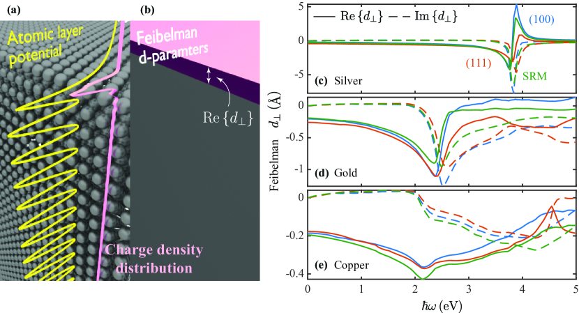
Using the ALP-RPA model, we follow the prescription outlined in the Methods section to extract the Feibelman -parameters presented in Figure 1. The associated with crystalline noble metal surfaces are contrasted with those obtained within the specular reflection model (SRM), first proposed by Ritchie and Marusak to study nonlocal effects on surface plasmon dispersion 45, and later generalized by others to deal with more complex structures 45, 46, 47, 41, 36; the SRM—also known as the semiclassical infinite barrier model (SCIB)—incorporates bulk spatial dispersion (i.e., nonlocality) but assumes a homogeneous electron gas and thus neglects atomic corrugations. In the case of the (100) orientation and the SRM, the absence of surface currents for charge-neutral materials fixes 33, while is introduced heuristically in order to incorporate the response of the Shockley surface states in the (111) facet; as explained in Methods, when extracting for the (111) facets we explicitly omit intraband transitions involving surface states to avoid double-counting the effect of the 2DEG. The Feibelman -parameters presented in Figure 1 clearly distinguish the surface response functions of a metal’s crystallographic facets. In particular, there are two main regions at low energies ( eV) and at energies around where the classical nonretarded surface plasmon is spectrally centered.
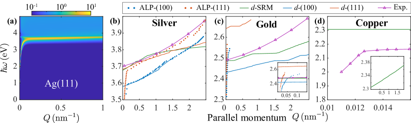
Nonretarded surface plasmon dispersion. Equipped with the -parameters of various noble metals and their crystal facets, along with the analytical expression of eq 2, we illustrate their ability to reproduce the nonretarded surface plasmon dispersion (given by the poles of ) obtained directly from the ALP. While the ALP method actually describes a crystalline metal film of finite thickness, we obtain well-converged results for monolayers,. Figure 2a shows the loss function for silver with a (111) crystallographic orientation in the ALP model as a function of optical in-plane wave vector and energy; peaks in indicate the surface plasmon dispersion, which tends toward zero frequency for small , in agreement with eq 4 for a film of finite thickness and non-vanishing . Figures 2b–d display the nonretarded surface plasmon dispersion for Ag, Au, and Cu, obtained from the ALP (colored dots) along with the Feibelman -parameter (solid curves), together with available experimental data 50, 48, 49.
Here, the -parameter-results have been extracted by comparing eq 2 with the ALP reflection coefficient in the thick-film limit; this procedure, however, needs to be carried out judiciously as the conditions and must be simultaneously fulfilled. Chiefly, our results show that the optical response of a metal surface is determined by the surface’s specific crystallographic orientation and that its surface response can be well-described in terms of the Feibelman -parameter, as evidenced by the overlapping dispersion relation calculated via the ALP model.
From eq 2, it follows that the nonclassical surface plasmon dispersion in the nonretarded regime—keeping only terms up to first-order in —exhibits an approximately linear behavior with in-plane wave vector , namely 37, 35, 36
| (5) |
where is the classical nonretarded surface plasmon frequency 47.
While the surface-corrected Ag(111) response obtained from both ALP and SRM models is in good agreement with experiment, determination of the gold surface plasmon dispersion is complicated by an immediate onset of broadening in the loss function at low ; the situation is further compounded for copper, where no clear maximum emerges in neither the response described by eq 2 with d-parameters nor in the direct ALP calculation, and only the SRM exhibiting well-defined maxima.
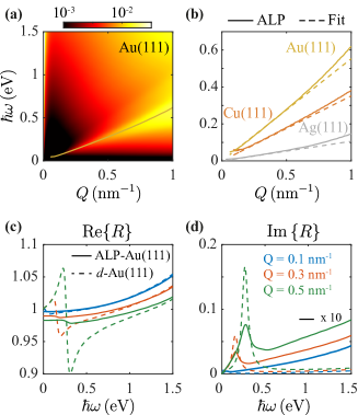
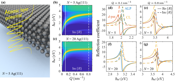
Acoustic surface plasmons due to Shockley surface states. At low frequencies, a feature exhibiting a nearly linear dispersion emerges in the loss function associated with (111)-faceted metal surfaces, indicating the existence of acoustic surface plasmons formed by Shockley surface states 51, 52, 29, 47, 53, 54. Figure 3 shows the loss function of a Au(111) surface, which in the low-frequency regime is marked by the presence of a well-defined but relatively broad feature associated with its acoustic surface plasmon (c.f. scales of Figure 3a and Figure 2a). Next, we present the dispersion relation of acoustic surface plasmons akin to the Au(111), Ag(111), and Cu(111) surfaces obtained within the ALP framework (solid curves), and whose slope—corresponding to the acoustic surface plasmon velocity—is then determined through a linear fit (dashed curves); see Table 2). Note that the intrinsic acoustic surface plasmons supported by noble metal surfaces of well-defined crystallographic orientation have been characterized experimentally under different conditions: For Au(111), a phase velocity was observed at room temperature 55, while a value was reported at K 56; the extracted value in the present work (see Table 2) is close to unity.
| Material | (eV) | (SS) | / | (meV) | |
|---|---|---|---|---|---|
| Ag(111) | 0.026 | 0.40 57 | 1.0690 | 27.5 | |
| Au(111) | 0.525 | 0.26 57 | 0.9971 | 83.7 | |
| Cu(111) | 0.356 | 0.41 57 | 0.9676 | 118.1 |
The Shockley 2DEG supported by the (111)-facets can be accounted for through the Feibelman -parameter (since it can mimic a surface conductivity). We exploit this by introducing, in an ad hoc fashion, a heuristic expression for as described in the Methods section. We emphasize here that, because we account for the 2DEG heuristically, intraband transitions involving surface states are omitted in the ALP-based calculations. Then, in possession of both and , we use eq 2 to reproduce the optical response calculations performed with the ALP model. As observed in Figure 5c-d, where the real and imaginary parts of the reflection coefficient for Au(111) are compared for different values of , the reconstruction is satisfactory for small , although the amplitudes of these already weak features are not well-reproduced.
Nonclassical optical response of ultrathin metal films. The practical utility of the -parameter framework for mesoscale electromagnetism becomes apparent by recognizing that, once obtained for a specific dielectric–metal interface, they can be readily incorporated in a broad range of optical response calculations, either via -parameter-corrected scattering coefficients 35 or through -parameter-modified boundary conditions. 39, 40
As a concrete example, we now investigate the nonclassical optical response of ultrathin silver films comprising (111) atomic monolayers. In Figure 4a-b we present the loss function for ultrathin silver films with thicknesses and , which is dominated by the surface plasmon supported by the films; incidentally, the plasmon dispersion relation obtained from the ALP model closely resembles that obtained in a simple Fabry-Pérot description, even without including -parameters. Figures 4(c-f) compare the spectral dependence of the reflection coefficient for selected in-plane wave vectors predicted in the ALP model with FP models that include or neglect the -parameter correction. Here, we observe an unremarkable effect resulting from for small values of the parallel wave vector ( nm-1), while at larger in-plane momenta, for which the plasmon resonance approaches the plasma frequency (), noticeable differences emerge (e.g., for nm-1). The excellent agreement between the calculated curves based on the -parameter and ALP frameworks underscores how the optical response obtained analytically using eq (4) together with the Feibelman -parameters (c.f. eqs 2–3) accurately accounts for quantum effects impacting the film’s electromagnetic response. In particular, the optical response for extremely-thin Ag films, down to atomic planes, appears to be well-reproduced by the surface-corrected thin film reflection coefficient, although the application of the -parameters to describe such films is questionable.
Graphene next to crystallographically faceted metal films: Acoustic graphene plasmons We consider the extrinsic acoustic plasmons produced by the hybridization of a closely-spaced graphene layer with a crystalline metal film. Unlike the intrinsic acoustic plasmons supported by the (111)-facets, the introduced graphene layer and its opto-electronic tunability provides an additional knob to actively modulate the optical response of the emerging low-energy acoustic plasmon modes with linearized dispersion 58. The experimental capability to position graphene within nm of a noble metal layer is launching explorations of extreme light concentration within the gap region 59, 60, 61, which could be further improved by employing crystalline noble metals 43. In what follows, we summarize the semi-analytical FP description of the optical response based on the extracted -parameters.
For a zero-thickness 2D graphene monolayer, the reflection and transmission coefficients in the quasistatic limit 62 read
where is the nonlocal conductivity of graphene, which we treat here at the level of the nonlocal RPA 63, 36, 64, 65 (using Mermin’s prescription for the relaxation-time approximation which conserves local particle number 66; we take ).
Similarly to eq (4), we compute the reflection coefficient of an extended graphene sheet on top of a semi-infinite metal via the FP resonance model as
| (6) |
where is the spacing between the metal surface and graphene, and and are the reflection and transmission coefficients of graphene. In our calculations we follow the prescription of ref 43 to account for spatial dependence of the carbon 2p orbitals extending outwards from the graphene monolayer plane, leading to the corrected graphene reflection and transmission coefficients and , where nm is the interlayer spacing of graphite and is a coupling factor defined in ref 43. Taking into account the aforementioned effective graphene thickness, the separation distance actually corresponds to the distance between the edge of the graphene and the metal surface, i.e., corresponds to a distance between the graphene center and the metal surface.
Acoustic plasmons are anticipated to emerge even by depositing graphene directly on metallic films 58, heralded by the prominent low-energy linear dispersion feature in the reflection coefficient of Figure 5a. For the considered hybrid graphene–Au(111) surface, the excited extrinsic acoustic plasmons are characterized as before by with denoting the associated group velocity; in such a heterostructure, is determined by graphene Fermi energy and the graphene–metal spacing , as illustrated in Figure 5b. Accordingly, a given dispersion velocity can be obtained by different combinations of and .
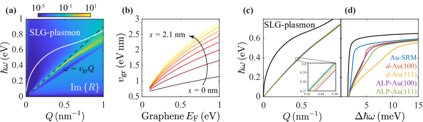
Figure 5c reveals that among Ag, Au, and Cu (not shown), neither the choice of metal nor the considered crystalline facet strongly influences the acoustic plasmon dispersion characteristics; at low energies, these metals are all good conductors that effectively screen the graphene plasmon and render its dispersion acoustic. We remark, however, that, for the same heterostructure, the dispersion relation of the higher energy plasmon mode is indeed dominated by the metal properties 43. However, inspection of the linewidths of the acoustic plasmon in Figure. 5d reveals a substantial dependence on the quantum-mechanical effects arising from the various crystalline facets, which is underlined by the underestimation of spectral widths in the SRM 43. In particular, the obtained results suggest that crystalline Au(111) gives rise to additional surface-enhanced damping when compared to Au(100), presumably due to the presence of a surface state, and warranting further study of the acoustic plasmons supported by heterostructured crystalline metal films.
Crystallographically faceted nanoparticles. Going beyond planar, layered media, we explore the role of crystallographic orientation in faceted noble metal nanoparticles (NPs). The optical response of metallic NPs is dominated by the localized surface plasmon (LSP) resonances supported by it; the most prominent of which are typically those of dipolar character, as they can couple to far-field radiation. As the NP size is reduced towards nanometric dimensions, the ensuing NP’s surface-to-volume ratio grows and leads to more pronounced nonclassical corrections associated with the NP’s quantum surface-response. To illustrate the importance of using the appropriate Feibelman -parameters for determining the quantum surface-response associated with specific facets, we consider in Figure 6 a realistic faceted silver NP. Any natural NP—especially those with characteristic dimensions —no matter how carefully synthesized, will always deviate from a perfect sphere, as a consequence of its growth in a sequence of specific crystallographic planes 67. The shape closest to a sphere is that of a truncated octahedron, as depicted schematically in Figure 6; it is characterized by large hexagonal surfaces and smaller facets.
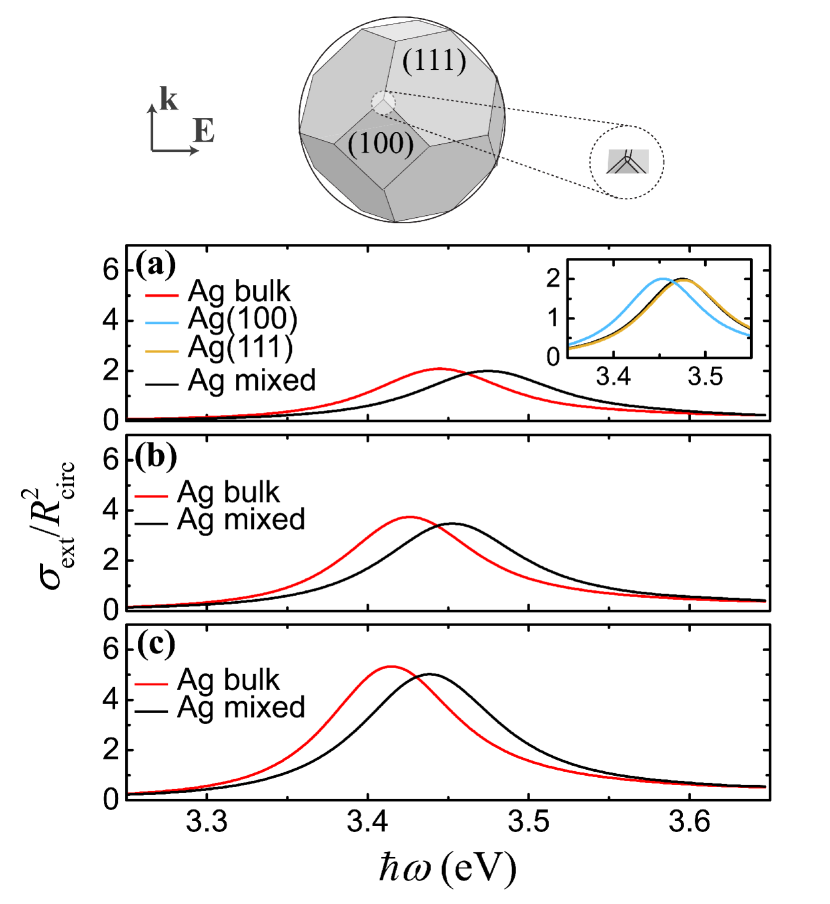
To compute the NP’s nonclassical extinction cross-section , we implement in a finite-element method (FEM) solver the mesoscopic boundary conditions within the Feibelman formalism 39, 40, 35, 36; in practice, this is tantamount to the introduction of surface electric and magnetic currents (see Methods) characterized by the -parameters presented in Figure 1. Comparing with the classical spectra (red curves), it is clear that the effect of the -parameters is to capture the nonlocal optical response of such an NP. As expected for silver, the spectra are shifted to higher energies as a result of an inward shift () of the screening charges. Studying different NP sizes, from to in "radius" (meaning here the circumscribed radius ), a consistent trend is observed, with the resonance broadening (as a result of increased Landau damping) and undergoing stronger blueshifts, as the size decreases, which is compatible with the predictions of nonlocal hydrodynamics 41, 68, 69, and also in accordance with electron energy-loss spectroscopy (EELS) experiments 70, 71, 72, 73. The observed behavior is mainly attributed to the facets, as shown in the inset of Figure 6a, where blue and yellow curves show the corresponding spectra assuming that the entire NP is described solely by the or -parameters, respectively; since the associated surface area of the facets is smaller, and their corresponding Feibelman parameters are significantly lower in magnitude than those of the surface, they only induce a small frequency shift in the spectra. Then, while the main effect is due to the facets, the corresponding spectrum almost coincides with the “mixed” one, where each facet is described by its own parameters. It is also worth noting that, because the truncated octahedron constitutes a highly symmetric shape, the optical response of such NPs resembles that of spheres, and thus changing the angle of incidence is not expected to lead to significant differences.
3 Conclusions
The inherently large losses sustained by noble metals is often regarded as the Achilles heel of nano-optical functionalities based on plasmonics, and has motivated intensive efforts to identify new material platforms that can support long-lived polaritons. Crystalline noble metal films constitute one appealing possibility that is now becoming increasingly available. We have introduced surface response corrections in the form of Feibelman -parameters extracted from quantum-mechanical optical response calculations of crystalline noble metals. As demonstrated here, the tabulated -parameters for gold, silver, and copper surfaces with specific crystallographic orientations can be straightforwardly incorporated in analytical models as well as in computational electromagnetic solvers for the calculation the nonclassical optical response of various nanoplasmonic systems of current interest that contain these facets. We envision that the -parameters reported here can be widely deployed to describe quantum surface effects in crystalline noble metal surfaces which are actively explored for novel nanophotonic functionalities and applications.
4 Methods
4.1 Microscopic surface-response functions: Feibelman d-parameters
The surface-response functions introduced by Feibelman 33, and , are formally given, respectively, by the first-moment of the quantum mechanical induced charge () and of the parallel component of the corresponding current density () 33, 34, 35, 36
| (7a) | ||||
| (7b) | ||||
in the long-wavelength limit. The Feibelman parameters can be rigorously incorporated in electrodynamic problems by appropriately adjusting the boundary conditions at the surface 33, both in analytical treatments 39, 34, 35, 36 and in numerical implementations 39, 40.
It is implicit that in the presence of more mechanisms, and . In the following we separately consider contributions from bulk spatial dispersion—relevant for any metal surface with a compressible electron gas—and Shockley surface states—relevant to the (111) noble-metal surfaces.
4.1.1 Contributions from bulk spatial dispersion
The surface-response functions associated with the spatial dispersion (nonlocal response) of the bulk response functions of the metal, i.e., the wave vector dependence of the dielectric function, can be expressed through the specular reflection model46, 47, 36
| (8a) | ||||
| (8b) | ||||
Note how the vanishing of is a consequence of the charge-neutral interface 37. Below, we discuss how this is changed in the presence of a Shockley surface state.
4.1.2 Contributions from Shockley surface states
We consider the effect of a Shockley surface state, while for simplicity leaving out the response associated with the spatial dispersion of the bulk states. We note that, with our sign convention of the surface-normal, the surface conductivity is related to the Feibelman parameter as 36. Furthermore, in the nonretarded limit, the 2D plasmon dispersion relation associated with is generally given by 36. Anticipating that we have a Shockley surface state that supports an acoustic plasmon 27, corresponding to a dispersion relation , we thus find the connection between this phase velocity and the Feibelman parameters to be:
| (9a) | ||||
| (9b) | ||||
For low frequencies () this simplifies to , while it naturally vanishes at high frequencies. When implemented in the mesoscopic boundary conditions for the electrodynamics, these Feibelman parameters—by construction—support an acoustic plasmon with the desired phase velocity. Considering the poles of the scattering coefficients (see eqs 2 and 3) and substituting in eqs 9, we obtain
| (10) |
and we indeed find two decoupled solutions: the "classical" surface plasmon resonance (defined by ) and the (added ad-hoc) acoustic one with . Table 2 gathers the obtained phase velocities by fitting the acoustic surface plasmon featured in the optical response (see Figure 5a), and the damping by associating it to the width of a Lorentzian; specifically, the widths have been computed numerically from the second derivative of the imaginary part of the reflection coefficient in order to remove the background contribution (see Figure 5d).
4.1.3 Extraction of the -parameters for crystalline metal surfaces
We describe crystalline metal films quantum mechanically, simulating their optical response at the level of the random-phase approximation (RPA) following the procedure of ref 43: As explained therein, metal films are considered to have translational symmetry in the plane, so that their electronic wave functions are amenable to expansion in a plane wave basis according to , with denoting the normalization area, the 2D electron momentum, and the spatial dependence of state in the quantization direction ; the latter quantity is obtained by solving the eigenvalue problem to obtain the associated energy eigenvalues of the 1D Hamiltonian determining the band dispersion . The 1D potential , here referred to as the atomic layer potential (ALP), is selected from those reported in ref 44 that characterize faceted metals of thickness composed of atomic planes stacked in the -direction with inter-layer spacing (naturally, is an integer multiple of ).
Electronic bands are populated by successively filling the lowest bands until the effective bulk electronic density is reached, thereby determining the Fermi energy as
| (11) |
where the sums over terminate when , i.e., is the highest partially-occupied band. The electronic densities are determined by imposing the experimentally-established value of for a given noble metal in the bulk limit (i.e., for a sufficiently thick film). For consistency with experimental observations 74, 75, 76, we impose a linear variation in the effective mass of the parabolic bands as a function of their quantized energies according to , thereby avoiding artifacts due to an unrealistic number of excitation channels for vertical transitions introduced by perfectly-aligned parabolic bands; specific parameters used in our calculations are reported in Table 3—note that the surface states for (111) noble metal facets are assigned specific experimentally-determined effective masses.
We characterize the optical response of noble metal films by the reflection coefficient , expressed as a function of the optical in-plane wave vector and frequency . Considering that the relevant length scales are far smaller than the involved optical wavelengths, we invoke the quasistatic approximation to compute the reflection coefficient in terms of electrostatic potentials as , where is the sum of external and induced potentials, the former exciting the system and the latter obtained as in terms of the film susceptibility , which we compute in the ALP-RPA formalism reported in ref 43. In principle, the RPA response function is constructed by summing over all possible transitions between electronic states; however, because the Shockley surface state of the (111) facet is incorporated in following the ad-hoc prescription of the previous section, the reflection coefficient that is used to extract is computed by excluding intraband transitions involving surface states, thereby avoiding double-counting of the associated 2DEG.
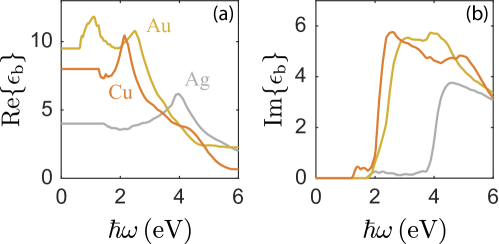
Following the RPA description of ref 43, we correct the Coulomb interaction to incorporate screening from core electrons using the experimentally-extracted polycrystalline dielectric functions parametrized in Table 1 and plotted below in Fig. 7. The associated with a given noble metal facet is extracted from ALP-RPA simulations of a sufficiently thick film, so that the optical response is converged with the number of atomic planes. More specifically, we obtain by fitting eq 2 to the ALP-RPA reflection coefficient of the thick film, employing the corresponding bulk dielectric function of eq 1; importantly, the bulk plasma frequency for each metal facet that enters eq 1 in the fitting is obtained from the ALP-RPA response of a finite film for sufficiently small in-plane wave vector, e.g., , so that nonlocal effects are safely neglected and the surface plasmon resonance ( eV) is captured in an uncorrected Fabry–Pérot description; this procedure enables a stable parametrization of a crystallographic facet’s bulk properties when the contribution from the -parameters is negligible. In practice, the surface plasmon for a finite film with atomic planes appears at lower energies than the surface plasmon for the semi-infinite film, and the associated resonance is undamped by interband transitions, thereby giving rise to a well-defined peak (see, for instance, Figure 4) from which is obtained by fitting , c.f. eq 2 in the limit.
Once the bulk properties for each facet are set, we construct at a given by fitting eq 4 for a given value of to the ALP-RPA response. We maintain a large number of layers to avoid quantum finite size effects emerging in thin films ( atomic layers). We then confirm that convergence is maintained with the calculated as the number of layers and/or parallel wave vector is varied, where the latter condition is typically satisfied for nm-1. After the parameters are obtained, they are applied to thick (Figure 2) and thin films (Figure 4) to confirm their applicability.
In the case of the (100)-facet metals we set , whereas for the (111)-facet the prescription of eq 9 is employed to describe the intrinsic low-energy acoustic plasmon; as anticipated, approaches zero when , and hence such a condition was imposed after solving for .
| Material | ) | (SS) | (eV) | (eV) | (eV) | |||
|---|---|---|---|---|---|---|---|---|
| Ag(100) | -0.0817 | 0.2116 | - | 0.40 77 | 0.8710 | -4.43 44 | 8.80 | 0.021 |
| Ag(111) | -0.1549 | -0.5446 | 0.40 57 | 0.25 52 | 0.8381 | -4.63 78, 79 | 9.19 | 0.021 |
| Au(100) | -0.1068 | -0.1802 | - | 0.24 | 0.9199 | -5.47 80 | 8.67 | 0.071 |
| Au(111) | -0.1660 | -0.8937 | 0.26 57 | 0.26 52 | 0.9443 | -5.50 78, 79 | 9.88 | 0.071 |
| Cu(100) | -0.0751 | 0.1078 | - | 0.34 | 0.9634 | -4.59 80 | 11.38 | 0.103 |
| Cu(111) | -0.1084 | -0.3303 | 0.41 57 | 0.31 52 | 0.9285 | -4.98 80 | 11.50 | 0.103 |
4.2 Finite-element implementation
To calculate the extinction spectra of the truncated octahedra, we used the commercial FEM solver Comsol Multiphysics 5.4. As it has been shown elsewhere 40, 35, 39, Feibelman parameters can be incorporated in any computational method by adjusting the boundary conditions. More specifically, the Feibelman parameters introduce discontinuities in the parallel components of the electric and magnetic fields, which can be expressed through 40, 35, 39
| (12a) | |||
| (12b) |
where , , and are the electric, magnetic, and displacement fields on side of an interface between two media and , and is the unit vector normal to the interface. These conditions can be readily implemented in version 5.4 of Comsol Multiphysics, through surface current and surface magnetic current densities, expressed through the down and up functions in Comsol Multiphysics for the fields at sides 1 and 2. Since the expressions for these currents (right-hand sides of eqs 12a and 12b) contain the fields themselves, the problem needs to be solved iteratively, starting with the currents due to the incident plane wave. To calculate scattering and absorption cross section, we need to integrate the Poynting flux of the scattered and total field over a surface (a sphere) enclosing the NP, with radius large enough ( nm more than ) to ensure that numerical noise due to the currents close to the surface will be minimum. For sharp-edged NPs like the octahedra studied here, it is also necessary to introduce some rounding, to ensure that any spurious edge/corner modes will be absent. This is needed in the classical calculation, in the absence of surface currents; when these are present, the additional damping they introduce smooths things nicely. However, for a direct comparison between the two cases, it is necessary to include the same rounding in both cases. This, however, causes an additional numerical problem, because the iterative method diverges when surface currents are added in such small rounded elements. For this reason, surface currents are only used to describe the square and hexagonal facets. This is in practice not a bad approximation, as one needs to somehow introduce a smooth transition between the two different current densities. In terms of set-up parameters, a cubic physical domain of side nm was used, surrounded by nm-thick perfectly-matched layers. For the finite-element discretization, a mesh of 30000 domain elements with maximum element size nm and minimum element size nm provided converged spectra.
A. R. E. and F. J. G. A. acknowledge support from ERC (Advanced Grant 789104-eNANO), the Spanish MINECO (MAT2017-88492-R and SEV2015-0522), the Catalan CERCA Program, and Fundació Privada Cellex. N. A. M. is a VILLUM Investigator supported by VILLUM FONDEN (grant No. 16498) and Independent Research Fund Denmark (grant no. 7026-00117B). The Center for Nano Optics is financially supported by the University of Southern Denmark (SDU 2020 funding). Simulations were supported by the DeIC National HPC Centre, SDU.
References
- Gramotnev and Bozhevolnyi 2010 Gramotnev, D. K.; Bozhevolnyi, S. I. Plasmonics beyond the diffraction limit. Nat. Photon. 2010, 4, 83–91
- Gramotnev and Bozhevolnyi 2014 Gramotnev, D. K.; Bozhevolnyi, S. I. Nanofocusing of electromagnetic radiation. Nat. Photon. 2014, 8, 14–23
- Fernández-Domínguez et al. 2017 Fernández-Domínguez, A. I.; García-Vidal, F. J.; Martín-Moreno, L. Unrelenting plasmons. Nat. Photon. 2017, 11, 8–10
- Lal et al. 2008 Lal, S.; Clare, S. E.; Halas, N. J. Nanoshell-Enabled Photothermal Cancer Therapy: Impending Clinical Impact. Acc. Chem. Res. 2008, 41, 1842–1851
- Rastinehad et al. 2019 Rastinehad, A. R. et al. Gold nanoshell-localized photothermal ablation of prostate tumors in a clinical pilot device study. Proc. Natl. Acad. Sci. U. S. A. 2019, 116, 18590–18596
- Wang et al. 2012 Wang, P.; Huang, B.; Dai, Y.; Whangbo, M.-H. Plasmonic photocatalysts: harvesting visible light with noble metal nanoparticles. Phys. Chem. Chem. Phys. 2012, 14, 9813–9825
- Zhang et al. 2013 Zhang, X.; Chen, Y. L.; Liu, R.-S.; Tsai, D. P. Plasmonic photocatalysis. Rep. Prog. Phys. 2013, 76, 046401
- Kristensen et al. 2017 Kristensen, A.; Yang, J. K. W.; Bozhevolnyi, S. I.; Link, S.; Nordlander, P.; Halas, N. J.; Mortensen, N. A. Plasmonic colour generation. Nat. Rev. Mater. 2017, 2, 16088
- Atwater and Polman 2010 Atwater, H. A.; Polman, A. Plasmonics for improved photovoltaic devices. Nat. Mater. 2010, 9, 205–213
- Smith et al. 2015 Smith, J. G.; Faucheaux, J. A.; Jain, P. K. Plasmon resonances for solar energy harvesting: a mechanistic outlook. Nano Today 2015, 10, 67–80
- Boltasseva and Atwater 2011 Boltasseva, A.; Atwater, H. A. Low-loss plasmonic metamaterials. Science 2011, 331, 290–291
- Alonso Calafell et al. 2019 Alonso Calafell, I.; Cox, J. D.; Radonjić, M.; Saavedra, J. R. M.; García de Abajo, F. J.; Rozema, L. A.; Walther, P. Quantum computing with graphene plasmons. npj Quantum Inf. 2019, 5, 37
- Fernández-Domínguez et al. 2018 Fernández-Domínguez, A. I.; Bozhevolnyi, S. I.; Mortensen, N. A. Plasmon-Enhanced Generation of Nonclassical Light. ACS Photonics 2018, 5, 3447–3451
- Zhou et al. 2016 Zhou, Z.; Zhao, Z.; Yu, Y.; Ai, B.; Möhwald, H.; Chiechi, R. C.; Yang, J. K. W.; Zhang, G. From 1D to 3D: Tunable Sub-10 nm Gaps in Large Area Devices. Adv. Mater. 2016, 28, 2956–2963
- Baumberg et al. 2019 Baumberg, J. J.; Aizpurua, J.; Mikkelsen, M. H.; Smith, D. R. Extreme nanophotonics from ultrathin metallic gaps. Nat. Mater. 2019, 18, 668–678
- Kossoy et al. 2014 Kossoy, A.; Merk, V.; Simakov, D.; Leosson, K.; Kéna-Cohen, S.; Maier, S. A. Optical and Structural Properties of Ultra-thin Gold Films. Adv. Opt. Mater. 2014, 3, 71–77
- Maniyara et al. 2019 Maniyara, R. A.; Rodrigo, D.; Yu, R.; Canet-Ferrer, J.; Ghosh, D. S.; Yongsunthon, R.; Baker, D. E.; Rezikyan, A.; García de Abajo, F. J.; Pruneri, V. Tunable plasmons in ultrathin metal films. Nat. Photon. 2019, 13, 328–333
- Abd El-Fattah et al. 2019 Abd El-Fattah, Z. M.; Mkhitaryan, V.; Brede, J.; Fernández, L.; Li, C.; Guo, Q.; Ghosh, A.; Rodríguez Echarri, A.; Naveh, D.; Xia, F.; Ortega, J. E.; García de Abajo, F. J. Plasmonics in atomically thin crystalline silver films. ACS Nano 2019, 13, 7771–7779
- Boltasseva and Shalaev 2019 Boltasseva, A.; Shalaev, V. M. Transdimensional Photonics. ACS Photonics 2019, 6, 1–3
- Huang et al. 2010 Huang, J.-S.; Callegari, V.; Geisler, P.; Bruening, C.; Kern, J.; Prangsma, J. C.; Wu, X.; Feichtner, T.; Ziegler, J.; Weinmann, P.; Kamp, M.; Forchel, A.; Biagioni, P.; Sennhauser, U.; Hecht, B. Atomically flat single-crystalline gold nanostructures for plasmonic nanocircuitry. Nat. Commun. 2010, 1, 150
- Hoffmann et al. 2016 Hoffmann, B.; Bashouti, M. Y.; Feichtner, T.; Mačković, M.; Dieker, C.; Salaheldin, A. M.; Richter, P.; Gordan, O. D.; Zahn, D. R. T.; Spiecker, E.; Christiansen, S. New insights into colloidal gold flakes: structural investigation, micro-ellipsometry and thinning procedure towards ultrathin monocrystalline layers. Nanoscale 2016, 8, 4529–4536
- Méjard et al. 2017 Méjard, R.; Verdy, A.; Demichel, O.; Petit, M.; Markey, L.; Herbst, F.; Chassagnon, R.; des Francs, G. C.; Cluzel, B.; Bouhelier, A. Advanced engineering of single-crystal gold nanoantennas. Opt. Mater. Express 2017, 7, 1157–1168
- Cheng et al. 2019 Cheng, F.; Lee, C.-J.; Choi, J.; Wang, C.-Y.; Zhang, Q.; Zhang, H.; Gwo, S.; Chang, W.-H.; Li, X.; Shih, C.-K. Epitaxial Growth of Optically Thick, Single Crystalline Silver Films for Plasmonics. ACS Appl. Mater. Interfaces 2019, 11, 3189–3195
- McPeak et al. 2015 McPeak, K. M.; Jayanti, S. V.; Kress, S. J. P.; Meyer, S.; Iotti, S.; Rossinelli, A.; Norris, D. J. Plasmonic films can easily be better: rules and recipes. ACS Photonics 2015, 2, 326–333
- Inglesfield 1982 Inglesfield, J. E. Surface electronic structure. Rep. Prog. Phys. 1982, 45, 223–284
- Shockley 1939 Shockley, W. On the Surface States Associated with a Periodic Potential. Phys. Rev. 1939, 56, 317–323
- Echenique et al. 2001 Echenique, P. M.; Osma, J.; Machado, M.; Silkin, V. M.; Chulkov, E. V.; Pitarke, J. M. Surface-state electron dynamics in noble metals. Prog. Surf. Sci. 2001, 67, 271–283
- Suto et al. 1989 Suto, S.; Tsuei, K.-D.; Plummer, E. W.; Burstein, E. Surface-plasmon energy and dispersion on Ag single crystals. Phys. Rev. Lett. 1989, 63, 2590–2593
- Diaconescu et al. 2007 Diaconescu, B.; Pohl, K.; Vattuone, L.; Savio, L.; Hofmann, P.; Silkin, V. M.; Pitarke, J. M.; Chulkov, E. V.; Echenique, P. M.; Farías, D.; Rocca, M. Low-energy acoustic plasmons at metal surfaces. Nature 2007, 448, 57–59
- Politano et al. 2015 Politano, A.; Silkin, V. M.; Nechaev, I. A.; Vitiello, M. S.; Viti, L.; Aliev, Z. S.; Babanly, M. B.; Chiarello, G.; Echenique, P. M.; Chulkov, E. V. Interplay of Surface and Dirac Plasmons in Topological Insulators: The Case of Bi2Se3. Phys. Rev. Lett. 2015, 115, 216802
- Varas et al. 2016 Varas, A.; García-González, P.; Feist, J.; García-Vidal, F. J.; Rubio, A. Quantum plasmonics: from jellium models to ab initio calculations. Nanophotonics 2016, 5, 409–426
- Zhu et al. 2016 Zhu, W.; Esteban, R.; Borisov, A. G.; Baumberg, J. J.; Nordlander, P.; Lezec, H. J.; Aizpurua, J.; Crozier, K. B. Quantum mechanical effects in plasmonic structures with subnanometre gaps. Nat. Commun. 2016, 7, 11495
- Feibelman 1982 Feibelman, P. J. Surface electromagnetic fields. Prog. Surf. Sci. 1982, 12, 287–407
- Christensen et al. 2017 Christensen, T.; Yan, W.; Jauho, A.-P.; Soljačić, M.; Mortensen, N. A. Quantum corrections in nanoplasmonics: shape, scale, and material. Phys. Rev. Lett. 2017, 118, 157402
- Gonçalves et al. 2020 Gonçalves, P. A. D.; Christensen, T.; Rivera, N.; Jauho, A.-P.; Mortensen, N. A.; Soljačić, M. Plasmon-Emitter Interactions at the Nanoscale. Nat. Commun. 2020, 11, 366
- Gonçalves 2020 Gonçalves, P. A. D. Plasmonics and Light–Matter Interactions in Two-Dimensional Materials and in Metal Nanostructures: Classical and Quantum Considerations; Springer Nature, 2020
- Liebsch 1997 Liebsch, A. Electronic Excitations at Metal Surfaces; Springer: New York, 1997
- Gonçalves et al. 2020 Gonçalves, P. A. D.; Christensen, T.; Peres, N. M. R.; Jauho, A.-P.; Epstein, I.; Koppens, F. H. L.; Soljačić, M.; Mortensen, N. A. Quantum Surface-Response of Metals Revealed by Acoustic Graphene Plasmons. arXiv:2008.07613 2020,
- Yan et al. 2015 Yan, W.; Wubs, M.; Mortensen, N. A. Projected Dipole Model for Quantum Plasmonics. Phys. Rev. Lett. 2015, 115, 137403
- Yang et al. 2019 Yang, Y.; Zhu, D.; Yan, W.; Agarwal, A.; Zheng, M.; Joannopoulos, J. D.; Lalanne, P.; Christensen, T.; Berggren, K. K.; Soljačić, M. A general theoretical and experimental framework for nanoscale electromagnetism. Nature 2019, 576, 248–252
- García de Abajo 2008 García de Abajo, F. J. Nonlocal effects in the plasmons of strongly interacting nanoparticles, dimers, and waveguides. J. Phys. Chem. C 2008, 112, 17983–17987
- Johnson and Christy 1972 Johnson, P. B.; Christy, R. W. Optical constants of the noble metals. Phys. Rev. B 1972, 6, 4370–4379
- Echarri et al. 2019 Echarri, A. R.; Cox, J. D.; García de Abajo, F. J. Quantum Effects in the Acoustic Plasmons of Atomically-Thin Heterostructures. Optica 2019, 6, 630–641
- Chulkov et al. 1999 Chulkov, E. V.; Silkin, V. M.; Echenique, P. M. Image potential states on metal surfaces: binding energies and wave functions. Surf. Sci. 1999, 437, 330–352
- Ritchie and Marusak 1966 Ritchie, R. H.; Marusak, A. L. The surface plasmon dispersion relation for an electron gas. Surf. Sci. 1966, 4, 234–240
- Ford and Weber 1984 Ford, G. W.; Weber, W. H. Electromagnetic interactions of molecules with metal surfaces. Phys. Rep. 1984, 113, 195–287
- Pitarke et al. 2007 Pitarke, J. M.; Silkin, V. M.; Chulkov, E. V.; Echenique, P. M. Theory of surface plasmons and surface plasmon polaritons. Rep. Prog. Phys. 2007, 70, 1–87
- Rocca et al. 1995 Rocca, M.; Yibing, L.; de Mongeot, F. B.; Valbusa, U. Surface plasmon dispersion and damping on Ag(111). Phys. Rev. B 1995, 52, 14 947–14 953
- Park and Palmer 2009 Park, S. J.; Palmer, R. E. Plasmon dispersion of the Au (111) surface with and without self-assembled monolayers. Phys. Rev. Lett. 2009, 102, 216805
- Robusto and Braunstein 1981 Robusto, P. F.; Braunstein, R. Optical measurements of the surface plasmon of copper. Phys. Status Solidi B 1981, 107, 443–449
- Pitarke et al. 2004 Pitarke, J. M.; Nazarov, V. U.; Silkin, V. M.; Chulkov, E. V.; Zaremba, E.; Echenique, P. M. Theory of acoustic surface plasmons. Phys. Rev. B 2004, 70, 205403
- Silkin et al. 2005 Silkin, V. M.; Pitarke, J. M.; Chulkov, E. V.; Echenique, P. M. Acoustic surface plasmons in the noble metals Cu, Ag, and Au. Phys. Rev. B 2005, 72, 115435
- Pohl et al. 2010 Pohl, K.; Diaconescu, B.; Vercelli, G.; Vattuone, L.; Silkin, V. M.; Chulkov, E. V.; Echenique, P. M.; Rocca, M. Acoustic surface plasmon on Cu(111). EPL (Europhysics Letters) 2010, 90, 57006
- Yan et al. 2012 Yan, J.; Jacobsen, K. W.; Thygesen, K. S. Conventional and acoustic surface plasmons on noble metal surfaces: A time-dependent density functional theory study. Phys. Rev. B 2012, 86, 241404
- Park and Palmer 2010 Park, S. J.; Palmer, R. E. Acoustic plasmon on the Au (111) surface. Phys. Rev. Lett. 2010, 105, 016801
- Vattuone et al. 2013 Vattuone, L.; Smerieri, M.; Langer, T.; Tegenkamp, C.; Pfnür, H.; Silkin, V. M.; Chulkov, E. V.; Echenique, P. M.; Rocca, M. Correlated motion of electrons on the Au (111) surface: anomalous acoustic surface-plasmon dispersion and single-particle excitations. Phys. Rev. Lett. 2013, 110, 127405
- Reinert et al. 2001 Reinert, F.; Nicolay, G.; Schmidt, S.; Ehm, D.; Hüfner, S. Direct measurements of the L-gap surface states on the (111) face of noble metals by photoelectron spectroscopy. Phys. Rev. B 2001, 63, 115415
- Principi et al. 2018 Principi, A.; van Loon, E.; Polini, M.; Katsnelson, M. I. Confining graphene plasmons to the ultimate limit. Phys. Rev. B 2018, 98, 035427
- Alcaraz Iranzo et al. 2018 Alcaraz Iranzo, D.; Nanot, S.; Dias, E. J. C.; Epstein, I.; Peng, C.; Efetov, D. K.; Lundeberg, M. B.; Parret, R.; Osmond, J.; Hong, J.-Y.; Kong, J.; Englund, D. R.; Peres, N. M. R.; Koppens, F. H. L. Probing the ultimate plasmon confinement limits with a van der Waals heterostructure. Science 2018, 360, 291–295
- Lee et al. 2019 Lee, I.-H.; Yoo, D.; Avouris, P.; Low, T.; Oh, S.-H. Graphene acoustic plasmon resonator for ultrasensitive infrared spectroscopy. Nat. Nanotechnol. 2019, 14, 313––319
- Epstein et al. 2020 Epstein, I.; Alcaraz, D.; Huang, Z.; Pusapati, V.-V.; Hugonin, J.-P.; Kumar, A.; Deputy, X. M.; Khodkov, T.; Rappoport, T. G.; Hong, J.-Y.; Peres, N. M. R.; Kong, J.; Smith, D. R.; Koppens, F. H. L. Far-field excitation of single graphene plasmon cavities with ultracompressed mode volumes. Science 2020, 368, 1219–1223
- García de Abajo 2014 García de Abajo, F. J. Graphene Plasmonics: Challenges and Opportunities. ACS Photonics 2014, 1, 135–152
- Gonçalves and Peres 2016 Gonçalves, P. A. D.; Peres, N. M. R. An Introduction to Graphene Plasmonics, 1st ed.; World Scientific: Singapore, 2016
- Wunsch et al. 2006 Wunsch, B.; Stauber, T.; Sols, F.; Guinea, F. Dynamical Polarization of Graphene at Finite Doping. New J. Phys. 2006, 8, 318
- Hwang and Sarma 2007 Hwang, E. H.; Sarma, S. D. Dielectric function, screening, and plasmons in two-dimensional graphene. Phys. Rev. B 2007, 75, 205418
- Mermin 1970 Mermin, N. D. Lindhard dielectric function in the relaxation-time approximation. Phys. Rev. B 1970, 1, 2362–2363
- Myroshnychenko et al. 2008 Myroshnychenko, V.; Carbó-Argibay, E.; Pastoriza-Santos, I.; Pérez-Juste, J.; Liz-Marzán, L. M.; García de Abajo, F. J. Modeling the Optical Response of Highly Faceted Metal Nanoparticles with a Fully 3D Boundary Element Method. Adv. Mater. 2008, 20, 4288–4293
- Mortensen et al. 2014 Mortensen, N. A.; Raza, S.; Wubs, M.; Søndergaard, T.; Bozhevolnyi, S. I. A generalized nonlocal optical response theory for plasmonic nanostructures. Nat. Commun. 2014, 5, 3809
- Raza et al. 2015 Raza, S.; Bozhevolnyi, S. I.; Wubs, M.; Mortensen, N. A. Nonlocal optical response in metallic nanostructures. J. Phys.: Condens. Matter 2015, 27, 183204
- Ouyang et al. 1992 Ouyang, F.; Batson, P. E.; Isaacson, M. Quantum size effects in the surface-plasmon excitation of small metallic particles by electron-energy-loss spectroscopy. Phys. Rev. B 1992, 46, 15421–15425
- Scholl et al. 2012 Scholl, J. A.; Koh, A. L.; Dionne, J. A. Quantum plasmon resonances of individual metallic nanoparticles. Nature 2012, 483, 421
- Raza et al. 2013 Raza, S.; Stenger, N.; Kadkhodazadeh, S.; Fischer, S. V.; Kostesha, N.; Jauho, A.-P.; Burrows, A.; Wubs, M.; Mortensen, N. A. Blueshift of the surface plasmon resonance in silver nanoparticles studied with EELS. Nanophotonics 2013, 2, 131–138
- Raza et al. 2015 Raza, S.; Kadkhodazadeh, S.; Christensen, T.; Di Vece, M.; Wubs, M.; Mortensen, N. A.; Stenger, N. Multipole plasmons and their disappearance in few-nanometer silver nanoparticles. Nat. Commun. 2015, 6, 8788
- Mueller et al. 1990 Mueller, M. A.; Miller, T.; Chiang, T.-C. Determination of the bulk band structure of Ag in Ag/Cu (111) quantum-well systems. Phys. Rev. B 1990, 41, 5214
- Matsuda et al. 2004 Matsuda, I.; Tanikawa, T.; Hasegawa, S.; Yeom, H. W.; Tono, K.; Ohta, T. Quantum-Well States in Ultra-Thin Metal Films on Semiconductor Surfaces. e-J. Surf. Sci. Nanotechnol. 2004, 2, 169–177
- Becker et al. 2006 Becker, M.; Crampin, S.; Berndt, R. Theoretical analysis of STM-derived lifetimes of excitations in the Shockley surface-state band of Ag (111). Phys. Rev. B 2006, 73, 081402
- García-Lekue et al. 2003 García-Lekue, A.; Pitarke, J. M.; Chulkov, E. V.; Liebsch, A.; Echenique, P. M. Role of occupied bands in the dynamics of excited electrons and holes in Ag. Phys. Rev. B 2003, 68, 045103
- Kevan and Gaylord 1987 Kevan, S. D.; Gaylord, R. H. High-resolution photoemission study of the electronic structure of the noble-metal (111) surfaces. Phys. Rev. B 1987, 36, 5809
- Paniago et al. 1995 Paniago, R.; Matzdorf, R.; Meister, G.; Goldmann, A. Temperature dependence of Shockley-type surface energy bands on Cu (111), Ag (111) and Au (111). Surf. Sci. 1995, 336, 113–122
- Michaelson 1977 Michaelson, H. B. The work function of the elements and its periodicity. J. Appl. Phys. 1977, 48, 4729–4733