Infrared study of the multiband low-energy excitations of the topological antiferromagnet MnBi2Te4
Abstract
With infrared spectroscopy we studied the bulk electronic properties of the topological antiferromagnet MnBi2Te4 with . With the support of band structure calculations, we assign the intra- and interband excitations and determine the band gap of 0.17 eV. We also obtain evidence for two types of conduction bands with light and very heavy carriers. The multiband free carrier response gives rise to an unusually strong increase of the combined plasma frequency, , below 300 K. The band reconstruction below , yields an additional increase of and a splitting of the transition between the two conduction bands by about 54 meV. Our study thus reveals a complex and strongly temperature dependent multi-band low-energy response that has important implications for the study of the surface states and device applications.
The focus in the research on topological quantum materials Hasan and Kane (2010); Qi and Zhang (2011); Haldane (2017); Tokura et al. (2019) has recently moved on to systems with magnetic order which enable a variety of field-controlled quantum states Wan et al. (2011); Yu et al. (2010); Chang et al. (2013, 2015); Qi et al. (2008); Essin et al. (2009); Mong et al. (2010); Xiao et al. (2018); He et al. (2017), like the quantum anomalous Hall (QAH) effect Yu et al. (2010); Chang et al. (2013, 2015), the topological axion state Qi et al. (2008); Essin et al. (2009); Mong et al. (2010); Xiao et al. (2018), and Majorana fermions He et al. (2017); Qi and Zhang (2011). Such materials have been obtained, e.g. by creating heterostructures from magnetic and topological materials or by adding magnetic defects to topological materials. With the latter approach, the QAH effect has been realized for the first time in Cr-doped (Bi,Sb)2Te3 films Chang et al. (2013). The ideal candidates, however, are bulk topological materials with intrinsic magnetic order for which various problems inherent to thin film growth and defect engineering can be avoided.
A promising candidate is MnBi2Te4 (MBT) which is a topological insulator with A-type antiferromagnetic (AFM) order as predicted by theory Otrokov et al. (2019a); Li et al. (2019a); Zhang et al. (2019); Li et al. (2019b) and recently confirmed by experiements Otrokov et al. (2019b); Zeugner et al. (2019); Vidal et al. (2019); Lee et al. (2019); Yan et al. (2019a); Cui et al. (2019); Gong et al. (2019); Yan et al. (2019b); Deng et al. (2020); Liu et al. (2020); Ge et al. (2020); Hu et al. (2020); Wu et al. (2019); Chen et al. (2019a). Notably, the bulk AFM transition at 25 K has been predicted to strongly affect the electronic states at the (0001) surface, since it creates a gap on the Dirac cone Otrokov et al. (2019a); Li et al. (2019a); Zhang et al. (2019); Otrokov et al. (2019b). Moreover, for thin films the topological properties should depend on the number of MBT layers such that an axion insulator or a QAH insulator appears for even and odd numbers, respectively Otrokov et al. (2019a); Li et al. (2019a). A quantized Hall conductance has indeed been observed in few layer MBT films Deng et al. (2020); Liu et al. (2020); Ge et al. (2020), albeit only in magnetic fields of 5 – 10 Tesla that change the magnetic order to a ferromagnetic one Liu et al. (2020); Ge et al. (2020). The properties of the surface of MBT single crystals are also debated. For example, the formation of a gap below of the Dirac cone at the (0001) surface is seen in some angle-resolved photoemission spectroscopy (ARPES) studies Otrokov et al. (2019b); Zeugner et al. (2019); Vidal et al. (2019); Lee et al. (2019) but not in others Nevola et al. ; Hao et al. (2019); Chen et al. (2019b); Swatek et al. (2020); Li et al. (2019c). This calls for further studies of the surface structural and magnetic properties Hao et al. (2019). Likewise, the bulk-like low energy excitations and their modification in the AFM state remain to be fully understood.
Here we study the bulk electronic properties of MnBi2Te4 crystals with infrared (IR) spectroscopy. In combination with band-structure calculations, we assign the intra- and interband excitations and estimate the inverted bulk band gap and the chemical potential. We also study the excitations of the free carriers and determine their plasma frequency. The latter has a surprisingly low value and an unusual dependence, with a pronounced anomaly below . We show that this anomalous behavior can be explained in terms of two conduction bands with largely different effective masses. Below we also identify a splitting of the transitions between the light and heavy conduction bands (by about 54 meV) that arises from the magnetic coupling between the conduction electrns and the localized Mn moments and agrees with the one seen with ARPES Chen et al. (2019b); Swatek et al. (2020); Li et al. (2019c); Estyunin et al. (2020). This information about the multiband nature of the free carriers and their low-energy excitations is a prerequisite for understanding the plasmonic properties in the bulk as well as of the surface states and their eventual device applications. In the first place, it calls for attempts to reduce the defect concentration and thus the -type doping such that a simpler single band picture applies.
Two batches of MBT single crystals were grown with a flux method Chen et al. (2019a) at Sun Yat-Sen University (Sample A) and Beijing Institute of Technology (Sample B). Both have a metallic in-plane resistivity with an anomaly around K, as shown in Fig. 1(a) for sample A. The negative Hall-resistivity of sample A in Fig. 1(b) indicates electron-like carriers with a concentration of , in agreement with most previous studies Lee et al. (2019); Yan et al. (2019a); Cui et al. (2019); Chen et al. (2019c); Li et al. (2020). Details about the IR reflectivity measurements and the Kramers-Kronig analysis are given in section A of the supplemental material (SM).
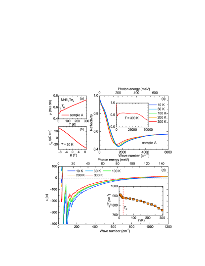
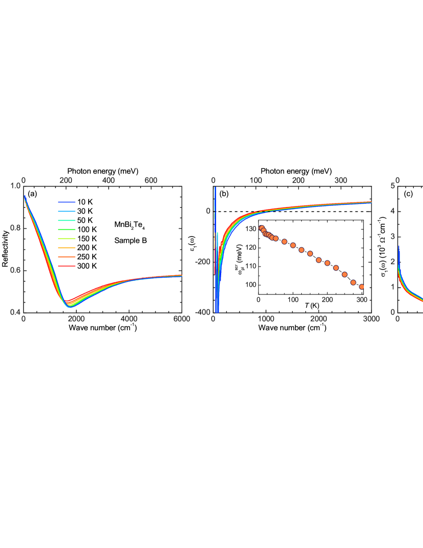
Figure 1(c) shows for sample A the temperature () dependent reflectivity up to 6 000. The inset shows the room temperature spectrum up to 50 000. Below about 1 500 there is a sharp upturn of toward unity that is characteristic of a plasma edge due to the itinerant carriers. This plasma edge shifts to higher frequency as the decreases, indicating an enhancement of free carrier density, , or a reduction of effective mass, . Very similar spectra have been obtained for sample B (see section B in the SM), the following discussion is therefore focused on sample A.
Fig. 1(d) displays the dependence of the real part of the dielectric function . The spectra reveal an inductive behavior with a downturn of toward negative values at low frequency that is another hallmark of a metallic response. The sharp features at 47, 84 and 133 are IR-active phonons that are not further discussed here. The horizontal dashed line shows the zero crossing of , which marks the screened plasma frequency , where is the high-frequency dielectric constant and is the free carrier plasma frequency. The inset details the dependence of which reveals an unusually large increase from about 750 at 300 K to 880 at 30 K. There is also a sudden, additional increase below to about 910 at 10 K which provides a first spectroscopic indication that the AFM order has a pronounced effect on the electronic properties.
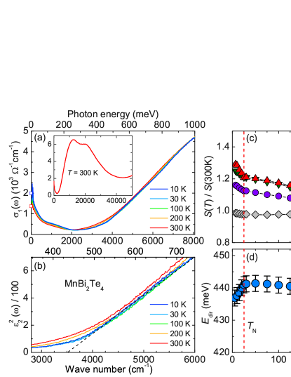
Figure 2(a) displays the dependence of the real part of the optical conductivity up to 8 000. The inset shows the 300 K spectrum up to 50 000 which is dominated by two interband transitions with bands around 12 500 and 20 000, in agreement with Ref. Jahangirli et al. (2019). The optical response below 8 000 consists of a Drude peak with a tail extending to about 2 000 that is well separated from the onset of strong interband transitions above 3 000. The Drude peak grows upon cooling, consistent with the increase of in Fig. 1(d). The conductivity data at 10 and 300 K from Fig. 1(a) (squares on the -axis) agree with the zero-frequency extrapolation of . The width of the Drude peak of about 500 is nearly independent and much larger than e.g. in Bi2Te3 Dordevic et al. (2013). The scattering thus seems to be dominated by disorder effects e.g. due to Mn-Bi antisite defects Zeugner et al. (2019). The dependence of the onset of the strong interband transitions, , that are most likely direct transitions across the band gap, , between the valence band (VB) and the conduction band (CB), has been obtained with a linear extrapolation of , as shown in Fig. 2(b). It increases toward low , but decreases suddenly below [see Fig. 2(d)].
The spectral changes have been further analyzed by calculating the evolution of the spectral weight (SW), , for different cut-off frequencies . Figure 2(c) shows the dependence of the ratio at representative cut-offs. At 500 and 2 000, where the free carrier response dominates, the SW increases towards low and exhibits an additional upturn below , in agreement with the trend of in Fig. 1(d). At the higher cutoffs, this increase becomes less pronounced until at 8 000 (1 eV) it is almost constant. This confirms that the SW redistribution is confined to energies below 1 eV.
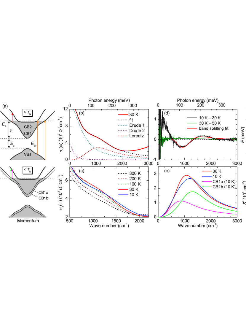
Next, we analyze in more detail the response below 2 000 which contains besides the Drude response a weak band due to a low-energy interband transition. This is evident in Fig. 3(b) which displays the spectrum at 30 K together with a Drude-Lorentz fit. It reveals a band centered around 1 100 that overlaps with the tail of the Drude response. The fit function contains two Drude-terms with different plasma frequencies and scattering rates of , and , , respectively. The band at 1 100 is described by a Lorenz function. Details about the Drude-Lorentz analysis are given in section C of the SM.
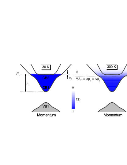
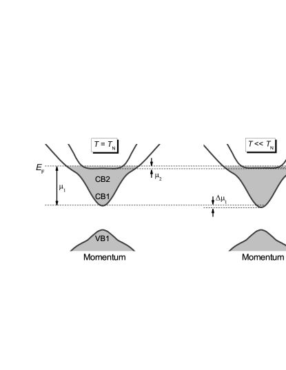
Fig. 3(a) shows a schematics of the band structure in the vicinity of the chemical potential that is consistent with our optical data, with our band calculations along the –Y direction (see setion E in the SM) and also with reported ARPES data Chen et al. (2019b); Swatek et al. (2020); Hao et al. (2019). In addition to a pair of conduction and valence bands that is forming an inverted band gap (CB1 and VB1), it contains a second conduction band (CB2) that is located slightly above CB1 and has a very flat bottom and thus a very large effective mass. As shown in the following, our optical data suggest that the chemical potential, , is crossing both CB1 and CB2 (at low temperature). This assignment is consistent with the use of two Drude-peaks in fitting the low-energy response in the previous paragraph. It also accounts for the weak band around 1 100 in terms of the interband transitions between CB1 and CB2 (red arrow). The optical excitations at higher energy involve transitions across the direct band gap , from the VB to the empty states in CB1 and CB2, as illustrated in Fig. 3(a) by the orange arrows. Note that if would not be crossing CB2, the transition between the top of VB1 and the bottom of CB2, which are both rather flat and optically allowed, would give rise to a strong peak near that is clearly not seen in the spectra of Fig. 2(a). On the other hand, a pronounced peak around 3 350 (415 meV) has been observed in the corresponding spectra which were taken on the as grown surface of the same sample (see section D in the SM). This implies that for the as grown surface the chemical potential is somewhat lower, such that it falls below CB2. Such a reduction of the free carrier concentration might be caused, for example, by the localization of carries on extrinsic defects or by a lower concentration of intrinsic defects that are responsible for the -type doping.
With this band assignment, we can estimate for the cleaved MBT surfaces the low- value of the chemical potential by using the expressions , with the Fermi-vector , the carrier density , and the spin and band degeneracies and Zhang et al. (2019); Li et al. (2019a); Tang et al. (2016). Using and (see section C in the SM), as well as and according to the band structure calculations (see section E in the SM), we derive eV and eV for CB1 and CB2, respectively. Accordingly, with an estimate of 0.415 eV for the direct interband transition between VB1 and CB2 around the point, we derive a band gap of eV at 30 K (as explained in section F of the SM, the largest uncertainty arises from the estimate of ), which agrees well with the reported values from band calculations and ARPES Li et al. (2019a); Zhang et al. (2019); Li et al. (2019b); Otrokov et al. (2019b); Zeugner et al. (2019); Vidal et al. (2019); Lee et al. (2019); Hao et al. (2019); Chen et al. (2019b); Swatek et al. (2020).
Next, we focus on the band reconstruction below , especially on the anomalous changes of the interband transition at 1 100 which provide evidence for a magnetic splitting of CB1. In the paramagnetic state the spectra in Fig. 3(c) exhibit a monotonic increase in this frequency range that arises mainly from the growth of the Drude SW, as shown in Figs. 1(d) and 2(c). Below , this trend is suddenly interrupted, i.e. decreases from about 500 to 1 200 whereas it gets anomalously enhanced between 1 200 and 2 000. These anomalous changes, that are detailed in Fig. 3(d) in terms of the difference spectrum of at 30 and 10 K, are characteristic of a splitting of the conduction band CB1 into CB1a and CB1b, as indicated in the lower panel of Fig. 3(a). This band splitting, which is caused by the exchange interaction of the conduction electrons with the Mn moments which lifts the band degeneracy due to the unit cell doubling in the AFM state, is also seen in recent ARPES studies Chen et al. (2019b); Swatek et al. (2020); Estyunin et al. (2020); Li et al. (2019c). Note that the magnetic splitting of CB2 is assumed to be much smaller and thus is neglected. This assumption is supported by ARPES data Chen et al. (2019b); Swatek et al. (2020); Estyunin et al. (2020); Li et al. (2019c), and also by the comparison of the density of states at the Fermi-level derived from our optical data with the Korringa-slope of the ESR data in Ref. Otrokov et al. (2019b), as outlined in section H of the SM. The red line in Fig. 3(d) confirms that the spectral changes below arise from a corresponding splitting of the interband transitions from CB1a to CB2 and CB1b to CB2. It has been obtained with the function: , for which represents the Lorentz function and the subscripts and denote the interband transitions from the split bands, for which we assume , and . The parameters in the paramagnetic state have been obtained from a Drude-Lorentz fit at 30 K. The contribution of the individual bands CB1a and CB1b are shown in Fig. 3(e). The red line in Fig. 3(d) shows that this band splitting model allows us to reproduce the -shaped feature of . An additional contribution that arises from a much weaker and almost featureless dependent change of the background, that occurs also above , has been corrected using the difference between 30 and 50 K (olive line). The full dependence of and below is displayed in Fig. 3(f). It shows that the band splitting amounts to 54 meV at 10 K and is almost symmetric with respect to the band position at 30 K. Fig. 3(g) displays the corresponding spectral weights and which exhibit a weak anisotropy that is consistent with the band splitting model. Note that the splitting of CB1 also accounts for the anomalous decrease of below , since it reduces .
Finally, we return to the unusually large increase of towards low and its pronounced anomaly below . The 20% increase between 300 and 30 K can hardly arise from a volume contraction effect that would imply a giant expansion coefficient of . Likewise, the anomalous increase of below would require unrealistically large magneto-striction effects. Instead, we propose that the strong increase of toward low results from an exchange of conduction electrons between the light and very heavy states in CB1 and CB2 Drabble (1958); Goldsmid (1958); Chand et al. (1984); Carter and Bate (1970); Wieting and Schlüter (1979). Due to their largely different effective masses, the distribution of electrons is strongly dependent on the relative position of CB1 and CB2 with respect to the chemical potential. Accordingly, the dependence of the chemical potential accounts for the observed change of in the paramagnetic state (see section F in the SM). The anomalous increase of below requires in addition a small shift of the center of CB1a and CB1b against CB2 of 10 meV (see section G in the SM). Note that the corresponding effect of the magnetic slitting of CB1a and CB1b is weaker and of the opposite sign (see section G in the SM).
At last, we mention that for the majority of degenerate doped narrow gap semiconductors exhibits a much weaker dependence and usually decreases upon cooling due to the freeze-out of carriers. Interestingly, another rare exception, for which exhibits a similarly strong increase toward low , is Bi2Te3. While the samples studied in Ref. Thomas et al. (1992) where hole doped, in analogy to MBT, they may also have light and very heavy valence electrons.
In summary, we determined the bulk, optical properties of the AFM topological insulator MnBi2Te4. In combination with band structure calculations, we assigned the intra- and interband excitations and obtained a bulk band gap of 0.17 eV. We also provided evidence for two conduction bands with largely different effective masses of 0.12 and 3 and chemical potentials of 0.266 and 0.019 eV (at 30 K). A dependent transfer of electrons between these conduction bands and the subsequent change of the average effective mass, can account for an unusually strong dependence of the free carrier plasma frequency, . Below 25 K, we observed clear signs of a band reconstruction in terms of an additional, anomalous increase of and a splitting of the transition between the conduction bands. This detailed information about the bulk band structure and the multi-band charge carrier response is a prerequisite for the understanding of the plasmonic properties of the bulk and surface states and their device applications.
Acknowledgements.
We acknowledge discussion with A. Akrap, G. Khalliulin and Z. Rukelj. The work in Fribourg was supported by the Schweizerische Nationalfonds (SNF) by Grant No. 200020-172611. V.K. acknowledges support by the Deutsche Forschungsgemeinschaft (DFG) through Grant No. KA1694/12-1. N.M. acknowledges the support of the Science Development Foundation under the President of the Republic of Azerbaijan (Grant No. EİF-BGM-4-RFTF-1/2017-21/04/1-M-02). The work at Beijing was supported by the Natural Science Foundation of China (NSFC Grant No. 11734003), the National Key R&D Program of China (Grant No.2016YFA0300600), the Beijing Natural Science Foundation(Grant No. Z190006). Z.W. acknowledges the support from Beijing Institute of Technology Research Fund Program for Young Scholars. B.S. acknowledges the support of the Fundamental Research Funds for the Central Universities, Grant No. 19lgpy260. E.V.C. acknowledges Saint Petersburg State University (Grant No. ID 51126254).Appendix A A: Reflectivity measurement, Kramers-Kronig analysis, and Hall resistivity data
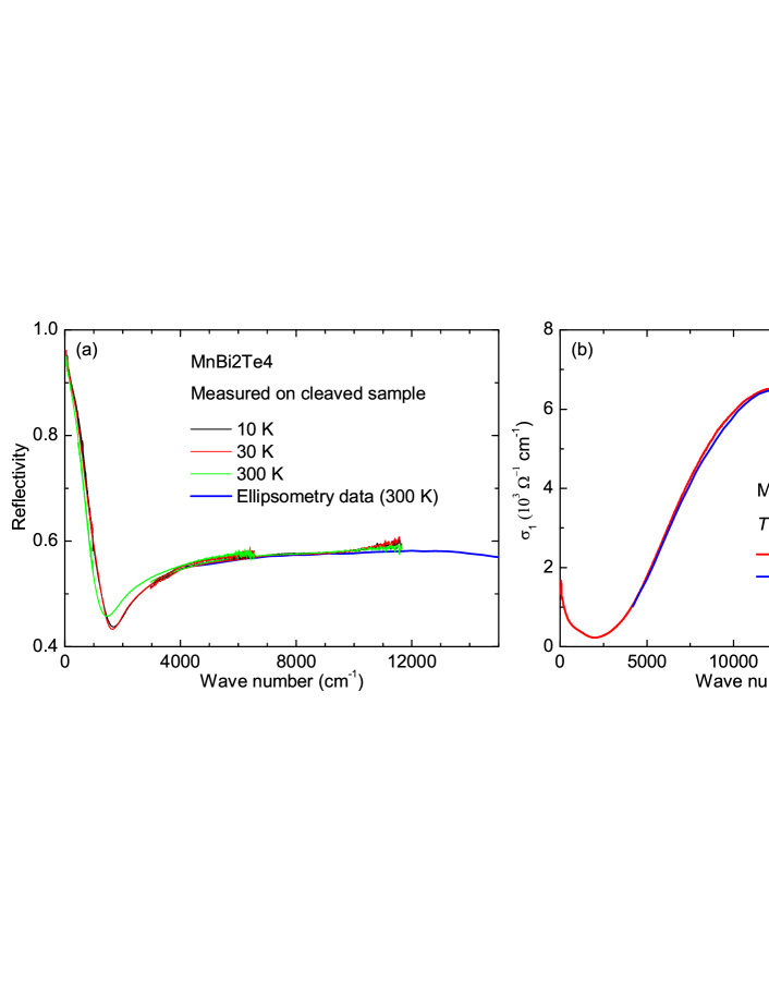
The in-plane reflectivity of MnBi2Te4 was measured at a near-normal angle of incidence using a Bruker VERTEX 70v Fourier transform infrared spectrometer. An in situ gold overfilling technique Homes et al. (1993) was used to obtain the absolute reflectivity. As shown in Figure S1(a), the reflectivity spectra have been measured over a very broad frequency range from 30 to 12 000 on a freshly cleaved sample surface by using a series of combinations of sources, beamsplitters and detectors. The reflectivity spectra at different temperatures from 300 to 7 K were collected with an ARS-Helitran cryostat. Figure S1(a) also shows the raw spectra measured for different frequency ranges at 10, 30 and 300 K. It is evident that all spectra exhibit the same temperature dependence and are overlapping very well in the region where the spectra have been connected to perform the Kramers-Kronig analysis. This confirms the accuracy and reproducibility of the measured reflectivity spectra.
The optical conductivity was obtained from a Kramers-Kronig analysis of Dressel and Grüner (2002). For the low-frequency extrapolation we used a Hagen-Rubens function . On the high-frequency side, the ellipsometry data were used, for which the spectrum in the near-infrared to ultraviolet range (4 000 – 50 000) was measured at room temperature with a commercial ellipsometer (Woollam VASE), and the Kramers-Kronig analysis was anchored by the room temperature ellipsometry data, as shown by the spectra in Figure S1(b).
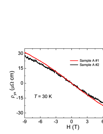
In Fig. S2, we show the Hall resistivity data for MnBi2Te4 at 30 K that were taken on two different pieces of sample A from the same growth batch. Both samples exhibit a negative Hall resistivity with a linear slope from which we obtain conduction electron densities of and , respectively. This confirms that the Hall-effect data are quite reproducible and accurate.
Appendix B B: Optical data of MnBi2Te4 collected on Sample B
The optical data of MnBi2Te4 sample B were measured under the same conditions as reported for sample A in the main text. Fig. S3 shows the temperature dependent optical data in the terms of the reflectivity [Fig. S3(a)], the real part of the dielectric function [Fig. S3(b)], and the real part of the conductivity [Fig. S3(c)]. The optical spectra are very similar to those of sample A as reported in the main text, further confirming the reproducibility and reliability of the measured spectra.
Appendix C C: Drude-Lorentz analysis
We performed a quantitative analysis of the low-energy part of the spectra of sample A by fitting with the following Drude-Lorentz model.
| (1) |
where is the vacuum impedance. The first term with a sum of two Drude terms describes the response of the itinerant carriers in the two conduction bands CB1 and CB2, each characterized by a plasma frequency and a scattering rate . The second term denotes a Lorentz oscillator with the resonance frequency , line width and oscillator strength , that accounts for the interband transitions between CB1 and CB2.
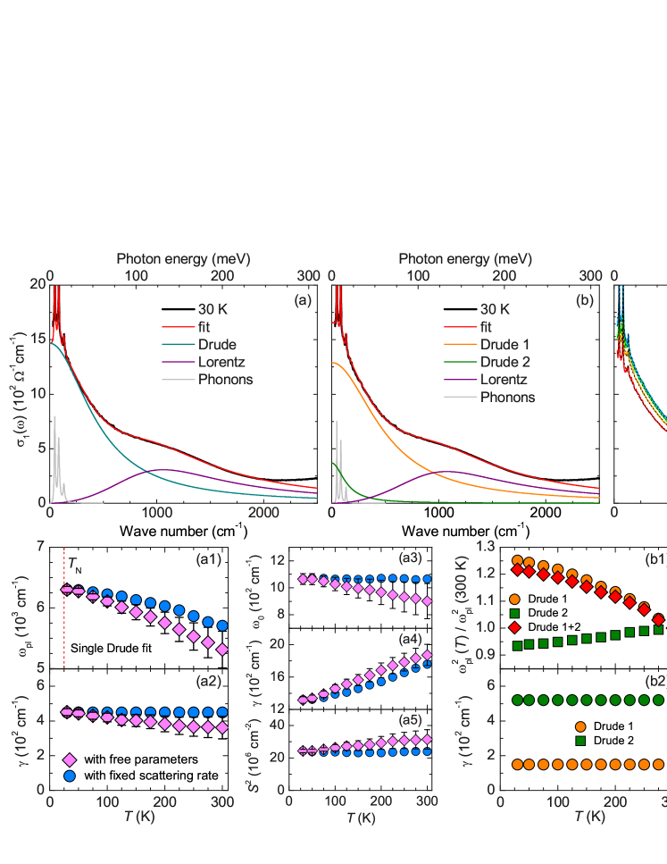
In a first attempt, trying to reduce the fitting parameters, we used a single Drude band and the Lorentz band. Figures S4(a) shows the corresponding Drude-Lorentz fit (red line) to the low-energy part of the spectrum at at 30 K (black curve). Also shown are the contributions of the Drude term (cyan line) and the Lorentz term (purple line) due to the free carriers and the low energy interband transition. An additional contribution from infrared active phonons is shown by the gray line. The obtained plasma frequency and scattering rate at 30 K are and , respectively. Using the squared plasma frequencies, , as a measure of the ratio of the free carrier density , and the effective mass and with , as obtained from the Hall data at 30 K, we derive an effective mass of the conduction electrons of . Such a large value of the effective mass disagrees with the band structure calculations in section E which predict a much smaller effective mass of the lowest conduction band CB1 of . As discussed in the main text, this discrepancy can be resolved by taking into account an additional contribution from the second conduction band CB2 that has very heavy carriers with .
To account for the presence of the two conduction bands CB1 and CB2, we have fitted the spectra with the function in equation (1) using two Drude-terms. Figure S4(b) shows that the two-Drude-model fit (red line) to the spectrum at 30 K (black line) yields a better description in very low energy range than the single-Drude fit in Figure S4(a). As is also described in the main text, the obtained parameters of the two Drude terms are , and , , for CB1 and CB2, respectively. With taken from the Hall-data and the combined plasma frequency of CB1 and CB2, , where and according to the band structure calculations in section E, we derive the carrier concentrations of and for CB1 and CB2, respectively. Alternatively, with the partial plasma frequency and , we obtain and for CB1 and CB2, respectively, and thus . The good agreement of both estimates confirms the self-consistency of our fitting approach with two Drude bands from two conduction bands with light and very heavy electrons, the effective mass from band calculations, and the carrier concentration from the Hall data.
Next, we discuss the dependence of the obtained fit parameters in the paramagnetic state above for the single-Drude as well as the two-Drude models. Figs. S4(a1–a5) show the dependence of the fit parameters for the single Drude model. It yields a nearly independent scattering rate that is also evident from the nearly equal width of the spectra in Fig. S4(c). Accordingly, to reduce the number of fit parameters and to avoid a mixing of spectral weight as the width of the latter increases toward high , we have fitted the dependent spectra with a fixed scattering rate as obtained at 30 K. Figures S4(b1–b5) show the corresponding dependent fit parameters as obtained with the two-Drude model where again the scattering rates have been fixed to the value at 30 K. Figure S4(b1) shows the dependence of the normalized Drude weights . As described in the main text, the total Drude weight increases towards low and grows by about 20% between 300 and 30 K. Notably, the partial Drude weights of CB1 and CB2 exhibit opposite dependent trends, i.e. whereas the Drude weight of CB1 increases toward the one of CB2 decreases. This behavior is consistent with our interpretation, as described in the main text and in section F, that electrons are transferred from CB2 to CB1 as is reduced.
Appendix D D: Additional peak around 3 350in the spectra on the as-grown surface
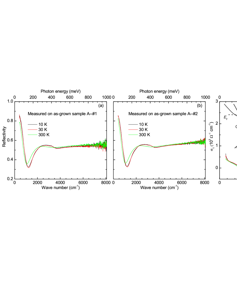
Figures S5(a) and S5(b) show the raw spectra measured in the mid-infrared range on an as-grown surface for two different pieces of sample A. In both cases we observe a strong additional peak around 3 350 that does not show up in the corresponding spectra taken on cleaved surfaces of the same sample A. This peak has been reproduced on several as grown surfaces and apparently is intrinsic to the sample properties rather than just an artefact or a dirt effect. Figure S5(c) shows the corresponding optical conductivity at the as grown surface that has been obtained from a preliminary Kramers-Kronig analysis using the reflectivity data that cover only a limited frequency range. It reveals a pronounced peak peak around 3 350. This additional peak can be naturally explained, as shown by the sketch in the inset of Fig. S5(c), if the Fermi level at the as-grown surface is slightly reduced as compared to the one of the cleaved surface, such that it is located below CB2. In this case, the interband transitions between the top of VB1 and the bottom of CB2 are allowed and yield a pronounced peak since both bands are rather flat giving rise to a high joint density of states. In the future, this assignment could be confirmed with optical studies on cleaved surface of samples with a much lower carrier concentration than for our samples A and B.
Appendix E E: Effective mass from band structure calculations and band degeneracy
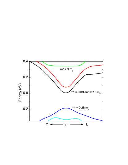
As shown in Fig. S6, the calculations of the band structure (details are described in Ref. Jahangirli et al. (2019)) in the AFM state yield two “split-type” light electron conduction bands with electron effective masses of 0.09 and 0.15 for the lower (black) and upper one (red), respectively. In the paramagnetic state these two bands are degenerate and therefore described in the manuscript as a single band with an average effective mass of 0.12 (CB1). Note that this double degeneracy () is a consequence of the combined inversion and time-reversal symmetry ( symmetry) as described in Ref. Zhang et al. (2019); Li et al. (2019a); Tang et al. (2016) and applies to all bands in the paramagnetic state. The splitting of CB1 in the AFM state, into a lower band with 0.09 (CB1b) and an upper one with 0.15 (CB1a), which is predicted to amount to approximately 80 meV, is a consequence of the broken symmetry that arises from the exchange interaction of the conduction electrons with the localized Mn spins for which the unit cell in the A-type AFM state is doubled along the c-axis. This magnetic interaction thus lifts the band degeneracy () but maintains the spin degeneracy () of CB1a and CB1b. There is also a third band of heavy electrons with very small dispersion and a very large effective mass around 3 that is denoted in the main test as CB2. Since the exchange interaction of its carriers with the localized Mn moments is assumed to be very weak we describe it even in the AFM state in terms of a single band with and . Finally, the estimate of the hole mass of the valence band is about 0.28 .
Effective masses of electrons and holes were estimated by fitting parabola to the calculated dispersion of the electron bands around the point in the directions –Y and –L of the Brillouin zone of MnBi2Te4. Note that the –Y direction lies exactly in the layer plane, as is required to account for the optical transitions in the experimental data for which the polarization vector of the incident light is parallel to the layer plane (perpendicular to the -axis) of the MBT crystal.
Appendix F F: Multi-band approach to describe the dependent redistribution of electrons from CB2 to CB1
The density of states of the conduction electrons of an -type doped three dimensional material is given by
| (2) |
where is the conduction band edge. At finite temperature the Fermi-Dirac distribution is given by
| (3) |
where = ( 0 K) is the Fermi energy and the chemical potential. Accordingly, the carrier density at finite temperature is given by
| (4) |
With the definitions and , this integral can be rewritten in the normalized form:
| (5) |
where the “effective” density of states in the conduction band is
| (6) |
and is known as the Fermi-Dirac integral of order 1/2 (referring to the in the numerator).
For the two conduction bands of MnBi2Te4, CB1 and CB2, the total carrier density at finite temperature thus can be written as:
| (7) |
with
| (8) |
and
| (9) |
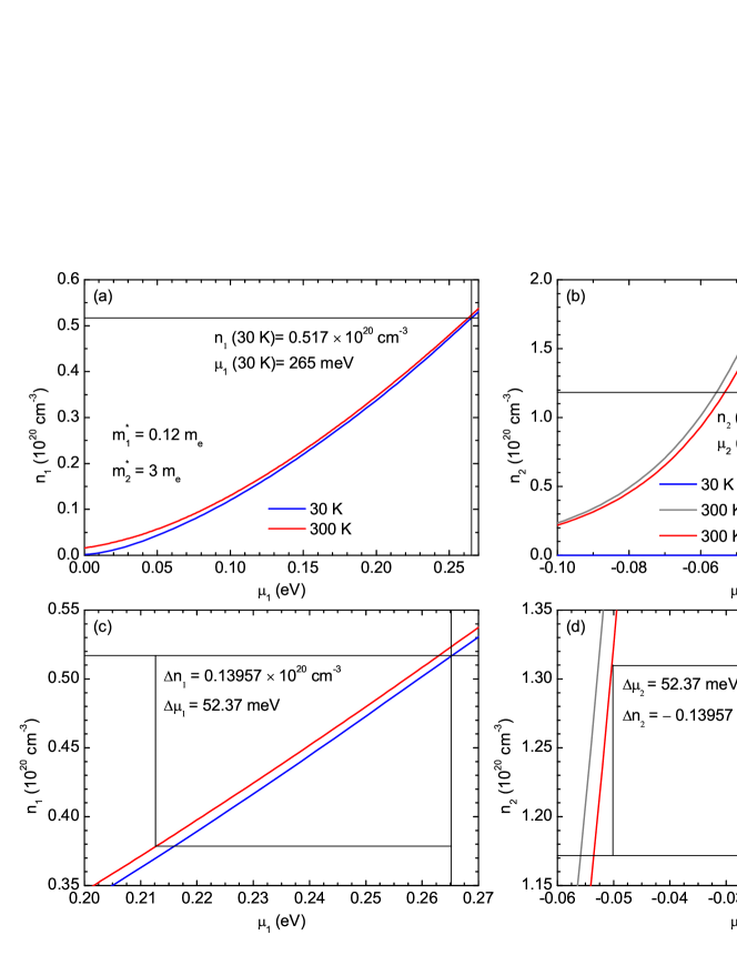
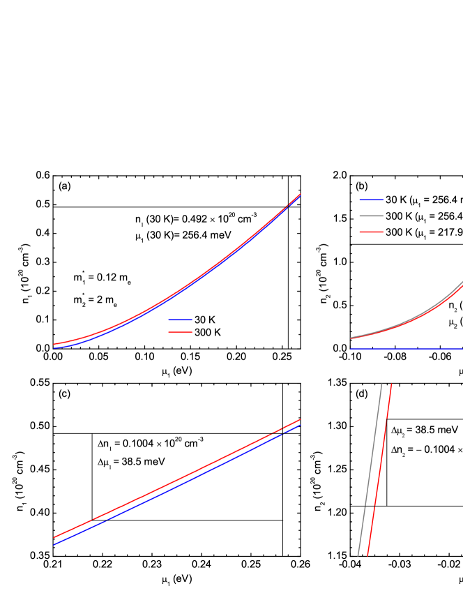
By substituting and into Eq. (8), as shown in Fig. S8(a), we can plot the carrier density of CB1 at 30 and 300 K as a function of (). In section C, we have obtained the carrier density of CB1 at 30 K of . By using the value , we can determine meV.
Note that in Eq. (9) defines the relative position of CB2 with respect to CB1. Since in MnBi2Te4 there is a splitting of CB1 below K, in the following calculations we use as the relative position of CB2 and CB1.
Similarly, by substituting , , and meV into Eq. (9), we can plot the carrier density of CB2 at 30 K as a function of , as shown by the blue line in Fig. S8(b). Furthermore, by using obtained in section C, we can determine meV. As shown in Fig. S8(a) and Fig. S8(b), it is clear that the thermal broadening of the Fermi-edge has a much stronger influence for the states in CB2 than for the ones in CB1. As sketched in Fig. S7, upon increasing the temperature (), the thermal broadening will give rise to a shift of the chemical potential , according to
| (10) |
and
| (11) |
For the measured temperature range between 30 and 300 K, this yields
| (12) |
By substituting , , meV, and meV into Eq. (12), we obtain meV, and thus meV, meV, and . Figure S8(c) and Figure S8(d) show the full temperature dependence of the shift of the chemical potential and the subsequent redistribution of carriers between CB1 and CB2. Accordingly, we obtain the ratio of the corresponding free carrier plasma frequencies of
| (13) |
By substituting , , , and into Eq. (13), we thus obtain
| (14) |
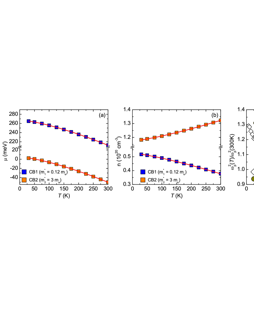
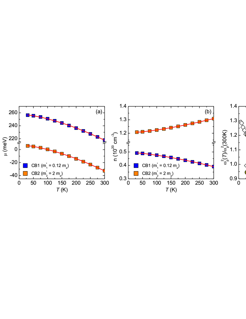
The full temperature dependence of the chemical potentials, the carrier densities and the ratio is displayed in Fig. S9.
These calculations show that the increase of toward low , with a ratio between 30 and 300 K of , can be readily explained in terms of a redistribution of electrons from CB2 to CB1 that arises from sharpening of the Fermi-function and the related increase of the chemical potential by meV. Note that such a shift of the chemical potential (above ) is consistent with the dependence of as shown in Fig. 2(d) in the main text. The calculated value of the increase of the ratio of the squared plasma frequency is even somewhat larger (by about 10%) than the one seen in the experiment. The agreement can still be considered as very good, given the simplicity of the two band model used in the calculations which does not take into account the anti-crossing of CB1 and CB2 imposed by the crystal symmetry that is evident in the band calculations Zhang et al. (2019); Li et al. (2019a) and also shown in the schematics in Fig. S7. It is also possible that the value of the effective mass of the carriers at the bottom of CB2 has been somewhat overestimated. For such a flat band, it can indeed be expected that the parabolic fitting procedure discussed in section E has a sizeable error bar. As shown in Fig. S10 and Fig. S11, we can obtain an excellent agreement between the experimental and the calculated values of the dependent increase of the plasma frequency if we reduce the effective mass of CB2 to a value of . Assuming a value of , instead of , would of course also affect the values of the other calculated parameters. The recalculation, using the relationships and at 30 K and the input parameters and , yields values , , meV, meV, meV between 30 and 300 K. These are still consistent with our experimental data.
Finally, we remark that at high temperature, although the chemical potential falls slightly below CB2, the states near the bottom of CB2 are still occupied with a high probability due to the thermal broadening of the Fermi-function. It is thus not expected that the interband transitions from the top of VB1 to the bottom of CB2 gives rise to a strong peak in the optical conductivity. The experimental data exhibit indeed only a gradual increase of in the relevant frequency range around 3500.
Appendix G G: Redistribution of electrons between CB1 and CB2 below
With respect to the changes below , the thermal effects described in section F yield a 2% increase of that is considerably smaller than the 7% increase in the experimental data and can also not reproduce the sudden slope change around .
As outlined below, the anomalous increase of below can be explained in terms of a small increase of the separation between CB1 and CB2.
To simplify the modeling, we neglect the thermal effects and use here the equations at 0 K. With a parabolic band approximation for and the carrier density , we derive or . For , , , and , we obtained meV and meV.
As sketched in Fig. S12, for a small increase of the separation between CB1 and CB2 from to , the chemical potentials of CB1 and CB2 are changing from and at to and at . Note that the splitting of CB1 below (into CB1a and CB1b) is not considered here. The resulting transfer of carriers from CB2 to CB1 is estimated according to:
| (15) |
To explain an additional 5% increase of below the ratio of the plasma frequencies must be
| (16) |
By substituting 266 meV, , 19 meV, and into equations (15) and (16), we thus obtain 10 meV and 0.3 meV, respectively. Accordingly, the required increase of the separation between CB1 and CB2 below amounts to 10 meV.
At least, we consider the effect of the splitting of CB1 (into CB1a and CB1b) below which turns out to be too small and of the wrong sign to explain the experimental trend.
The carrier concentration of CB1 in the paramagnetic state is taken as
| (17) |
and in the AFM state (with the exchange splitting into CB1a and CB1b) as
| (18) |
By substituting 0.266 eV, , , eV, eV, and , we get . Assuming a constant carrier concentration of CB1 in the paramagnetic and AFM states, i.e. , this gives rise to a slight increase of the Fermi-level . In the presence of CB2, which has a much larger effective mass and thus higher density of states at the Fermi-level, such an increase of the Fermi-level will be counteracted by a redistribution of electrons from CB1 to CB2 according to, . By substituting 0.266 eV, , , eV, eV, 0.019 eV, and , we get 0.15 meV and . Since the total plasma frequency is dominated by the much lighter electrons of CB1, the above described effect would give rise to a 3% decrease of below , as opposed to the observed anomalous increase of below .
Appendix H H: Comparison with electron spin resonance (ESR) data on MnBi2Te4
The Korringa slope of the relaxation rate in the paramagnetic state of electron spin resonance (ESR) measurements is defined as Korringa (1950); Barnes (1981)
| (19) |
where eV/K, eV/G and (for the Mn2+ ion), is the exchange coupling constant between the spins of the localized Mn and the conduction electrons, and is the density of states of the conduction electrons at the Fermi level. The magnitude of thus can be estimated using the values of and as obtained from the ESR and optical data,
| (20) |
can be deduced according to
| (21) |
using the values of the effective mass, and as obtained from the optical data and the unit cell volume taken from Ref. Zeugner et al. (2019). In addition, we have to account for the difference in the carrier concentrations (as determined from the Hall-effect) of the crystals on which the ESR and optics experiments have been performed. For the crystal A of the optics experiment we obtained , and 0.266 eV, 0.019 eV. Considering the spin- and band degeneracy and , respectively, of CB1 and CB2 we thus obtain 0.19 states/eV/fu (formula unit) and 6.47 states/eV/fu for CB1 and CB2, respectively. Taking into account the lower carrier concentration of cm-3 Otrokov et al. (2019b), as compared to cm-3 of our optics crystal A, and using the relationship , we estimate that the Fermi-level of the ESR sample crosses CB1 at eV, whereas CB2 remains above the Fermi-level (and thus empty). Note that this estimate agrees with the ARPES data of the ESR sample that are shown in Ref. Otrokov et al. (2019b). With , we thus obtain 0.15 states/eV/fu. The ESR experiment reported in Ref. Otrokov et al. (2019b), revealed a Korringa-relation with a linear slope of the relaxation rate of G/K for axis and G/K for axis, respectively. Accordingly, we derive values of 70 and 120 meV, respectively, that are of the same order of magnitude as the band splitting between CB1a and CB1b in our optical data of 54 meV. This reasonable agreement, given the uncertainties due to the rather large difference in the carrier concentrations of the samples studied with ESR and optics and the experimental error bars of the various measured parameters, confirms our interpretation of the optical data in terms of an exchange splitting of CB1 that is much larger than the one of CB2 (which has been neglected in the main text). The much weaker exchange coupling of the electrons in CB2 with the Mn spins can also explain that despite the rather different concentration of conduction electrons the various MBT samples have very similar values of Yan et al. (2019a); Cui et al. (2019); Lee et al. (2019); Otrokov et al. (2019b); Chen et al. (2019c); Li et al. (2020), since the former changes in carrier concentration mainly affect the occupation of CB2.
References
- Hasan and Kane (2010) M. Z. Hasan and C. L. Kane, Rev. Mod. Phys. 82, 3045 (2010).
- Qi and Zhang (2011) X.-L. Qi and S.-C. Zhang, Rev. Mod. Phys. 83, 1057 (2011).
- Haldane (2017) F. D. M. Haldane, Rev. Mod. Phys. 89, 040502 (2017).
- Tokura et al. (2019) Y. Tokura, K. Yasuda, and A. Tsukazaki, Nat. Rev. Phys. 1, 126 (2019).
- Wan et al. (2011) X. Wan, A. M. Turner, A. Vishwanath, and S. Y. Savrasov, Phys. Rev. B 83, 205101 (2011).
- Yu et al. (2010) R. Yu, W. Zhang, H.-J. Zhang, S.-C. Zhang, X. Dai, and Z. Fang, Science 329, 61 (2010).
- Chang et al. (2013) C.-Z. Chang, J. Zhang, X. Feng, J. Shen, Z. Zhang, M. Guo, K. Li, Y. Ou, P. Wei, L.-L. Wang, Z.-Q. Ji, Y. Feng, S. Ji, X. Chen, J. Jia, X. Dai, Z. Fang, S.-C. Zhang, K. He, Y. Wang, L. Lu, X.-C. Ma, and Q.-K. Xue, Science 340, 167 (2013).
- Chang et al. (2015) C.-Z. Chang, W. Zhao, D. Y. Kim, H. Zhang, B. A. Assaf, D. Heiman, S.-C. Zhang, C. Liu, M. H. W. Chan, and J. S. Moodera, Nat. Mater. 14, 473 (2015).
- Qi et al. (2008) X.-L. Qi, T. L. Hughes, and S.-C. Zhang, Phys. Rev. B 78, 195424 (2008).
- Essin et al. (2009) A. M. Essin, J. E. Moore, and D. Vanderbilt, Phys. Rev. Lett. 102, 146805 (2009).
- Mong et al. (2010) R. S. K. Mong, A. M. Essin, and J. E. Moore, Phys. Rev. B 81, 245209 (2010).
- Xiao et al. (2018) D. Xiao, J. Jiang, J.-H. Shin, W. Wang, F. Wang, Y.-F. Zhao, C. Liu, W. Wu, M. H. W. Chan, N. Samarth, and C.-Z. Chang, Phys. Rev. Lett. 120, 056801 (2018).
- He et al. (2017) Q. L. He, L. Pan, A. L. Stern, E. C. Burks, X. Che, G. Yin, J. Wang, B. Lian, Q. Zhou, E. S. Choi, K. Murata, X. Kou, Z. Chen, T. Nie, Q. Shao, Y. Fan, S.-C. Zhang, K. Liu, J. Xia, and K. L. Wang, Science 357, 294 (2017).
- Otrokov et al. (2019a) M. M. Otrokov, I. P. Rusinov, M. Blanco-Rey, M. Hoffmann, A. Y. Vyazovskaya, S. V. Eremeev, A. Ernst, P. M. Echenique, A. Arnau, and E. V. Chulkov, Phys. Rev. Lett. 122, 107202 (2019a).
- Li et al. (2019a) J. Li, Y. Li, S. Du, Z. Wang, B.-L. Gu, S.-C. Zhang, K. He, W. Duan, and Y. Xu, Sci. Adv. 5, eaaw5685 (2019a).
- Zhang et al. (2019) D. Zhang, M. Shi, T. Zhu, D. Xing, H. Zhang, and J. Wang, Phys. Rev. Lett. 122, 206401 (2019).
- Li et al. (2019b) J. Li, C. Wang, Z. Zhang, B.-L. Gu, W. Duan, and Y. Xu, Phys. Rev. B 100, 121103 (2019b).
- Otrokov et al. (2019b) M. M. Otrokov, I. I. Klimovskikh, H. Bentmann, D. Estyunin, A. Zeugner, Z. S. Aliev, S. Gaß, A. U. B. Wolter, A. V. Koroleva, A. M. Shikin, M. Blanco-Rey, M. Hoffmann, I. P. Rusinov, A. Y. Vyazovskaya, S. V. Eremeev, Y. M. Koroteev, V. M. Kuznetsov, F. Freyse, J. Sánchez-Barriga, I. R. Amiraslanov, M. B. Babanly, N. T. Mamedov, N. A. Abdullayev, V. N. Zverev, A. Alfonsov, V. Kataev, B. Büchner, E. F. Schwier, S. Kumar, A. Kimura, L. Petaccia, G. Di Santo, R. C. Vidal, S. Schatz, K. Kißner, M. Ünzelmann, C. H. Min, S. Moser, T. R. F. Peixoto, F. Reinert, A. Ernst, P. M. Echenique, A. Isaeva, and E. V. Chulkov, Nature 576, 416 (2019b).
- Zeugner et al. (2019) A. Zeugner, F. Nietschke, A. U. B. Wolter, S. Gaß, R. C. Vidal, T. R. F. Peixoto, D. Pohl, C. Damm, A. Lubk, R. Hentrich, S. K. Moser, C. Fornari, C. H. Min, S. Schatz, K. Kißner, M. Ünzelmann, M. Kaiser, F. Scaravaggi, B. Rellinghaus, K. Nielsch, C. Hess, B. Büchner, F. Reinert, H. Bentmann, O. Oeckler, T. Doert, M. Ruck, and A. Isaeva, Chem. Mater. 31, 2795 (2019).
- Vidal et al. (2019) R. C. Vidal, H. Bentmann, T. R. F. Peixoto, A. Zeugner, S. Moser, C.-H. Min, S. Schatz, K. Kißner, M. Ünzelmann, C. I. Fornari, H. B. Vasili, M. Valvidares, K. Sakamoto, D. Mondal, J. Fujii, I. Vobornik, S. Jung, C. Cacho, T. K. Kim, R. J. Koch, C. Jozwiak, A. Bostwick, J. D. Denlinger, E. Rotenberg, J. Buck, M. Hoesch, F. Diekmann, S. Rohlf, M. Kalläne, K. Rossnagel, M. M. Otrokov, E. V. Chulkov, M. Ruck, A. Isaeva, and F. Reinert, Phys. Rev. B 100, 121104 (2019).
- Lee et al. (2019) S. H. Lee, Y. Zhu, Y. Wang, L. Miao, T. Pillsbury, H. Yi, S. Kempinger, J. Hu, C. A. Heikes, P. Quarterman, W. Ratcliff, J. A. Borchers, H. Zhang, X. Ke, D. Graf, N. Alem, C.-Z. Chang, N. Samarth, and Z. Mao, Phys. Rev. Research 1, 012011 (2019).
- Yan et al. (2019a) J.-Q. Yan, Q. Zhang, T. Heitmann, Z. Huang, K. Y. Chen, J.-G. Cheng, W. Wu, D. Vaknin, B. C. Sales, and R. J. McQueeney, Phys. Rev. Materials 3, 064202 (2019a).
- Cui et al. (2019) J. Cui, M. Shi, H. Wang, F. Yu, T. Wu, X. Luo, J. Ying, and X. Chen, Phys. Rev. B 99, 155125 (2019).
- Gong et al. (2019) Y. Gong, J. Guo, J. Li, K. Zhu, M. Liao, X. Liu, Q. Zhang, L. Gu, L. Tang, X. Feng, D. Zhang, W. Li, C. Song, L. Wang, P. Yu, X. Chen, Y. Wang, H. Yao, W. Duan, Y. Xu, S.-C. Zhang, X. Ma, Q.-K. Xue, and K. He, Chinese Phys. Lett. 36, 076801 (2019).
- Yan et al. (2019b) J.-Q. Yan, S. Okamoto, M. A. McGuire, A. F. May, R. J. McQueeney, and B. C. Sales, Phys. Rev. B 100, 104409 (2019b).
- Deng et al. (2020) Y. Deng, Y. Yu, M. Z. Shi, Z. Guo, Z. Xu, J. Wang, X. H. Chen, and Y. Zhang, Science 367, 895 (2020).
- Liu et al. (2020) C. Liu, Y. Wang, H. Li, Y. Wu, Y. Li, J. Li, K. He, Y. Xu, J. Zhang, and Y. Wang, Nat. Mater. 19, 522 (2020).
- Ge et al. (2020) J. Ge, Y. Liu, J. Li, H. Li, T. Luo, Y. Wu, Y. Xu, and J. Wang, Natl. Sci. Rev. 7, 1280 (2020).
- Hu et al. (2020) C. Hu, K. N. Gordon, P. Liu, J. Liu, X. Zhou, P. Hao, D. Narayan, E. Emmanouilidou, H. Sun, Y. Liu, H. Brawer, A. P. Ramirez, L. Ding, H. Cao, Q. Liu, D. Dessau, and N. Ni, Nat. Commun. 11, 97 (2020).
- Wu et al. (2019) J. Wu, F. Liu, M. Sasase, K. Ienaga, Y. Obata, R. Yukawa, K. Horiba, H. Kumigashira, S. Okuma, T. Inoshita, and H. Hosono, Sci. Adv. 5, eaax9989 (2019).
- Chen et al. (2019a) B. Chen, F. Fei, D. Zhang, B. Zhang, W. Liu, S. Zhang, P. Wang, B. Wei, Y. Zhang, Z. Zuo, J. Guo, Q. Liu, Z. Wang, X. Wu, J. Zong, X. Xie, W. Chen, Z. Sun, S. Wang, Y. Zhang, M. Zhang, X. Wang, F. Song, H. Zhang, D. Shen, and B. Wang, Nat. Commun. 10, 4469 (2019a).
- (32) D. Nevola, H. X. Li, J. Q. Yan, R. G. Moore, H. N. Lee, H. Miao, and P. D. Johnson, “Coexistence of Surface Ferromagnetism and Gapless Topological State in MnBi2Te4,” arXiv:2004.06895(2020) .
- Hao et al. (2019) Y.-J. Hao, P. Liu, Y. Feng, X.-M. Ma, E. F. Schwier, M. Arita, S. Kumar, C. Hu, R. Lu, M. Zeng, Y. Wang, Z. Hao, H.-Y. Sun, K. Zhang, J. Mei, N. Ni, L. Wu, K. Shimada, C. Chen, Q. Liu, and C. Liu, Phys. Rev. X 9, 041038 (2019).
- Chen et al. (2019b) Y. J. Chen, L. X. Xu, J. H. Li, Y. W. Li, H. Y. Wang, C. F. Zhang, H. Li, Y. Wu, A. J. Liang, C. Chen, S. W. Jung, C. Cacho, Y. H. Mao, S. Liu, M. X. Wang, Y. F. Guo, Y. Xu, Z. K. Liu, L. X. Yang, and Y. L. Chen, Phys. Rev. X 9, 041040 (2019b).
- Swatek et al. (2020) P. Swatek, Y. Wu, L.-L. Wang, K. Lee, B. Schrunk, J. Yan, and A. Kaminski, Phys. Rev. B 101, 161109 (2020).
- Li et al. (2019c) H. Li, S.-Y. Gao, S.-F. Duan, Y.-F. Xu, K.-J. Zhu, S.-J. Tian, J.-C. Gao, W.-H. Fan, Z.-C. Rao, J.-R. Huang, J.-J. Li, D.-Y. Yan, Z.-T. Liu, W.-L. Liu, Y.-B. Huang, Y.-L. Li, Y. Liu, G.-B. Zhang, P. Zhang, T. Kondo, S. Shin, H.-C. Lei, Y.-G. Shi, W.-T. Zhang, H.-M. Weng, T. Qian, and H. Ding, Phys. Rev. X 9, 041039 (2019c).
- Estyunin et al. (2020) D. A. Estyunin, I. I. Klimovskikh, A. M. Shikin, E. F. Schwier, M. M. Otrokov, A. Kimura, S. Kumar, S. O. Filnov, Z. S. Aliev, M. B. Babanly, and E. V. Chulkov, APL Mater. 8, 021105 (2020).
- Chen et al. (2019c) K. Y. Chen, B. S. Wang, J.-Q. Yan, D. S. Parker, J.-S. Zhou, Y. Uwatoko, and J.-G. Cheng, Phys. Rev. Materials 3, 094201 (2019c).
- Li et al. (2020) H. Li, S. Liu, C. Liu, J. Zhang, Y. Xu, R. Yu, Y. Wu, Y. Zhang, and S. Fan, Phys. Chem. Chem. Phys. 22, 556 (2020).
- Jahangirli et al. (2019) Z. A. Jahangirli, E. H. Alizade, Z. S. Aliev, M. M. Otrokov, N. A. Ismayilova, S. N. Mammadov, I. R. Amiraslanov, N. T. Mamedov, G. S. Orudjev, M. B. Babanly, A. M. Shikin, and E. V. Chulkov, Journal of Vacuum Science & Technology B 37, 062910 (2019).
- Dordevic et al. (2013) S. V. Dordevic, M. S. Wolf, N. Stojilovic, H. Lei, and C. Petrovic, Journal of Physics: Condensed Matter 25, 075501 (2013).
- Tang et al. (2016) P. Tang, Q. Zhou, G. Xu, and S.-C. Zhang, Nat. Phys. 12, 1100 (2016).
- Drabble (1958) J. R. Drabble, Proc. Phys. Soc. 72, 380 (1958).
- Goldsmid (1958) H. J. Goldsmid, Proc. Phys. Soc. 71, 633 (1958).
- Chand et al. (1984) N. Chand, T. Henderson, J. Klem, W. T. Masselink, R. Fischer, Y.-C. Chang, and H. Morkoĉ, Phys. Rev. B 30, 4481 (1984).
- Carter and Bate (1970) D. Carter and R. Bate, The Physics of Semimetals and Narrow-gap Semiconductors: Proceedings, Supplement to the Journal of physics and chemistry of solids (Pergamon Press, 1970).
- Wieting and Schlüter (1979) T. J. Wieting and M. Schlüter, eds., Electrons and Phonons in Layered Crystal Structures (Springer Netherlands, Dordrecht, 1979).
- Thomas et al. (1992) G. A. Thomas, D. H. Rapkine, R. B. Van Dover, L. F. Mattheiss, W. A. Sunder, L. F. Schneemeyer, and J. V. Waszczak, Phys. Rev. B 46, 1553 (1992).
- Homes et al. (1993) C. C. Homes, M. Reedyk, D. A. Cradles, and T. Timusk, Appl. Opt. 32, 2976 (1993).
- Dressel and Grüner (2002) M. Dressel and G. Grüner, Electrodynamics of Solids (Cambridge University press, 2002).
- Korringa (1950) J. Korringa, Physica 16, 601 (1950).
- Barnes (1981) S. Barnes, Adv. Phys. 30, 801 (1981).