IEEEexample:BSTcontrol
FlexWatts: A Power- and Workload- Aware Hybrid Power Delivery Network for Energy- Efficient Microprocessors
Abstract
Modern client processors typically use one of three commonly-used power delivery network (PDN) architectures: 1) motherboard voltage regulators (MBVR), 2) integrated voltage regulators (IVR), and 3) low dropout voltage regulators (LDO). We observe that the energy-efficiency of each of these PDNs varies with the processor power (e.g., thermal design power (TDP) and dynamic power-state) and workload characteristics (e.g., workload type and computational intensity). This leads to energy-inefficienc y and performance loss, as modern client processors operate across a wide spectrum of power consumption and execute a wide variety of workloads.
To address this inefficiency, we propose FlexWatts, a hybrid adaptive PDN for modern client processors whose goal is to provide high energy-efficiency across the processor’s wide range of power consumption and workloads. FlexWatts provides high energy-efficiency by intelligently and dynamically allocating PDNs to processor domains depending on the processor’s power consumption and workload. FlexWatts is based on three key ideas. First, FlexWatts combines IVRs and LDOs in a novel way to share multiple on-chip and off-chip resources and thus reduce cost, as well as board and die area overheads. This hybrid PDN is allocated for processor domains with a wide power consumption range (e.g., CPU cores and graphics engines) and it dynamically switches between two modes: IVR-Mode and LDO-Mode , depending on the power consumption. Second, for all other processor domains (that have a low and narrow power range, e.g., the IO domain), FlexWatts statically allocates off-chip VRs , which have high energy-efficiency for low and narrow power ranges. Third, FlexWatts introduces a novel prediction algorithm that automatically switches the hybrid PDN to the mode (IVR-Mode or LDO-Mode) that is the most beneficial based on processor power consumption and workload characteristics.
To evaluate the tradeoffs of PDNs, we develop and open-source PDNspot, the first validated architectural PDN model that enables quantitative analysis of PDN metrics. Using PDNspot, we evaluate FlexWatts on a wide variety of SPEC CPU2006, graphics (3DMark06), and battery life (e.g., video playback) workloads against IVR, the state-of-the-art PDN in modern client processors. For a thermal design power (TDP) processor, FlexWatts improves the average performance of the SPEC CPU2006 and 3DMark06 workloads by and , respectively. For battery life workloads, FlexWatts reduces the average power consumption of video playback by across all tested TDPs (4W–50W). FlexWatts has comparable cost and area overhead to IVR. We conclude that FlexWatts provides high energy-efficiency across a modern client processor’s wide range of power consumption and wide variety of workloads , with minimal overhead.
1 Introduction
Architecting an efficient power delivery network (PDN) for client processors (e.g., tablets, laptops, desktops) is a well-known challenge that has been hotly debated in industry and academia in recent years. Due to multiple constraints, a modern client processor typically implements only one of three types of commonly-used PDNs: 1) motherboard voltage regulators (MBVR [97, 63, 29, 41]), 2) low dropout voltage regulators (LDO [111, 112, 18, 15, 120, 113]), and 3) integrated voltage regulators (IVR [21, 88, 117, 61]). We find that the energy-efficiency of each of the three different commonly-used PDN types varies differently with the processor power (e.g., thermal design power (TDP111As the processor dissipates power, the temperature of the silicon junction () increases, () should be kept below the maximum junction temperature (). Overheating may cause permanent damage to the processor. Hence, every processor has a thermal design power (TDP) limit.) and dynamic power-state) and workload characteristics (e.g., workload type and computational intensity). Particularly, each PDN is designed for energy- efficient operation at a different TDP, power-state, workload type, and workload computational intensity. This leads to energy-inefficienc y and performance loss as modern client processors operate across a wide range of power consumption and execute a wide variety of workloads.
Architects of modern client processors typically build a single PDN architecture (i.e., MBVR, IVR, or LDO) that supports all TDPs of a client processor family for two reasons. First, doing so allows system manufacturers to configure a processor’s TDP (known as configurable TDP [132, 5, 63] or cTDP) to enable the processor to operate at higher or lower performance levels, depending on the available cooling capacity and desired power consumption. For example, the Intel Skylake processor uses an MBVR PDN [117, 26] for all TDP ranges (from [56] to [57]) and recent AMD client processors use an LDO PDN [111, 112, 18, 15, 3, 4], while enabling cTDP [56, 57]. Second, it reduces non-recurring engineering (NRE [81]) cost and design complexity to allow competitive product prices and enable meeting of strict time-to-market requirements.
Modern client processors operate across a wide power range (i.e., the range of power consumption between under light-load and heavy-load) for two reasons. First, modern workloads have a wide range of computational intensity ( leading to between tens of milliwatts of power consumption, e.g., for an idle workload that is in Connected-Standby power-mode [42], to tens of watts on average, e.g., for a workload that activates Turbo Boost [98]). Second, processors must support multiple market segments that have very different TDPs. For example, the recent Intel Skylake processor architecture can scale from near ly [56] of TDP (for passively -cooled small systems, e.g., a tablet) up to [57] of TDP ( for a high-performance desktop computer). The recent AMD client processors follow similar trends [111, 112, 18, 15, 3, 4].
Based on our empirical evaluations, we find that a single PDN architecture, which supports a wide power range is energy-inefficient. For instance, the IVR PDN is energy-inefficient for low -TDP processors (e.g., tablets, convertible laptop-tablet s), while the MBVR and the LDO PDNs are energy-inefficient for high -TDP processors (e.g., high performance laptops, desktops). We also observe that even if we build a dedicated PDN matching the TDP of the processor, e.g., IVR PDN for high-TDP processors and MBVR or LDO PDN for low-TDP processors, these processors will still suffer from significant energy inefficiency because 1) the IVR PDN is energy-inefficient in high-TDP processors when running a computationally light workload, 2) a low-TDP processor can potentially execute computationally heavy workloads that exceed the TDP, e.g., via Turbo Boost [98], and 3) the TDP of modern client processors can be dynamically configured using cTDP [132, 5].
Various works focus on improving the processor PDN using various techniques (e.g., thermal-aware voltage regulators (VRs) [72], re-configurable PDN [32], VR phase scaling [11], VR efficiency-aware power management [12], on-chip VRs for fast DVFS [73, 53, 137], voltage stacking [142, 90, 33], PDNs for waferscale processors [90], voltage noise reduction [96, 16, 119, 108, 35, 36, 44, 74, 95, 84], voltage noise modeling [141, 143], multiple voltage domains [100, 138], voltage optimizations [115], and adaptive DVFS [91, 22]). These works focus on adapting power management techniques that already exist in modern client processors (such as voltage noise reduction and modeling, power management techniques that optimize VR efficiency, using fast VRs for better DVFS, utilizing on-chip VRs for building multiple voltage domains to improve energy-efficiency ) , but they do not alleviate the inherent energy inefficiencies of commonly-used PDNs in client processors due to operating across a wide range of power and wide variety of workloads.
In this paper, we propose FlexWatts, a power- and workload-aware hybrid adaptive PDN whose goal is to maintain high energy efficiency in a modern client processor throughout the processor’s wide spectrum of power and workloads with a low bill of materials (BOM222Given a specific product, a BOM is a list of its immediate components with which it is built and the components’ relationships.[66]) and board area overhead. FlexWatts is based on three key ideas. First, FlexWatts combines IVRs and LDOs in a novel way to share multiple on-chip and off-chip resources and thus reduce BOM, as well as board and die area overheads. This hybrid PDN is allocated for processor domains with a wide power consumption range (e.g., CPU cores and graphics engines) and it dynamically switches between two modes, IVR-Mode and LDO-Mode, depending on the power consumption. For example, when a domain operates under high power conditions (e.g., high TDP, power-hungry applications), it uses the PDN in IVR-Mode. Otherwise (e.g., low TDP, light-load), it uses the PDN in LDO-Mode. Second, for all other processor domains (that have a low and narrow power range, e.g., the IO domain), FlexWatts statically allocates off-chip VRs that have high energy-efficiency for low and narrow power ranges. Third, FlexWatts introduces a new prediction algorithm that automatically switches the hybrid PDN to the mode (i.e., IVR-Mode or LDO-Mode) that is predicted to be the most beneficial based on processor power consumption and workload characteristics .
To assess the tradeoffs of commonly-used PDNs, and architect a PDN that is highly efficient in the metrics of interest (e.g., energy consumption, performance, board area, BOM), an accurate architecture-level quantitative analysis of these metrics is needed. Unfortunately, no model or tool is available to the computer architecture research community for such analysis. To this end, we develop PDNspot, a validated architectural open-source PDN framework whose goal is to enable architects to study the tradeoffs of various PDN s. PDNspot provides a versatile framework that enables multi-dimensional architecture-space exploration of modern processor PDNs. PDNspot evaluates the effect of multiple PDN parameters, TDP, and workloads on the metrics of interest. We open-source PDNspot [104].
Using PDNspot, we evaluate FlexWatts on a wide variety of SPEC CPU2006, graphics (3DMark06), and battery life (e.g., video playback) workloads against IVR [21], the state-of-the-art PDN in modern client processors. For a TDP processor, FlexWatts improves the average performance of the SPEC CPU2006 and 3DMark06 workloads by and , respectively. For battery life workloads, FlexWatts reduces the average power consumption of video playback by across all tested TDPs (–). FlexWatts has comparable BOM and area overhead to IVR.
This paper makes the following major contributions:
-
•
We introduce FlexWatts, a novel adaptive hybrid PDN that maintains high efficiency and high performance in metrics of interest in client processors across a wide spectrum of power consumption and workloads. To our knowledge, FlexWatts is the first hybrid PDN to use two types of on-chip voltage regulators (IVR and LDO) to simultaneously leverage the advantages of both.
-
•
We develop a versatile framework, PDNspot, that enables multi-dimensional architecture-level exploration of modern processor PDNs. To our knowledge, PDNspot is the first tool that can evaluate the effects of multiple PDN parameters, TDP, and workloads characteristics on prominent system metrics such as energy consumption, performance, board area, and bill of materials (BOM). We open-source PDNspot [104].
-
•
We provide a thorough experimental evaluation of the power, performance, area, and BOM of IVR, MBVR, LDO, and FlexWatts PDNs across various processor TDPs and workloads. Our evaluation shows that our new adaptive hybrid PDN, FlexWatts, provides large benefits in metrics of interest (performance, energy, cost, area) with minimal overhead , compared to the state-of-the-art PDN.
2 Background
We provide the necessary background on the architecture of a modern client processor and its power delivery network (PDN), the electrical system that provides supply voltage to the transistors within an integrated circuit via voltage regulators. We also explain some of the parameters (e.g., tolerance band and load-line) that affect the system -level efficiency of PDNs.
2.1 PDNs in Modern Client Processors
Architecture. To illustrate the usage of a PDN in modern client processors, we first summarize the architecture of Intel’s client processor [21, 101, 8, 20, 83] in Table 1. Similar architectures are widely used for modern processors from various vendors, such as AMD , IBM, and ARM [111, 112, 18, 15, 120, 94, 89].
| Domain | Description | |||||
|
|
|||||
|
|
|||||
|
|
|||||
|
|
|||||
|
|
Power Delivery Networks. The Power Delivery Network (PDN) is the electrical system that provides supply voltage to the transistors within an integrated circuit (IC) or domain (e.g., CPU core, graphics engine) in a processor. The objective of a PDN in a processor is to provide a stable desired voltage to each processor domain . Particularly, a PDN should support three distinct capabilities: 1) supply a stable voltage to each processor domain, 2) provide transient current required by a processor domain, and 3) filter out the noise currents injected by a processor domain [116, 64, 123].
A PDN consists of 1) a power supply (e.g., power supply unit (PSU) or battery), which provides high voltage (e.g., –) to the motherboard, 2) voltage regulators (VRs) (also known as DC–DC converters), used in either one or two stages to reduce the voltage level from the power supply to the desired operational voltage for a domain (typically –), 3) a network of interconnections, which distributes the voltage from the voltage regulators to the PDN components and processor domains, 4) decoupling capacitors distributed on the motherboard, package, and die, which act as reservoirs to store charge and reduce voltage noise from instantaneous current draw, and 5) power-gates to turn off a processor domain when it is idle. Before discussing the common PDN designs in more detail, we first discuss types of voltage regulators, an essential component in PDNs for converting voltage.
2.2 Voltage Regulators (VRs)
The main objective of a voltage regulator (VR) is to convert the input voltage level to another voltage level. There are multiple types of VRs and each has pros and cons with respect to power conversion efficiency, voltage noise, design complexity and size. In this section, we describe the switching VR (SVR), and the low dropout VR (LDO VR), each of which are key components ( on-chip and/or off-chip) in modern client processor PDNs.
Switching Voltage Regulator (SVR). Modern processors typically use a step-down SVR (i.e., a buck converter [49, 93, 73]), which converts the input voltage level to a lower voltage level. An SVR consists of an inductor, diode, capacitor, switch, and control modules. Traditionally, SVRs are placed on the motherboard. However, recent PDN designs integrate SVRs into the chip package and die [21, 88, 117, 61]. The main advantage of an SVR over other types of VRs is its ability to maintain a high power conversion efficiency (typically ) even if the output voltage is very different from the input voltage. Unfortunately, SVR has four main disadvantages compared to other VR types: 1) complicated design, 2) high cost, 3) high voltage noise, and 4) it requires a large difference in the input/output voltage levels [68] ( i.e., voltage headroom, e.g., a minimum difference of for an input voltage of ).
Low Dropout Voltage Regulator (LDO VR). An LDO VR is a type of linear voltage regulator [85, 64, 79] that consists of a power switch, a differential amplifier (error amplifier), and resistors. The LDO VR has four advantages over an SVR: an LDO VR 1) is immune to switching noise due to the absence of capacitors, 2) has a simpler and smaller design as it does not include large inductors, 3) can regulate the output voltage even when the input voltage level is very close to the output voltage level, 4) even operate in bypass-mode [112], in which the input voltage signal is directly connected to the output to avoid voltage regulation, and 5) can have higher efficiency than an SVR when the input voltage level is very close to the output voltage level (e.g., input/output voltage of /). However, the main disadvantage of the LDO VR is its inefficiency in converting the input voltage if it is very different from the output voltage (e.g., input/output voltage of /).
2.3 Power Delivery Network
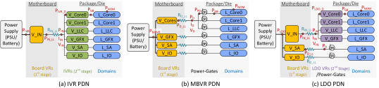
Fig. 1 shows the high-level organization of each of the three commonly-used PDNs in modern client processors: 1) integrated voltage regulator (IVR [21, 88, 117, 61]; Fig. 1(a)), 2) motherboard voltage regulator (MBVR [97, 63, 29, 41]; Fig. 1(b)), and 3) low dropout voltage regulator (LDO VR [111, 112, 18, 15, 120, 113]; Fig. 1(c)).
Integrated Voltage Regulator (IVR) PDN. The IVR PDN is a state-of-the-art PDN in modern client processors and is used in Intel’s 4th, 5th, and 10th generation Core processors [21, 88, 61]. The IVR PDN integrates most of the SVR components (i.e., diodes, capacitors, control modules, and switches) into the processor die while some components are placed on the package ( e.g., interconnections) and off-chip (e.g., inductors). Since circuit elements in modern processors cannot tolerate the high input voltage of a power supply (–) due to their small process technology node size, the IVR PDN regulates voltage in two-stages, as illustrated in Fig. 1(a). The first stage of voltage conversion is handled by a single motherboard SVR (i.e., VR), which converts input voltage from the power supply unit (PSU) or battery (–) to a level typically less than (e.g., ). The second stage is handled by an integrated SVR (i.e., IVR), which is a sequential buck converter that converts the input voltage (i.e., output of the first stage VR) to the desired voltage level (typically –) of a processor domain (e.g., a CPU core). In a processor, multiple IVRs are used (e.g., six as shown in Fig. 1(a)) to supply different voltage levels to each processor domain.
The IVR PDN has two main advantages over other PDNs: 1) it enables fast voltage level changes, 2) it reduces a chip’s input (i.e., output of the first stage VR into the processor die) current by using a high input voltage level (e.g., compared to – using a traditional MBVR), thereby reducing power losses, and reduces the maximum current (i.e., ) requirement of the first stage VR. However, the IVR PDN has three main disadvantages over other PDNs: 1) low power-conversion efficiency in computationally light workloads due to the two-stage voltage regulation [41], 2) high design complexity as it is normally designed along with the chip , which adds extra design constraints and consumes silicon die area [86], and 3) higher sensitivity to di/dt noise than the MBVR PDN due to a limited amount of decoupling capacitors available on the processor’s die [86].
Motherboard Voltage Regulator (MBVR) PDN. The MBVR PDN is the traditional PDN for processors and is used in Intel’s 2nd, 3rd, 6th, 7th, 8th and 9th generation Core processors [97, 63, 29, 130, 131]. As shown in Fig. 1(b), the MBVR PDN uses several one-stage motherboard SVRs and multiple on-chip power-gates. An MBVR PDN has four advantages over other PDNs: 1) it decouples the VR design from the processor design, thereby reducing system design complexity, 2) heat generated due to VR power conversion losses is kept outside the processor chip, 3) it enables placing enough decoupling capacitors on motherboard, package and die (due to the long path from processor die to the off-chip VR) to reduce voltage noise, and 4) it is efficient at executing computationally light workloads. However, the MBVR PDN has two major disadvantages: 1) voltage level changes are slow as the VR is far from the load (i.e., processor domain), and 2) computationally-intensive (high current) workloads suffer high power losses due to high processor input current and high impedance (load-line) on the path from the board VRs to the processor domains.
Low Dropout Voltage Regulator (LDO) PDN. The LDO PDN is used in AMD’s recent Zen [111, 112, 15] processors. As shown in Fig. 1(c), the LDO PDN statically allocates two types of VRs to different domains based on their power demands: it allocates 1) one-stage motherboard SVRs (similar to MBVR PDN) to domains with a low and narrow power range (e.g., IO and SA) and 2) two-stage VRs for domains with wide power range (e.g., CPU cores, graphics engines, and LLC). The first stage is a single motherboard SVR (i.e., VR) and the second stage is an integrated LDO VR. Multiple LDO VRs are used (e.g., four as shown in Fig. 1(c)) which supply different voltage levels to each of the processor domains. For the two-stage VR, the processor’s power management unit adjusts to the maximum voltage required across all domains. For domains that require the same voltage level as the input voltage, the domain’s LDO VR operates in bypass-mode to avoid voltage regulation by simply connecting the input voltage signal to the output. For other domains that require a lower voltage, the LDO VR adjusts the input voltage by operating in regulation-mode. For idle domains, the LDO VR acts as a power-gate.
The LDO PDN has three advantages over other PDNs: it 1) requires less board area compared to the MBVR PDN, 2) is simpler than the IVR PDN as the integration of an LDO VR into the die is simpler than that of an SVR, 3) has higher power-conversion efficiency than an IVR PDN when running computationally light workloads. However, the LDO PDN has two main disadvantage s compared to other PDNs: 1) low power-conversion efficiency in computationally intensive workloads due to the high processor input current and high impedance (load-line) on the path from the board VRs to the processor domains, and 2) higher design complexity than MBVR as it is designed along with the chip , which adds extra design constraints and complexity to the power management algorithms.
2.4 VR and PDN Parameters
Power-Conversion Efficiency (). The ratio of the total output power () of a VR to the total input power () is known as Efficiency () as given in Equation 1.
|
|
(1) |
For an SVR, power-conversion efficiency is not constant, but rather a function of: 1) the load current and 2) the input and output voltages [40, 39, 34, 12]. The LDO VR power-conversion efficiency, , is the ratio of the desired output voltage, , to the input voltage, , times the LDO VR current efficiency (typically around 99% in a modern LDO VR [79, 50]), thus .
The power-conversion efficiency is also defined for the entire PDN, also known as the PDN end-to-end power-conversion efficiency (ETEE). ETEE of a PDN at a given time is the ratio between the total load’s nominal power (i.e., the sum of all loads’ nominal power444 A load’s nominal power at a given time is a function of the load’s 1) power state (e.g., active vs. idle), 2) activity factor, 3) frequency, 4) nominal voltage, and 5) temperature [45, 39, 40, 34].) and the effective power consumed by the main power supply (e.g., battery, PSU).
VR Tolerance Band (TOB). The tolerance band (TOB) of a VR [58] is the maximum voltage variation for the VR across temperature, manufacturing variation, and age factors (e.g., ). The standard VR TOB can be sliced into three main categories: controller tolerance, current sense variation, and voltage ripple. The supply voltage is maintained at a higher value than the nominal voltage required by the load , to compensate for TOB voltage variations. This excess voltage due to the TOB leads to wasted power that cannot be utilized by the load.
Application Ratio (AR). AR is a term used in power/performance modeling to quantify the computational intensity of a workload [34]. AR describes the switching rate of a processor component (e.g., CPU core, graphics engine, IO) for a workload when compared to the highest possible power, , that can be consumed by the most computational ly-intensive workload (i.e., also known as the power-virus workload [88, 77, 31]). AR and can be estimated 1) offline using power modeling tools such as McPAT[77], SYMPO [31] or Intel’s Blizzard [9]), and 2) at runtime using activity sensors implemented in the processor components [7, 126, 10, 110, 102, 78, 19, 30].
Load-line. The load-line or adaptive voltage positioning [59] is a model that describes the voltage and current relationship under a given system impedance (). This relationship is defined as: where and are the voltage and current at the load, respectively. is the tolerance band (TOB) voltage variation and is the input voltage to the system. From this equation, we can see that the voltage at the load input () decreases when the current of the load () increases (e.g., when running a workload with a high AR). Therefore, to keep the voltage at the load () above a minimum functional voltage under even the most computationally-intensive workload (i.e., power-virus [88, 77, 31], for which AR=1), the input voltage () is set to a level that provides enough guardband.
3 PDNspot
We develop PDNspot, a framework that models the three commonly-used PDNs in modern client processors, evaluating multiple metrics of interest (i.e., performance, energy, BOM, and board area). PDNspot provides a versatile framework that enables multi-dimensional architecture-space exploration of modern processor PDNs. PDNspot evaluates the effect of multiple PDN parameters, TDP, and workloads on the metrics of interest. In this section, we present the core models of PDNspot: 1) an end-to-end power-conversion efficiency (ETEE) model for each PDN that we use to assess the average power and current consumption of a PDN, 2) board area and BOM models, and 3) a performance model of the processor that we use to assess each PDN’s impact on performance.
3.1 End-to-End Power-Conversion Efficiency
(ETEE) Modeling
We present three high-level power models. Each model takes multiple inputs (main inputs tabulated in Table 2) to calculate the end-to-end power consumption of a domain (shown on the right side of each PDN in Fig. 1), starting from nominal power of each load (, in Fig. 1) until the power supply (shown on the left side of each PDN in Fig. 1). The calculations follow the symbols shown in Fig. 1 on each PDN to estimate the total power (i.e., , , and ) consumed by the main power supply (i.e., PSU or battery).
We calculate the end-to-end power-conversion efficiency (ETEE) of each PDN as the ratio of the total input power of the PDN (i.e., the sum of the nominal input power of all loads, ) to the total effective power (i.e., , , and ) consumed by the main power supply. We begin by discussing MBVR PDN modeling as it is the simplest PDN.
| Parameter | IVR | MBVR | LDO |
| Load-line Impedance (m) | |||
| VR Tolerance Band (mV) | – | – | – |
| On-chip VR Efficiency | – | — | |
| Off-chip VR Efficiency | power-state– | ||
| Leakage Fraction | – depending on the domain | ||
| Cores Nom. Power (W) | – for TDP range – | ||
| LLC Nom. Power (W) | for TDP range – | ||
| GFX Nom. Power (W) | – for TDP range – | ||
| PG Impedance (m) | – depending on the domain | ||
MBVR PDN Power Modeling. In order to calculate the total power consumption of the MBVR, denoted by (), we first calculate , which is the power consumption after applying a voltage guardband on the nominal power . This voltage guardband, , guarantees proper circuit timing across voltage variations ( explained in Sec. 2.4). The leakage and dynamic power consumption scale differently as voltage increases from to (i.e., when nominal voltage, , is increased by a voltage guardband, ). The dynamic power consumption is proportional to the voltage squared (i.e., ), while the leakage power consumption scales exponentially with voltage and depends on several other parameters such as threshold voltage, temperature, and other design and fabrication characteristics [40, 39, 64, 34, 45]. As an approximation, we use a model based on polynomial curve fitting, where leakage power scales polynomially with supply voltage (i.e., ). We validate our model with measurements on a commercial client processor (Intel Core i7-6600U Processor [55]). Assuming the same temperature, the leakage power scales by the power of 2.8 proportional to voltage scaling. We assume a leakage fraction () of for the graphics domain and for the rest (e.g., cores, LLC, SA) similarly to Rusu et al. [103]. Therefore, can be calculated with Equation 2.
|
|
(2) |
For domains with power-gates (e.g., and in Fig. 1(b)), there is an additional voltage drop on the power-gate (, e.g., ) due to its impedance (). The power consumption ( in Fig. 1(b)), due to this increase in the supply voltage, is calculated similarly to Equation 2 (i.e., by assigning in the equation: , , () instead of , , , respectively).
Next, we need to compensate for the voltage drop on the load-line impedance (, discussed in Sec. 2.4) by raising the on-board VR output voltage (i.e., applying a voltage guardband). The voltage guardband needs to account for the maximum possible voltage drop, which is attained when the processor consumes the maximum possible power, , by running the most computationally-intensive workload, which is also known as a power-virus workload [88, 77, 31]. Next we attain, , the total power consumption of a group of domains which share the same off-chip VR (e.g., , ), by summing all values from each domain,. We use the application ratio (AR, discussed in Sec. 2.4), to obtain by scaling using the AR, i.e., . The corresponding calculation for the voltage and power after accounting for the voltage drop on the load-line impedance of each group of domains (i.e., in Fig. 1(b)) is shown by Equations 3 and 4, respectively.
|
|
(3) |
|
|
(4) |
The total power, , consumed from the battery/PSU is obtained by summing the effective power of each domain, which can be calculated by dividing the output power of each on-board VR by its power conversion efficiency () as shown in Equation 5.
|
|
(5) |
IVR PDN Power Modeling. Using the same approach for modeling MBVR PDN power consumption, we calculate the total power of an IVR PDN, , consumed from the battery/PSU, as shown in Fig. 1(a). We calculate by applying a voltage guardband due to the VR tolerance band (i.e., TOB, discussed in Sec. 2.4) using Equation 2. (in Fig. 1(a)) is the power consumption after accounting for the IVR loss at a specific domain. Given the IVR power conversion efficiency , can be calculated using Equation 6.
|
|
(6) |
Next we calculate (shown in Fig. 1(a)) by summing the power consumed by all domains connected to VR (i.e., ). Similarly to the MBVR PDN, the voltage () and power consumption () after accounting for the voltage drop on the load-line impedance (i.e., ) are calculated with Equations 7 and 8, respectively, whereas . Finally, we obtain the total power () consumed from the battery/PSU by dividing the output power (i.e., ) of the VR by the power conversion efficiency of the VR ( i.e., ), as shown in Equation 9.
|
|
(7) |
|
|
(8) |
|
|
(9) |
LDO PDN Power Modeling. Similarly to the other two models, (shown in Fig. 1(c)) is calculated using Equation 2. For the four domains with LDO VRs (i.e., , and domains), we calculate the power of each domain after including the LDO VR power conversion losses, denoted by in Fig. 1(c). is obtained by dividing the output power of the LDO () by the power conversion efficiency of the LDO () as shown in Equation 11. is the ratio of the desired output voltage to the input voltage multiplied by the LDO VR current efficiency (, e.g., 99%), as shown in Equation 10. Next, we obtain the power that each LDO domain consumes from the shared VR () using two steps. First, we sum the power of each LDO domain to obtain (i.e., ). Second, we calculate the power consumption () after accounting for the voltage drop on the load-line impedance (i.e., ) using Equations 7 and 8 (similar to the calculations in IVR PDN power modeling).
|
|
(10) |
|
|
(11) |
For domains that use motherboard VRs (i.e., and ), we calculate the power () that each of these domains consumes from the motherboard VRs (i.e., and ) using Equations 3 and 4 (similar to our calculations in MBVR PDN power modeling). Finally, the total power (i.e., ) that the LDO PDN consumes from the battery/PSU is calculated by summing the power that each motherboard VR consumes from the battery/PSU as shown in Equation 12.
|
|
(12) |
3.2 Board Area and BOM Modeling
The board area and BOM of an off-chip VR are functions of mainly the maximum current () that the VR can support. is the maximum current that the VR must be electrically designed to support. Exceeding the the limit can result in irreversible damage to the VR or the processor’s chip [34, 40, 39, 62, 59, 86, 135, 141, 80]. A higher implies a larger VR and higher cost. VR sharing between multiple domains (e.g., the LDO PDN shares VR for cores, LLC, and graphics as shown in Fig. 1(c)) effectively reduces the maximum current required, , thereby reducing the area and BOM of the off-chip VR.
To reduce system area and cost, many platforms use a power management integrated circuit (PMIC [134, 52, 109]) that incorporates multiple VRs (and other functions) into one integrated circuit. In our model, the VR area and cost are calculated based on the requirements for each domain of a PDN. We assume an optimized solution with a PMIC for processors with TDPs up to for all PDNs. Higher -TDP processors typically use a traditional voltage regulator module (VRM [59]) instead of a PMIC due to the high current requirements of these processors [52, 109]. We obtain the actual mapping between the and the area/cost directly from Texas Instruments VR vendor [118].
3.3 Processor Performance Modeling
To understand the impact of PDN end-to-end power-conversion efficiency (ETEE) on workload performance of a client processor, we build a performance model. Our performance model aims to estimate the performance improvement of a CPU- (graphics-) intensive workload when increasing the power-budget allocated to the CPU cores (graphics engines).
We build the performance model of the compute domain (i.e., CPU cores and graphics engines) using empirical measurements on a real system in three steps. First, we run a CPU- (graphics-) intensive workload with high performance-scalability555 We define performance scalability of a workload with respect to CPU frequency as the performance improvement the workload experiences with unit increase in frequency, as described in [139, 46]. Modern processors predict the performance-scalability of a workload at runtime using performance counters [139]. The performance-scalability metric is used by current power management algorithms, such as Intel’s SpeedShift [98] and EARtH [27], which first appeared in the Intel Skylake processor [8]., e.g., 416.gamess of SPEC CPU2006 [114] (3DMark06[124]), on a real Intel Skylake system , whose specifications are in Table 3. Second, we sweep the frequency of CPU cores (graphics engines) in steps of 100MHz (50MHz), the finest CPU core (graphics engine) frequency granularity that the Skylake architecture supports. Third, we measure the total power consumption of the processor and log the increase in power consumption compared to the measurement done in the previous (i.e, lower) frequency. By doing so, we build power-frequency curves that we use along with the workload’s performance-scalability to estimate performance as a function of power.
Using our performance model, we plot in Fig. 2(a) the additional power-budget required (y-axis) to increase the clock frequency of a CPU/graphics domain by when running CPU-/graphics-intensive workloads, relative to the baseline frequency of each TDP (x-axis). We observe that, compared to a high-TDP (e.g., ) processor, a low-TDP (e.g., ) processor requires only a small amount of power (e.g., ) to increase the clock frequency of a CPU/graphics domain by . Fig. 2(b) shows the percentage (y-axis) of the total TDP power-budget (x-axis) that is allocated to the CPU-cores, LLC, IO and SA, and PDN power losses for a CPU-intensive workload (no budget is allocated to graphics in this workload). In each TDP, we use the PDN among three commonly-used PDNs (i.e., MBVR, IVR, LDO) that maximizes PDN power loss (e.g., IVR for and MBVR for ), to show the effect of using an unoptimized PDN on different processor domains’ power budgets. We find that in a low-TDP processor, a relatively small fraction (e.g., only of a TDP) is allocated to CPU-cores compared to a higher-TDP processor (e.g., about of a TDP), while PDN power loss is or more (i.e., ETEE of or less). If we use a PDN with a higher ETEE for each TDP (e.g., higher ETEE , which translates to lower PDN power loss), we can increase the CPU-cores’ power-budget by the spared power on PDN loss (e.g., ), thereby increasing the workload’s performance. We illustrate the impact of a PDN’s ETEE with the following example.
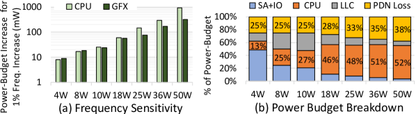
Impact of PDN ETEE on System Performance. For a TDP processor, the domains’ nominal power consumption (i.e., the sum of each domain’s nominal power consumption) is approximately 3W. To find the total processor power consumption, we must account for the PDN power conversion loss by dividing the domains’ nominal power consumption by the PDN’s ETEE. Therefore, the PDN’s ETEE can dictate the amount of remaining power budget for reallocation across the domains to improve system performance. For example, we can increase the CPU-cores’ clock frequency by 1% for each 9mW increase in the CPU-cores’ power budget at a TDP (shown in Fig. 2(a)).
To show how even a small difference in ETEE can have a significant impact on system performance, assume we have two PDNs: 1) with =, and 2) with =. The total processor power consumption of and are () and (), respectively. According to our model (shown in Fig. 2(a)), the additional () saved by using (instead of ) could be allocated to increasing the CPU cores’ clock frequency by . This would increase the performance of a highly-scalable workload by .
3.4 PDNspot Assumptions and Limitations
Assumptions. Our PDNspot model makes three main assumptions. First, PDNspot assumes that the system operates within a thermal design power (TDP) limit. The power management unit allocates 1) a power-budget to the SA and IO domains, which have nearly constant power consumption across different TDPs, and 2) the remaining power-budget to the compute domain (cores and graphics). The compute domain power-budget is divided between the cores and the graphics engines based on the running workload (e.g., CPU- versus graphics-intensive workload). Second, PDNspot assumes the same routing resources for all PDNs. Therefore, for PDNs in which multiple domains share a single VR (e.g., IVR, LDO), the routing resources of these domains are combined. Third, PDNspot assumes that all voltage emergencies are handled by both 1) existing decoupling capacitors and 2) existing architectural techniques. This is a reasonable assumption for modern client processors [102, 7, 112].
Limitations. Our PDNspot model has two main limitations. First, the model predicts the ETEE based on average values of inputs over a time interval (e.g., during residency in a power state). To provide the dynamic ETEE of a workload (e.g., during multiple system power states within a workload), PDNspot should be run for each time interval separately with the appropriate input for the examined time interval. However, this is not a big limitation since doing so can be automated (e.g., using a script) once data for multiple intervals is collected. Second, the model considers the processor and the off-chip VRs as a single thermal domain (i.e., as sharing the same TDP), which is true for many systems [92]. However, the PDNspot model does not provide the effect of thermals on power and performance for a system in which the processor and off-chip VRs are in two different thermal domains.
4 PDNspot Validation
PDNs in modern client processors have complex designs, and they involve several components integrated on die, package, and board. For example, the IVR design includes multiple components such as 1) buck regulator bridges [21], 2) control modules that generate the pulse width modulation (PWM) signals [49, 93, 73] and activate IVR phases, 3) air core inductors (ACI) [21, 49], and 4) Metal Insulator Metal (MIM) capacitors [21]. In addition, several IVR parameters (e.g., thresholds for voltage-regulator power-states) and algorithms (e.g., phase-shedding management) are typically configured and tuned post-silicon. Therefore, modeling these designs with, for example, SPICE [87] is inaccurate and unsuitable for validating our power models. Instead, we obtain the input parameters (shown in Table 2) to PDNspot and validate the three power models of PDNspot with real experimental data from our lab that we collect using two different sets of benchmark traces that are typically used to evaluate client processors.
In this section, we present the 1) experimental setup used to obtain PDNspot model parameters, 2) methodology for obtaining PDNspot model parameters, and 3) PDNspot validation process.
4.1 Experimental Setup
System Setup. To measure power and validate our power models, we use two systems with the configurations shown in Table 3. Intel Broadwell and Skylake architectures use IVR [88] and MBVR [26] PDNs, respectively.
Benchmark Traces. To obtain the input parameters (shown in Table 2) for our models and validate the models, we use approximately 5000 traces from a wide variety of benchmarks, typically used in evaluating client processors. We use single threaded traces, multi-programmed traces, and graphics traces comprising of 1) representative CPU- and graphics-intensive workloads including SPEC CPU2006 [114], Sunspider [128], PhotoShop [2], Illustrator[1] SYSmark [14], HandBrake [133], 3DMark06[124], Crysis [28], 2) representative battery life workloads such as office productivity workloads (e.g., MobileMark[13]), video conferencing and streaming workloads, and web-browsing workloads [6], and 3) synthetic traces of power-virus [26] for each domain , which can be generated using tools such as McPAT[77], SYMPO [31] or Intel’s Blizzard [9].
Power Measurements. For the platform power measurements, we use a Keysight N6705B DC power analyzer [69] equipped with an N6781A source measurement unit (SMU) [70]. The N6705B (equipped with N6781A) accuracy is around [70]. The power analyzer measures and logs the instantaneous power consumption of different device components. Keysight’s control and analysis software [69] is used for data visualization and measurement management. For more detail, we refer the reader to the Keysight manual [69] and to our prior work [42].
4.2 Obtaining PDNspot Model Parameters
We describe the process we use to obtain each of the input parameters to PDNspot models. A summary of the main parameters is shown in Table 2.
VR Efficiency Curves – Input Parameters. We measure two sets of parameters for 1) on-chip VR efficiency (i.e., and ) and 2) off-chip VR efficiency (i.e., , , , and ). We perform the measurements on our systems across multiple values in the operational range of the 1) VR input voltage (e.g., 7.2V, 9V, 12V for off-chip VR; 1.6V and 1.8V for IVR), 2) VR output voltages (e.g., 0.5V, 0.6V, 0.7V, 1V, 1.8V), and 3) load current.
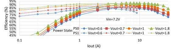
We measure the off-chip VR efficiency (, , , and ) by 1) connecting the VR input (output) to channel A (B) of the DC power analyzer, which we configure as the power supply ( DC electronic load) [71]. This setup enables us to 1) measure the input and output power, and 2) sweep over the ranges of the load current, output voltage and input voltage values, and log the data into the host PC that runs the control and analysis software. We also measure the efficiency for each VR power-state for VRs that support multiple power-states (e.g., supports PS0, PS1, PS3 and PS4). Fig. 3 shows the efficiency curves for the off-chip VRs (i.e., , , , and ) as a function of multiple output voltages, one input voltage (7.2V) and two VR power-states (PS0 and PS1).
We measure IVR efficiency () using the Broadwell processor. Since the IVR is integrated into the processor, it is impossible to disconnect the native load (e.g., cores, graphics engines) and connect a high current load directly to the output of an IVR. Therefore, to measure the IVR efficiency, we operate the processor in a special Design For Test (DFT) mode [21]. We also operate the processor clock tree at varying frequencies to enable a large effective adjustable load current. We measure the current and voltage at the output and input (i.e., output of the in Fig. 1) of the IVR [21]. Next, we calculate the input and output power and plot the efficiency curves as a function of load current and output voltage. Table 2 (On-chip VR Efficiency) shows the range of the measured IVR efficiency (–). The actual curves in PDNspot plot the efficiency as a function of input voltage, output voltage and output current.
We measure the LDO VR efficiency () in two steps. First, since the LDO VR is not implemented in our experimental systems, we emulate the LDO VR static behavior using the power-gates that exist in the MBVR PDN of the Skylake processor, a technique666By controlling the number of the conducting power-gate transistors and their gate voltages, the power-gate behaves like an LDO VR. The actual LDO VR implementation has additional circuitry (e.g., to handle load transient response, digital control of the LDO VR output). which is used by Intel [79] to implement an LDO VR. Second, we measure the input and output power of the LDO VR under varying load current, input and output voltages and plot the efficiency curves. The LDO VR efficiency is the ratio between the output and the input voltage times the ratio between input and output current (also known as current efficiency), i.e., . Our measurements show that the current efficiency, i.e., , is more than as tabulated in Table 2.
Nominal Power of Domains – Input Parameter. We measure the nominal power () input parameter of each domain (i.e., cores, LLC, graphics, SA, and IO) directly on the Skylake system when running traces of single threaded, multi-threaded and graphics workloads. We log the measured power of each trace and its application ratio (i.e., , discussed in Sec. 2.4).
Other Input Parameters. We measure the Load-line impedance () from a domain’s input to the output of the off-chip VRs for each domain directly on Skylake and Broadwell Systems. We measure peak-power (i.e., ) when running power-virus traces. We estimate leakage-power fraction () using a post-silicon technique, thermal conditioning [25, 47, 23], by 1) increasing the processor temperature while running a load with constant voltage and frequency (i.e., constant dynamic power), 2) measuring the associated changes in power consumption, and 3) extrapolating the domain’s power fraction which is affected by temperature, as the leakage power depends exponentially on temperature whereas the dynamic power is not affected by temperature [40, 39, 64, 34].
4.3 PDNspot Validation
We validate PDNspot by comparing the predicted ETEE obtained from each PDNspot model (i.e., IVR, MBVR, and LDO) with the ETEE measurements on real systems.
To validate PDNspot, we use as reference the total power consumption of real Intel processors (Broadwell, Skylake, and Skylake with emulated LDO PDN) measured from the main power supply (battery/PSU) for each of the PDNs (, , and ). We use PDNspot to obtain the predicted power consumption of each PDN. We use a subset () of the benchmark traces (single-thread, multi-programmed, and graphics described in Sec. 4.1) that have various application ratios (AR). We calculate the measured (predicted) ETEE of each PDN by dividing the total nominal power consumption (i.e., PDN output power) by the measured (predicted) total power consumption (i.e., PDN input power). Finally, we calculate the accuracy of PDNspot by comparing the measured ETEE to the predicted ETEE of each PDN.
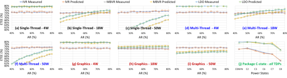
We find that our three IVR, MBVR and LDO PDN models in PDNspot have an average (min/max) accuracy of (/), (/), and (/), respectively, across all our workloads. Fig. 4(a–i) shows the validation results (measured vs. predicted ETEEs) for , , TDPs when running single-threaded, multi-programmed, and graphics traces with an AR between to . Fig. 4(j) shows the results for the battery life related power-state s: C0 with minimum frequency () and package C-states (C2/3/6/7/8) [40, 39, 34].
5 Motivation: PDN Inefficiencies in Client Processors
This section makes three key empirical observations about the three most commonly-used PDN architectures (i.e., IVR [21, 88, 61], MBVR [97, 63, 29], LDO [111, 112, 18, 15, 120, 113]) in modern high-end client processors to motivate the need for a hybrid and adaptive PDN that leverages the advantages of each one of the three PDN architectures.
We use our validated model, PDNspot, to evaluate the efficiency of the three PDNs. We estimate the off-chip current consumption, ETEE with breakdown into multiple sources of power-conversion losses, and average power consumption of a processor using each of the three PDNs. We use a total of 300 CPU-intensive, graphics-intensive, and video playback workload traces to evaluate each PDN.
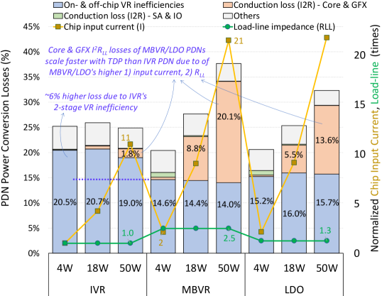
Observation 1. We observe that when executing CPU- and graphics-intensive workloads, the IVR PDN has a lower ETEE at the TDP (Figures 4.a,d,g) and a higher ETEE at the TDP (Figures 4.c,f,i) compared to MBVR and LDO PDNs across the entire range of tested ARs. The ETEE crossover point , at which the IVR ETEE becomes higher than the MBVR/LDO ETEE, exists at some TDP between and .
Fig. 5 provides more insight into this observation with breakdowns of PDN power conversion loss. We find that at TDP, the dominating contributor to the PDN power conversion loss are the on-chip and off-chip VR inefficiencies. At TDP, the IVR PDN has a lower ETEE than the MBVR and LDO PDNs due to the higher power conversion inefficiencies of the IVR PDN’s on-chip and off-chip VRs. At a TDP, we find that MBVR and LDO PDNs have lower ETEEs due to their high loss in core and graphics domains. The high loss is due to: 1) a higher chip input current in the MBVR and LDO PDNs compared to the IVR PDN777The IVR PDN reduces the chip input current because it uses high input voltage from the first-stage VR into the chip (Sec. 2)., and 2) a higher load-line impedance () in the MBVR/LDO PDNs compared to the IVR PDN888The IVR and LDO PDNs have lower compared to MBVR because both IVR and LDO PDNs share routing resources from external VRs into the chip’s package and die.. We conclude that the MBVR and LDO PDNs are more efficient at a low TDP (e.g., ) compared to the IVR PDN, while the IVR PDN is more efficient at a high TDP (e.g., ).
Observation 2. We observe that the PDN ETEE is affected not only by the TDP (as discussed in Observation 1) but also by the workload’s Application Ratio (AR) and the workload type, i.e., single-threaded, multi-threaded, and graphics.
Fig. 4(a–i) shows that the MBVR and LDO PDN ETEEs increases with AR, which is most pronounced at 18W and TDPs. This phenomenon is due to the load-line (described on Sec. 2), which results in a lower voltage-guardband when running workloads with higher ARs.
Fig. 4(b,e,h) show that the single-thread, multi-thread, and graphics workloads (all at the same TDP of 18W) have different ETEE curves. For example, for the graphics workload in Fig. 4(h), the IVR PDN is less efficient than the other two PDNs for the entire AR range (with a crossover point around 21W TDP, not shown in Fig. 4 , at which the IVR ETEE becomes higher than the MBVR/LDO ETEE), while the other two workloads have crossover points at different ARs within the 18W TDP.
Fig. 4 (a–f) shows that the LDO ETEE is higher than the MBVR ETEE for CPU-intensive (single- and multi-threaded) workloads, but is lower than the MBVR ETEE for graphics-intensive workloads. Note that the LDO inefficiency is more dominant in graphics workloads, due to the high voltage difference between the core and graphics domains because in graphics-intensive workloads, the graphics-engine runs at relatively high frequencies (and voltages) while cores are kept at low frequencies (and voltages). Therefore, the LDO PDN 1) sets the off-chip (i.e., first stage) VR voltage to the high voltage level required by the graphics-engines (e.g., ) while activating the graphics-engines’ on-chip LDO (i.e., second-stage) VR in bypass-mode, and 2) uses the core’s on-chip LDO (i.e., second-stage) VR to regulate the voltage down to the low voltage level required by the core (e.g., ). Doing so, results in very low power conversion efficiency of the core’s LDO VR (e.g., , as discussed in Sec. 2.2), thereby reducing the ETEE of the LDO PDN.
We conclude that, in addition to the TDP, the AR and workload type have significant effects on each PDN’s ETEE. Particularly, lowering the workload’s AR degrades the ETEE of MBVR and LDO PDNs due to load-line effect, while using graphics -intensive workloads reduce the LDO ETEE compared to CPU-intensive workloads due to the high voltage requirement difference between the core and graphics domains.
Observation 3. We observe that the ETEE of the IVR PDN is significantly lower than that of MBVR and LDO PDNs for computationally light workloads (e.g., video playback, web browsing, office productivity applications [13, 6, 14]) and low-power states across all TDPs. Fig. 4(j) shows the ETEE of the three PDNs in 1) , an active power-state in which the core and graphics domains operate at their lowest frequencies, and 2) package C-states (C2, C3, C6, C7, and C8 [40, 39, 34]), low power-states of the processor. The processor uses these power-states, for all TDPs, to reduce energy consumption (thereby increasing battery life of battery-powered devices) when the processor runs a light (i.e., low computational intensity) workload or once the processor is partially/fully idle. We explain the effects of ETEE in these power-states on battery life using a video playback workload example.
The video playback [6] workload is a computationally light workload that operates in three main power-states during each video-frame. First, a power-state, which consumes = nominal power for = ( is the residency of power state in terms of the fraction of execution time) of the frame’s time. In this state, the cores and graphics engines prepare a video-frame and store it in main memory. Second, a power-state, which consumes = nominal power for = of the frame’s time. The cores and graphics engines are idle (power-gated) in this state. In , the display-controller fetches part of the frame from main memory into a local buffer inside the display controller. Third, a power-state, which consumes = nominal power for = of the frame’s time. In , the display controller reads frame data from its local buffer and displays it on the display panel, while the rest of the processor is idle (e.g., main memory is in self-refresh). We calculate the average power of the video playback workload by summing the fractional power of each power-state taking into account the ETEE in each state (denoted by ). Hence, the average power is given by: . The video playback average-power results (shown in Fig. 8(c)) show that MBVR and LDO PDNs have and lower average power , respectively, than the IVR PDN. We conclude that the IVR PDN is energy-inefficient for computationally-light workloads, which negatively impacts both energy consumption and battery life.
Summary. We conclude that there is no single PDN for modern client processors that maintains a high ETEE across all TDPs, workload types and application ratios (ARs). These observations motivate us to build a hybrid and adaptive PDN that utilizes the advantages of each one of the three PDN architectures, as we describe in Sec. 6.
6 FlexWatts
We present FlexWatts, a hybrid adaptive PDN for modern processors that maintains a high ETEE for the wide power consumption range and workload diversity of client processors. FlexWatts is based on three key ideas. First, it combines IVRs and LDOs in a novel way to share multiple on-chip and off-chip resources and thus reduce BOM, as well as board and die area overheads, as illustrated in Fig. 6. This hybrid PDN is allocated for processor domains with a wide power consumption range (e.g., CPU cores and graphics engines) and it dynamically switches between two modes, IVR-Mode and LDO-Mode, based on the efficiency of each mode, using a special power-management flow. Second, FlexWatts statically allocates an off-chip VR to each system domain with a low and narrow power consumption range (i.e., SA and IO domains). This is because unlike in compute domains, the power consumption of the system-agent (SA) and IO domains does not significantly scale with TDP (as shown earlier in Fig. 2(b)) or workload’s AR. Thus, it is more energy-efficient to place each of them on a dedicated off-chip VR compared to using an on-chip VR999AMD uses the same strategy for their LDO PDNs [112] (Fig. 1(c)). Third, FlexWatts introduces a new prediction algorithm that automatically determines which PDN mode (IVR-Mode or LDO-Mode) would be the most beneficial based on system and workload characteristics. For example, FlexWatts can operate in LDO-Mode (IVR-Mode) when the processor runs a light (heavy) workload such as video playback (Turbo Boost), or when the processor operates at low (high) TDP such as (). FlexWatts uses a runtime ETEE prediction algorithm to select the operation mode (i.e., LDO-Mode or IVR-Mode) that maximizes ETEE.
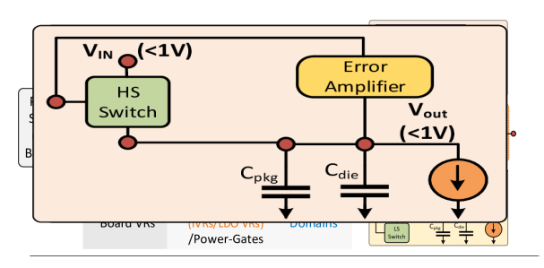
Hybrid PDN and Resource Sharing. We build the FlexWatts PDN by modifying a baseline IVR PDN, shown in Fig. 1(a), in two ways. First, we replace the two on-chip IVRs of the SA and IO domains (i.e., V_SA and V_IO IVRs) with two off-chip VRs and two on-chip power-gates, as illustrated in Fig. 6. Second, we implement hybrid VRs , which extend each of the remaining IVRs (i.e., V_Core0/1, V_LLC and V_GFX IVRs in Fig. 1(a)) by implementing an LDO VR using the existing resources of the IVR, as illustrated in Fig. 6 (right side). By doing so, we enable a hybrid PDN that has two modes of operation, IVR-Mode and LDO-Mode, with low cost and low area overhead. As illustrated in Fig. 6, each hybrid VR shares between the two modes 1) on chip resources such as the high-side (HS) NMOS power switch [21], and decoupling capacitors (both on package and on die) of the baseline on-chip IVR, and 2) off-chip VRs (i.e., ). We use the HS power-switch to implement the LDO VR, similar to Luria et al. [79], a work carried out by Intel that utilizes the power-gate’s power-switch to implement an LDO VR. This architecture enables both PDN modes to share routing resources and the power grid across board, package, and die during operation, as illustrated in Fig. 6.
Voltage Noise-Free Mode-Switching. FlexWatts mode-switching transitions the hybrid PDN between two modes (IVR-Mode and LDO-Mode). Carrying out the mode-switching while the compute domains are active may introduce voltage noise because the two modes have very different operation principles. In IVR-Mode, the off-chip VR () is set to a relatively high-voltage (e.g., ) and the on-chip IVRs regulate the voltage to the level the domain needs (e.g., –). In LDO-Mode, voltage is set to the maximum voltage required by all domains (e.g., –) and the on-chip LDOs regulate this maximum voltage to the level the domain needs. Therefore, the mode-switching should configure the on-chip and off-chip VRs and change their voltage levels while transitioning from one mode to the other.
To prevent any voltage noise during mode-switching, FlexWatts performs mode-switching while the compute domains are idle. To do so, we 1) place the processor in an idle power-state for a short period, 2) configure the hybrid PDN and update the on-chip and off-chip VR levels, and 3) exit the idle power-state and resume the processor with the new PDN mode. To this end, we utilize a power-management flow that places the processor into the idle power-state, (which exists in most modern processors [26, 51, 48, 121, 34, 40, 39, 42, 43]), in which the cores, LLC, and graphics units are turned off after their contexts are saved into a dedicated SRAM. We leverage the C6 package C-state power management firmware flow [42] to implement FlexWatts’s mode-switching transition flow. FlexWatts takes the following three steps to switch between two PDN modes.
First, the power management unit (PMU) places the system into the package C6 idle power state during which the PMU saves the context101010The context is stored into dedicated SRAMs, using power from an always-on VR (not shown in Fig. 1) that retains the dedicated SRAMs’ contents in idle states [42, 43]. of the hybrid PDN domains (i.e., the CPU cores, LLC, and graphics) and turns off their clock and voltage. Second, the PMU performs the actual mode switching actions of the hybrid PDN by 1) adjusting the VR voltage to a level suitable for the new mode (i.e., for IVR-Mode, or – for LDO-Mode), and 2) configuring the hybrid VRs to operate in the new mode (as illustrated in Fig. 6). Third, the PMU exits the package C6 idle power-state and switches to the active state. Doing so allows the processor to resume execution while the hybrid PDN domains use the new PDN mode.
Runtime PDN Mode-Prediction Algorithm. So far, we explained how to switch between two PDN modes (i.e., mode-switching flow) without describing when to switch. FlexWatts relies on our new runtime mode-prediction algorithm whose goal is to predict which PDN mode, among the two modes, IVR-Mode and LDO-Mode, provides the best end-to-end power-conversion efficiency (ETEE).
As shown in Fig. 4, ETEE is a function of 1) the AR and the workload type (i.e., single-thread, multi-thread, and graphics), and 2) the TDP and the power-state of the system. ETEE depends on the AR due to the load-line effect (discussed in Sec. 2.4) and shown in Equation 3. The workload type affects ETEE because each of the three workload types stresses the underlying power delivery network differently, as explained in Sec. 3.1.
Algorithm 1 depicts our mode prediction algorithm. The key idea of our algorithm is two-fold. First, we store two sets of ETEE curves inside the PMU firmware, one set for the IVR PDN and the other set for the LDO PDN. A PDN ETEE curve set is a multidimensional table111111A modern PMU implements multiple curves (as tables) such as leakage power as function of temperature and voltage, voltage as function of frequency, VR power-conversion efficiency as a function of input-voltage, output-voltage and output-current[40, 39, 34, 101, 98]. that includes an ETEE curve corresponding to a TDP for each workload type (i.e., three curves for each TDP point). Each ETEE curve stores the ETEE values as a function of the AR (as shown in Fig. 4(a-i)). We also include one ETEE curve for power states (as shown in Fig. 4(j)). Second, for every evaluation interval (e.g., 10ms), we estimate each of the algorithm’s input parameters (i.e., TDP, AR, workload type, and power-state). We use the estimated parameters to access the corresponding ETEE curve to obtain the ETEE values for both IVR-mode and LDO-mode. The algorithm chooses the mode that maximizes the ETEE. Next, we explain how we estimate the inputs to our algorithm (i.e., TDP, AR, workload type, and power-state) at runtime.
Runtime Estimation of the Algorithm Inputs. The PMU of a modern processor uses the TDP, AR, workload-type, and power-state in multiple power management algorithms such as 1) power-budget management (PBM) algorithm [101, 26, 24], 2) Turbo Boost algorithm [101, 26, 98], and 3) system maximum current protection [102, 7].
The runtime-configured TDP value is available to the PMU [132, 5]. To estimate the AR, the PMU uses activity sensors [7, 126, 10, 110, 102, 78, 19, 30] that are implemented in multiple domains of the Intel Skylake processor [110, 102, 19, 26]. These activity sensors estimate each domain’s activity using internal events in each domain, such as active execution ports in the core, memory stalls, type of instructions being executed (e.g., scalar, vector instructions of 128-bits/256-bits/512-bits). A dedicated weight is associated with each event, and the weighted sum of the events in a domain is periodically (e.g., every millisecond) sent to the PMU. The weights of the activity sensors are calibrated post-silicon to provide a proxy of the AR.
The PMU estimates the workload-type (WL_TYPE) based on the power-state (i.e., active/idle) of the cores and graphics engines. For example, if the graphics engines are active, then the workload-type is set to graphics, while if more than one core is active and the graphics engines are idle, then it is set to multi-threaded.
The power-state, i.e., package power-state, of the processor is known to PMU firmware as the PMU carries out the transitions from one package C-state to another [40, 39, 34].
FlexWatts Overhead. We estimate the latency of our FlexWatts mode switching flow with techniques used by previous works that estimate the package C-state latencies [106, 105]. We find that 1) placing the processor into package C6 power state takes (without voltage changes), 2) adjusting the on-chip and off-chip VR voltage levels (assuming a latency of for on-chip VRs [21, 79], and a slew rate of [60] for off-chip VRs) takes , and 3) exiting the C6 power state takes about . Hence, the overall flow takes nearly . It should be noted that the DVFS (P-state) latency on Intel processors can take up to [37, 34, 51, 82] depending on the processor’s internal state, which shows that the FlexWatts flow latency is within an acceptable range.
The area overhead of FlexWatts over the IVR PDN is minimal. The additional area required to implement the LDO mode using the IVR resources (i.e., the high-side NMOS power switch) is around [79] at 14nm process technology node. This corresponds to only and of the Intel dual and quad core client die sizes [129], respectively.
7 Experimental Results
We evaluate FlexWatts with respect to performance, battery life, board area and bill of materials (BOM), compared to the three commonly-used state-of-the-art PDNs in modern processors: IVR, MBVR, and LDO. We also include a comparison with a hybrid PDN (used in Intel Skylake-X processors [62]) that combines IVR and MBVR PDNs, which we refer to as I+MBVR. Similar to the LDO PDN, I+MBVR uses off-chip VRs for the SA and IO domains and similar to the IVR PDN, it uses IVRs for the other domains. We evaluate the PDNs using our new PDNspot framework described in Sec. 3.
7.1 CPU and Graphics Performance
We evaluate the performance of FlexWatts compared to other PDN architectures (IVR, MBVR, LDO, I+MBVR), under the following scenarios:
We evaluate the performance of CPU- and graphics-intensive workloads assuming a fan-less system121212 The junction temperature () of a fan-less small form factor device (e.g., smartphone, tablet) is typically limited by the outer surface temperature of the device [99, 136].. Therefore, we use a junction temperature () of for TDPs between – and for TDPs higher than .
SPEC CPU2006 Benchmarks at 4W TDP. We evaluate SPEC CPU2006 [114] benchmarks with the maximum allowed frequency (i.e., 0.9GHz) for a TDP system. For these benchmarks, the two cores run at the same frequency and voltage, as in all recent client processors [21, 88, 97, 63, 29, 111]. In addition, the voltage design point for the LLC matches the core voltage domain as described in Rotem et al. [100]. Thus, the core0, core1, and LLC domains have nearly the same voltage requirements ( except for voltage variations due to manufacturing process variation).
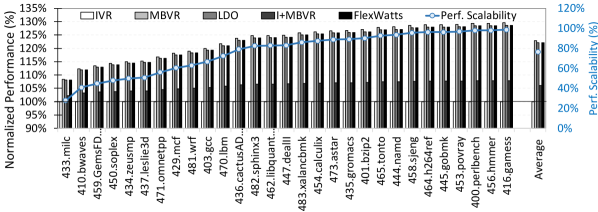
Fig. 7 plots the performance improvement (normalized to that of the IVR PDN at ) of each SPEC CPU2006 benchmark when using each of the five PDNs in a TDP system. PDNspot uses the performance-scalability metric of the SPEC CPU2006 benchmarks to estimate performance (as we discuss in Sec. 3.3). Based on Fig. 7, we make four key observations. 1) The performance improvement of MBVR, LDO, and FlexWatts, averaged across all benchmarks, is greater than for the TDP system. This is because MBVR, LDO, and FlexWatts (which mainly operates in LDO-Mode at TDP) each have a higher ETEE than IVR at low TDP. At low TDPs, IVR has a larger power conversion loss due to the two-stage ( on-chip and off-chip) voltage regulation. 2) FlexWatts has a very small (i.e., less than ) performance degradation compared to LDO and MBVR PDNs (the highest performing PDNs at TDP). FlexWatts performs only slightly worse than the LDO and MBVR PDNs due to FlexWatts’s higher load-line that is a result of resource sharing between its LDO and IVR components within FlexWatts’s hybrid PDN (discussed in Sec. 6). 3) The I+MBVR PDN provides higher performance than the IVR PDN ( on average) since I+MBVR removes the two-stage voltage regulation of the SA and IO domains. This change improves the ETEE of the I+MBVR PDN over the IVR PDN, and therefore increases the power-budget of the CPU core domain. 4) The performance improvement of the five PDNs correlates with the performance-scalability of the workloads, since the performance-scalability metric reflects how the performance of an application improves as the CPU clock frequency increases (due to the additional power-budget allocated to the CPU cores).
We conclude that FlexWatts significantly improves the CPU core performance compared to the state-of-the-art PDN (IVR) at a low TDP point by operating in LDO-Mode, which results in a higher ETEE than that of the IVR PDN.
SPEC CPU2006 Benchmarks at 4W to 50W TDP. We examine the effects of using different processor TDP levels, ranging from to , on CPU performance. Fig. 8(a) plots the average performance across the SPEC CPU2006 benchmarks for several TDP levels. Based on Fig. 8(a), we make three key observations. 1) At TDPs lower than , FlexWatts provides up to higher performance over the IVR PDN by operating mainly in LDO-Mode, which has a higher ETEE than the IVR PDN at low TDPs. Compared to the highest-performing PDNs (MBVR/LDO) at low TDPs, FlexWatts performs only slightly (i.e., less than ) worse due to the higher load-line of FlexWatts’s LDO-Mode. 2) At TDPs higher than , FlexWatts provides up to / higher performance over the MBVR/LDO PDNs by operating mainly in IVR-Mode, which has a higher ETEE than the MBVR/LDO PDNs at high TDPs. Compared to the highest-performing PDN (IVR) at high TDPs, FlexWatts performs only slightly (i.e., less than ) worse due to the higher load-line of FlexWatts’s IVR-Mode. 3) The I+MBVR PDN provides higher (up to ) performance than the IVR PDN across the tested TDP range since I+MBVR removes the two-stage voltage regulation of the SA and IO domains. This change improves the ETEE of the I+MBVR over the IVR PDN, and therefore increases the power-budget of the CPU core domain. However, I+MBVR provides significantly lower performance (up to ) than FlexWatts at low TDPs, since the I+MBVR PDN uses two-stage voltage regulation ( i.e., for the CPU cores, LLC, and graphics domains), which results in a lower ETEE compared to FlexWatts at low TDPs (e.g., ).
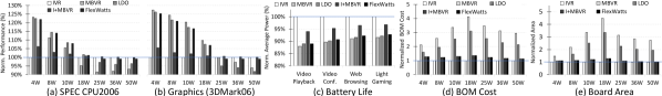
Graphics Workloads at 4W to 50W TDP. We evaluate different PDN architectures using the 3DMark06 graphics workloads [124]. While running these workloads, to of the processor’s power-budget is allocated to the CPU cores, while the rest is allocated to the graphics engines. In addition, since the graphics workloads require high memory bandwidth, the LLC domain operates at a higher frequency and higher voltage than the CPU domain.
Fig. 8(b) shows the average performance of the 3DMark06 graphics workloads with the five PDN architectures when running at to TDP. We make four key observations. 1) At TDPs lower than , FlexWatts provides up to higher performance over the IVR PDN by operating mainly in LDO-Mode, which has a higher ETEE than the IVR PDN at low TDPs. 2) At TDPs higher than , FlexWatts provides up to / higher performance over MBVR/LDO PDNs by mainly operating in IVR-Mode, which has a higher ETEE than the MBVR/LDO PDNs at high TDPs. 3) FlexWatts performs slightly worse (i.e., up to lower) than MBVR/LDO PDNs due to i) the higher load-line of FlexWatts, and ii) the large difference in operating voltages across the CPU core, LLC and graphics domains while running graphics workloads (i.e., the core domain requires low voltage, e.g., , while graphics domain requires high voltage, e.g., ), which degrades the ETEE of both FlexWatts (in LDO-Mode) and LDO PDNs (as we discuss in Sec. 2.3). 4) The I+MBVR PDN provides up to higher performance than the IVR PDN across the tested TDP range. I+MBVR improves the power conversion efficiency for the SA and IO domains (which results in I+MBVR having a higher ETEE than the IVR PDN), and increases the power-budget of the graphics domain. However, I+MBVR provides significantly lower performance (up to ) than FlexWatts at low TDPs, since the I+MBVR PDN’s two-stage voltage regulation (similar to IVR PDN) at low TDPs (e.g., ) results in a lower ETEE than FlexWatts.
Based on our extensive CPU- and graphics -intensive workload evaluations, we conclude that FlexWatts increases the performance of a low TDP (e.g., ) processor by up to , while maintaining a low (i.e., less than ) performance degradation for high TDP processors compared to the state-of-the-art IVR PDN, over a wide range of TDPs (i.e., –). This is because FlexWatts 1) allocates the hybrid PDN to domains with a wide power consumption range (i.e., CPU cores, LLC, and graphics), thereby maintaining a high ETEE across the wide power range, and 2) allocates an off-chip VR to each domain with a low and narrow power consumption range (i.e., SA and IO), thereby maintaining high power conversion efficiency in these domains, which increases FlexWatts’s ETEE across all TDPs and workloads compared to the IVR PDN.
Battery Life Workloads. We choose four workloads that are commonly used to evaluate the battery life of mobile processors [140, 6, 17]: video playback [17, 6], video conferencing [13, 17], web browsing [14, 13], and light gaming [107] benchmarks. For our modeled system, video playback, video conferencing, web browsing, and light gaming have , , , and active state with minimum frequency () residencies, respectively. During the remaining execution time, compute domains (cores, LLC, and graphics engines) are idle, but the system agent (SA) has activity at the display-controller (in package-C8 state) and performs periodic (every few hundreds of microseconds) memory accesses (in package-C2 state). We note that these workloads have nearly the same average power consumption regardless of the TDP of the system. In active and idle states, we assume the same nominal power at all TDPs. We evaluate battery life workloads at of . Fig. 8(c) shows the average (normalized to IVR) power consumption of the five PDNs. We observe that FlexWatts consumes up to more power than MBVR, but to less power than IVR when running the four battery life workloads. I+MBVR consumes up to less average power than IVR and higher average power than FlexWatts.
We conclude that FlexWatts is almost as energy-efficient as both MBVR and LDO and up to more energy-efficient than IVR, for battery life workloads. This is mainly because, in low power states (i.e., package C-states) and the low-frequency active state (i.e., ) of the battery life workloads, FlexWatts operates in LDO-Mode, which has better power conversion efficiency that IVR in these low power consumption states, thereby maintaining high power conversion efficiency across battery life workloads.
BOM. Fig. 8(d) shows the BOM of the five PDNs normalized to IVR for – TDPs. We make two key observations. 1) FlexWatts and I+MBVR PDNs have comparable cost to IVR. 2) MBVR and LDO have – and – higher BOM, respectively, compared to IVR, across the wide TDP range.
Board Area. Fig. 8(e) shows board area of the five PDNs normalized to IVR for the – TDP range. We make two key observations. 1) FlexWatts and I+MBVR have comparable board area to IVR. 2) MBVR and LDO have – and – higher area, respectively, compared to IVR.
Why does FlexWatts have better BOM and board area than LDO and MBVR? The advantage of FlexWatts in BOM and board area over MBVR and LDO is due its reduced maximum-current, . This happens due to two reasons. First, FlexWatts uses a shared voltage regulator for the high power domains (i.e., cores, graphics, and LLC), which enables current sharing between these three domains. Second, FlexWatts has reduced current (by nearly 50%) in IVR-Mode compared to LDO, and as such, the shared VR (between the cores, graphics, and LLC) is designed with a maximum-current level similar to that of IVR. When a high power (and thus high current) workload (e.g., Turbo Boost [98]) is requested, the hybrid PDN switches to the IVR-Mode, and thus FlexWatts has comparable maximum-current to IVR.
We conclude that FlexWatts provides significant performance and energy improvements with a low BOM and area overhead compared to the state-of-the-art PDN, over a wide power consumption range and a wide variety of workloads.
8 Related Work
To our knowledge, this is the first work to 1) provide a versatile framework, PDNspot, that enables multi-dimensional architecture-level exploration of modern processor power delivery networks (PDNs), and 2) propose a novel adaptive hybrid PDN, FlexWatts, that provides high efficiency and performance in client processors across a wide spectrum of power consumption and workloads, compared to four state-of-the-art PDNs [88, 117, 18, 62], as we demonstrate both qualitatively and quantitatively. We discuss other related works here.
A recent work [76] proposes an adaptive PDN that can dynamically manage on/off-chip VRs in hybrid PDN systems based on the dynamic workload. The proposed solution uses many on-chip and off-chip VRs, and targets many-core systems that are optimized for only a single TDP. Unlike FlexWatts, this solution is not optimized for cost, area, or client (laptop and desktop) systems.
Many existing works investigate the potential of integrated VRs [21, 67, 125, 127, 75, 137]. PowerSoC [127] is an analytical model of a PDN system that includes on-chip VRs, off-chip VRs, and PDN models, providing a platform to evaluate performance and explore the design space of the entire PDN system. The authors show that hybrid PDN architectures with both on-chip and off-chip VRs can achieve a better tradeoff between area and efficiency requirements compared to traditional off-chip paradigms. Haoran et al. [75] compare the characteristics of different PDNs for many-core systems using on-chip and/or off-chip VRs using an analytical model. Yan et al. [137] propose a hybrid PDN that optimizes the area-energy tradeoff to improve the energy-efficiency of multi-core architectures by using several redundant cores powered by dedicated on-chip or off-chip VRs and migrating workloads that can benefit from fast DVFS to cores powered by on-chip VRs. Other works [21, 67, 125] claim that the fully-integrated voltage regulator, first adopted in Intel’s 4th generation Core processors [21], improves performance and increases battery life in client systems. These works have at least one of two main shortcomings. First, several of these prior works [127, 137, 75] are not optimized for three key design parameters for client processors: cost, area, or different TDPs. Second, some works [21, 67, 125] do not address the inefficiencies of the IVR PDN in terms of performance (e.g., at low TDPs) and energy (e.g., for computationally-light workloads), which makes these works inefficient for client processors across a wide power and workload range.
Compared to all aforementioned works, our experimental study 1) models a wide TDP range, showing which PDN is better for high performance and high energy efficiency at each TDP level, and 2) evaluates a wide variety of mobile client system workloads, providing an understanding of which PDN architecture is more efficient for each workload.
9 Conclusion
In this work, we first develop PDNspot, a framework that enables architectural exploration of power delivery network (PDN) architectures with respect to multiple metrics: performance, battery life, BOM and board area. Using PDNspot, we observe multiple energy inefficiencies in the PDNs of recent client processors. We introduce a new power- and workload-aware hybrid PDN, FlexWatts, to improve the performance and energy-efficiency of client processors for a wide power and workload range. We provide a practical implementation of FlexWatts, where we design a mode-switching power management flow that guarantees to switch the hybrid PDN safely between two PDN modes, without undesirable voltage noise. We present a new algorithm that automatically switches FlexWatts to the PDN mode that results in the highest energy-efficiency, battery life, and performance. Our evaluations show that FlexWatts provides significant performance and energy improvements with a very small BOM and area overhead compared to the state-of-the-art PDN, over a wide power consumption range and a wide variety of workloads. We hope that our open-source release of PDNspot fills a gap in the space of publicly-available experimental PDN infrastructures and, along with FlexWatts, inspires new studies, ideas, and methodologies in PDN system design.
Acknowledgments
We thank the anonymous reviewers of MICRO 2020 for feedback and the SAFARI group members for feedback and the stimulating intellectual environment they provide.
References
- [1] Adobe, “Illustrator,” online, accessed April 2020, https://www.adobe.com/products/illustrator.html.
- [2] Adobe, “PhotoShop,” online, accessed April 2020, https://www.adobe.com/products/photoshop.html.
- [3] AMD, “AMD Ryzen 3 4300U,” online, accessed April 2020, https://www.amd.com/en/products/apu/amd-ryzen-3-4300u.
- [4] AMD, “AMD Ryzen 7 4800H,” online, accessed April 2020, https://www.amd.com/en/products/apu/amd-ryzen-7-4800H.
- [5] Anandtech, “Configurable TDP,” online, accessed March 2020, https://bit.ly/2QIzewS.
- [6] Anandtech, “The Microsoft Surface Pro (2017) Review: Evaluation,” online, accessed March 2018, https://bit.ly/3lIkpZq.
- [7] A. N. Ananthakrishnan and J. P. Rodriguez, “Controlling Current Consumption of a Processor Based at Least in Part on Platform Capacitance,” US Patent 10,234,920. Mar. 19 2019.
- [8] I. Anati, D. Blythe, J. Doweck, H. Jiang, W.-f. Kao, J. Mandelblat, L. Rappoport, E. Rotem, and A. Yasin, “Inside 6th gen Intel® Core: New Microarchitecture Code Named Skylake,” in Hot-Chips, 2016.
- [9] K. Anshumali, T. Chappell, W. Gomes, J. Miller, N. Kurd, and R. Kumar, “Circuit and Process Innovations to Enable High-Performance, and Power and Area Efficiency on The Nehalem and Westmere Family of Intel Processors.” Intel Technology Journal, 2010.
- [10] F. Ardanaz, J. Eastep, and R. Greco, “Hierarchical Autonomous Capacitance Management,” US Patent 10,048,738. Aug. 14 2018.
- [11] H. Asghari-Moghaddam, H. R. Ghasemi, A. A. Sinkar, I. Paul, and N. S. Kim, “VR-scale: Runtime Dynamic Phase Scaling of Processor Voltage Regulators for Improving Power Efficiency,” in DAC, 2016.
- [12] Y. Bai, V. W. Lee, and E. Ipek, “Voltage Regulator Efficiency Aware Power Management,” ASPLOS, 2017.
- [13] BAPCo, “MobileMark 2014,” online, accessed May 2020, https://bapco.com/products/mobilemark-2018.
- [14] BAPCo, “SYSmark 2014,” online, accessed May 2020, https://bapco.com/products/sysmark-2014-se/.
- [15] N. Beck, S. White, M. Paraschou, and S. Naffziger, “Zeppelin: An SoC for Multichip Architectures,” in ISSCC, 2018.
- [16] R. Bertran, A. Buyuktosunoglu, P. Bose, T. J. Slegel, G. Salem, S. Carey, R. F. Rizzolo, and T. Strach, “Voltage Noise in Multi-core Processors: Empirical Characterization and Optimization Opportunities,” in MICRO, 2014.
- [17] A. Boroumand, S. Ghose, Y. Kim, R. Ausavarungnirun, E. Shiu, R. Thakur, D. Kim, A. Kuusela, A. Knies, P. Ranganathan et al., “Google Workloads for Consumer devices: Mitigating Data Movement Bottlenecks,” in ASPLOS, 2018.
- [18] T. Burd, N. Beck, S. White, M. Paraschou, N. Kalyanasundharam, G. Donley, A. Smith, L. Hewitt, and S. Naffziger, “Zeppelin: An SoC for Multichip Architectures,” JSSC, 2019.
- [19] J. S. Burns, A. V. Choubal, A. Raman, and J. G. Van De Groenendaal, “Method and System for Run-time Reallocation of Leakage Current and Dynamic Power Supply Current,” US Patent 9,335,813. May 10 2016.
- [20] B. Burres, J. van de Groenendaal, P. Mosur, J. Robinson, I. Steiner, Y.-F. Liu, S. S. Tan, E. McShane, B. Kuttanna, and S. Lakshmanamurthy, “Intel Atom C2000 Processor Family: Power-efficient Datacenter Processing,” IEEE Micro, 2015.
- [21] E. A. Burton, G. Schrom, F. Paillet, J. Douglas, W. J. Lambert, K. Radhakrishnan, and M. J. Hill, “FIVR - Fully Integrated Voltage Regulators on 4th Generation Intel® Core SoCs,” in APEC, 2014.
- [22] Y. Çakmak, W. Toms, J. Navaridas, M. Luján et al., “Cyclic Power-gating as an Alternative to Voltage and Frequency Scaling,” CAL, 2015.
- [23] R. Cochran, A. N. Nowroz, and S. Reda, “Post-silicon Power Characterization Using Thermal Infrared Emissions,” in ISLPED, 2010.
- [24] H. David, E. Gorbatov, U. R. Hanebutte, R. Khanna, and C. Le, “RAPL: Memory Power Estimation and Capping,” in ISLPED, 2010.
- [25] K. Dev, A. N. Nowroz, and S. Reda, “Power Mapping and Modeling of Multi-core Processors,” in ISLPED, 2013.
- [26] J. Doweck, W.-F. Kao, A. K.-y. Lu, J. Mandelblat, A. Rahatekar, L. Rappoport, E. Rotem, A. Yasin, and A. Yoaz, “Inside 6th-Generation Intel Core: New Microarchitecture Code-Named Skylake,” IEEE Micro, 2017.
- [27] R. Efraim, R. Ginosar, C. Weiser, and A. Mendelson, “Energy Aware Race to Halt: A Down to EARtH Approach for Platform Energy Management,” CAL, 2012.
- [28] Electronic Arts, “Crysis,” online, April 2020, http://www.ea.com/games/crysis.
- [29] E. Fayneh, M. Yuffe, E. Knoll, M. Zelikson, M. Abozaed, Y. Talker, Z. Shmuely, and S. A. Rahme, “4.1 14nm 6th-generation Core Processor SoC with Low Power Consumption and Improved Performance,” in ISSCC, 2016.
- [30] E. Fetzer, R. J. Reidlinger, D. Soltis, W. J. Bowhill, S. Shrimali, K. Sistla, E. Rotem, R. Kumar, V. Garg, A. Naveh et al., “Managing Power Consumption in a Multi-core Processor,” US Patent 9,069,555. Jun. 30 2015.
- [31] K. Ganesan, J. Jo, W. L. Bircher, D. Kaseridis, Z. Yu, and L. K. John, “System-level Max Power (SYMPO)-A Systematic Approach for Escalating System-level Power Consumption Using Synthetic Benchmarks,” in PACT, 2010.
- [32] W. Godycki, C. Torng, I. Bukreyev, A. Apsel, and C. Batten, “Enabling Realistic Fine-grain Voltage Scaling with Reconfigurable Power Distribution Networks,” in MICRO, 2014.
- [33] B. Gopireddy and J. Torrellas, “Designing Vertical Processors in Monolithic 3D,” in ISCA, 2019.
- [34] C. Gough, I. Steiner, and W. Saunders, “CPU Power Management,” in Energy Efficient Servers: Blueprints for Data Center Optimization. Springer, 2015.
- [35] E. Grochowski, D. Ayers, and V. Tiwari, “Microarchitectural Simulation and Control of di/dt-induced Power Supply Voltage Variation,” in HPCA, 2002.
- [36] M. S. Gupta, K. K. Rangan, M. D. Smith, G.-Y. Wei, and D. Brooks, “DeCoR: A Delayed Commit and Rollback Mechanism for Handling Inductive Noise in Processors,” in HPCA, 2008.
- [37] D. Hackenberg, R. Schöne, T. Ilsche, D. Molka, J. Schuchart, and R. Geyer, “An Energy Efficiency Feature Survey of the Intel Haswell processor,” in IPDPSW, 2015.
- [38] J. Haj-Yahya, M. Alser, J. Kim, A. G. Yaglıkçı, N. Vijaykumar, E. Rotem, and O. Mutlu, “SysScale: Exploiting Multi-domain Dynamic Voltage and Frequency Scaling for Energy Efficient Mobile Processors,” in ISCA, 2020.
- [39] J. Haj-Yahya, A. Mendelson, Y. B. Asher, and A. Chattopadhyay, Energy Efficient High Performance Processors: Recent Approaches for Designing Green High Performance Computing. Springer, 2018.
- [40] J. Haj-Yahya, A. Mendelson, Y. B. Asher, and A. Chattopadhyay, “Power Management of Modern Processors,” in Energy Efficient High Performance Processors. Springer, 2018.
- [41] J. Haj-Yahya, E. Rotem, A. Mendelson, and A. Chattopadhyay, “A Comprehensive Evaluation of Power Delivery Schemes for Modern Microprocessors,” in ISQED, 2019.
- [42] J. Haj-Yahya, Y. Sazeides, M. Alser, E. Rotem, and O. Mutlu, “Techniques for Reducing the Connected-Standby Energy Consumption of Mobile Devices,” in HPCA, 2020.
- [43] J. Haj-Yihia, “Connected Standby Sleep State,” US Patent 8,458,503. Jun. 4 2013.
- [44] J. Haj-Yihia, Y. B. Asher, E. Rotem, A. Yasin, and R. Ginosar, “Compiler-directed Power Management for Superscalars,” TACO, 2015.
- [45] J. Haj-Yihia, A. Yasin, Y. B. Asher, and A. Mendelson, “Fine-grain Power Breakdown of Modern Out-of-order Cores and its Implications on Skylake-based Systems,” TACO, 2016.
- [46] J. Haj-Yihia, A. Yasin, and Y. Ben-Asher, “DOEE: Dynamic Optimization Framework for Better Energy Efficiency,” in HiPC, 2015.
- [47] H. F. Hamann, A. Weger, J. A. Lacey, Z. Hu, P. Bose, E. Cohen, and J. Wakil, “Hotspot-limited Microprocessors: Direct Temperature and Power Distribution Measurements,” JSSC, 2006.
- [48] P. Hammarlund, A. J. Martinez, A. A. Bajwa, D. L. Hill, E. Hallnor, H. Jiang, M. Dixon, M. Derr, M. Hunsaker, R. Kumar et al., “Haswell: The Fourth-generation Intel Core Processor,” IEEE Micro, 2014.
- [49] P. Hazucha, G. Schrom, J. Hahn, B. A. Bloechel, P. Hack, G. E. Dermer, S. Narendra, D. Gardner, T. Karnik, V. De et al., “A 233-MHz 80%-87% Efficient Four-phase DC-DC Converter Utilizing Air-core Inductors on Package,” JSSC, 2005.
- [50] M. Huang, Y. Lu, S.-W. Sin, U. Seng-Pan, and R. P. Martins, “A Fully Integrated Digital LDO with Coarse–fine-tuning and Burst-mode Operation,” TCAS II, 2016.
- [51] S. Huang, M. Lang, S. Pakin, and S. Fu, “Measurement and Characterization of Haswell Power and Energy Consumption,” in E2SC, 2015.
- [52] W. Huang, J. A. A. Qahouq, and Z. Dang, “CCM–DCM Power-multiplexed Control Scheme for Single-inductor Multiple-output DC–DC Power Converter with no Cross Regulation,” IAS, 2016.
- [53] W. Huang, C. Lefurgy, W. Kuk, A. Buyuktosunoglu, M. Floyd, K. Rajamani, M. Allen-Ware, and B. Brock, “Accurate Fine-grained Processor Power Proxies,” in ISCA, 2012.
- [54] Intel, “Intel Core i7-5600U Processor,” online, accessed Aug 2020, https://intel.ly/3lJXYD9.
- [55] Intel, “Intel Core i7-6600U Processor,” online, accessed Aug 2020, https://intel.ly/2EPKPYz.
- [56] Intel, “Intel Core m5-6Y57 Processor,” online, accessed Aug 2020, https://intel.ly/2Dm5RgV.
- [57] Intel, “Intel® Core™ i7-6700K Processor,” online, accessed Aug 2020, https://intel.ly/3lCHv3T.
- [58] Intel, “Voltage Regulator-Down 11.1: Processor Power Delivery Design Guide,” online, accessed Aug 2020, https://intel.ly/2YUX3pW.
- [59] Intel, “Module, Voltage Regulator and Enterprise Voltage Regulator-Down (EVRD) 11.1 Design Guidelines,” 2009.
- [60] Intel, “Intel 64 and IA-32 Architectures Optimization Reference Manual,” 2016.
- [61] Intel, “Icelake, 10th Generation Intel® Core™ Processor Families,” https://intel.ly/3frvxpK. July 2019.
- [62] Intel, “Skylake-X, 6th Generation Intel Core X-series Processors Families,” https://intel.ly/30SP8uX. July 2019.
- [63] S. Jahagirdar, V. George, I. Sodhi, and R. Wells, “Power Management of the Third Generation Intel Core Micro Architecture Formerly Codenamed Ivy Bridge,” in Hot-Chips, 2012.
- [64] R. Jakushokas, M. Popovich, A. V. Mezhiba, S. Köse, and E. G. Friedman, Power Distribution Networks with On-chip Decoupling Capacitors. Springer, 2010.
- [65] JEDEC, “Low Power Double Data Rate 3 (LPDDR3),” Standard No. JESD209-3B, 2013.
- [66] J. Jiao, M. M. Tseng, Q. Ma, and Y. Zou, “Generic bill-of-materials-and-operations for High-variety Production Management,” Concurrent Engineering, 2000.
- [67] D. Kanter, “Haswell FIVR Extends Battery Life,” Microprocessor Report, The Linley Group, 2013.
- [68] M. K. Kazimierczuk, Pulse-width Modulated DC-DC Power Converters. John Wiley & Sons, 2015.
- [69] Keysight, “IntKeysight N6705B DC Power Analyzer,” online, accessed June 2019, https://bit.ly/2MZ9Hhv.
- [70] Keysight, “IntKeysight Source Measure Units Power Modules,” online, accessed June 2019, https://bit.ly/38kkStt.
- [71] Keysight, “Voltage Regulator Efficiency Testing Using the N6782A Source Measure Unit,” online, accessed April 2020, https://community.keysight.com/thread/18983.
- [72] S. K. Khatamifard, L. Wang, W. Yu, S. Köse, and U. R. Karpuzcu, “ThermoGater: Thermally-aware On-chip Voltage Regulation,” in ISCA, 2017.
- [73] W. Kim, M. S. Gupta, G.-Y. Wei, and D. Brooks, “System Level Analysis of Fast, Per-core DVFS Using On-chip Switching Regulators,” in ISCA, 2008.
- [74] J. Leng, Y. Zu, and V. J. Reddi, “GPU Voltage Noise: Characterization and Hierarchical Smoothing of Spatial and Temporal Voltage Noise Interference in GPU Architectures,” in HPCA, 2015.
- [75] H. Li, X. Wang, J. Xu, Z. Wang, R. K. Maeda, Z. Wang, P. Yang, L. H. Duong, and Z. Wang, “Energy-efficient Power Delivery System Paradigms for Many-core Processors,” TCAD, 2017.
- [76] H. Li, J. Xu, Z. Wang, R. K. Maeda, P. Yang, and Z. Tian, “Workload-aware Adaptive Power Delivery System Management for Many-core Processors,” TCAD, 2018.
- [77] S. Li, J. H. Ahn, R. D. Strong, J. B. Brockman, D. M. Tullsen, and N. P. Jouppi, “McPAT: an Integrated Power, Area, and Timing Modeling Framework for Multicore and Manycore Architectures,” in MICRO, 2009.
- [78] H. Linda, “Dynamic Intelligent Allocation and Utilization of Package Maximum Operating Current Budget,” US Patent App. 13/539,411. Jan. 2 2014.
- [79] K. Luria, J. Shor, M. Zelikson, and A. Lyakhov, “Dual-mode Low-drop-out Regulator/power Gate with Linear and On–Off Conduction for Microprocessor Core On-die Supply Voltages in 14 nm,” JSSC, 2016.
- [80] R. M. Ma, C. Forbell, S. Soe, and J. Haj-Yihia, “Maximum Current Throttling,” US Patent App. 13/537,319. Jan. 2 2014.
- [81] P. Magarshack and P. G. Paulin, “System-on-chip Beyond the Nanometer Wall,” in DAC, 2003.
- [82] A. Mazouz, A. Laurent, B. Pradelle, and W. Jalby, “Evaluation of CPU Frequency Transition Latency,” CSRD, 2014.
- [83] P. Meinerzhagen, C. Tokunaga, A. Malavasi, V. Vaidya, A. Mendon, D. Mathaikutty, J. Kulkarni, C. Augustine, M. Cho, S. Kim et al., “An Energy-efficient Graphics Processor Featuring Fine-grain DVFS with Integrated Voltage Regulators, Execution-unit Turbo, and Retentive Sleep in 14nm Tri-gate CMOS,” in ISSCC, 2018.
- [84] T. N. Miller, R. Thomas, X. Pan, and R. Teodorescu, “VRSync: Characterizing and Eliminating Synchronization-induced Voltage Emergencies in Many-core Processors,” in ISCA, 2012.
- [85] R. J. Milliken, J. Silva-Martínez, and E. Sánchez-Sinencio, “Full On-chip CMOS Low-dropout Voltage Regulator,” TCAS I, 2007.
- [86] S. Naffziger, “Integrated Power Conversion Strategies Across Laptop Server and Graphics Products,” in PwrSoC, 2016.
- [87] L. W. Nagel and D. Pederson, “SPICE (Simulation Program with Integrated Circuit Emphasis),” EECS Department, University of California, Berkeley, Tech. Rep., 1973.
- [88] A. Nalamalpu, N. Kurd, A. Deval, C. Mozak, J. Douglas, A. Khanna, F. Paillet, G. Schrom, and B. Phelps, “Broadwell: A Family of IA 14nm Processors,” in VLSI Circuits, 2015.
- [89] V. P. Nikolskiy, V. V. Stegailov, and V. S. Vecher, “Efficiency of the Tegra K1 and X1 Systems-on-chip for Classical Molecular Dynamics,” in HPCS, 2016.
- [90] S. Pal, D. Petrisko, M. Tomei, P. Gupta, S. S. Iyer, and R. Kumar, “Architecting Waferscale Processors-A GPU Case Study,” in HPCA, 2019.
- [91] G. Papadimitriou, A. Chatzidimitriou, and D. Gizopoulos, “Adaptive Voltage/Frequency Scaling and Core Allocation for Balanced Energy and Performance on Multicore CPUs,” in HPCA, 2019.
- [92] F. Paterna and T. Š. Rosing, “Modeling and Mitigation of Extra-SoC Thermal Coupling Effects and Heat Transfer Variations in Mobile Devices,” in ICCAD, 2015.
- [93] D. J. Perreault, J. Hu, J. M. Rivas, Y. Han, O. Leitermann, R. C. Pilawa-Podgurski, A. Sagneri, and C. R. Sullivan, “Opportunities and Challenges in Very High Frequency Power Conversion,” in APEC, 2009.
- [94] Qualcomm Technologies, “Qualcomm Snapdragon 410E Processor Device Specification,” online, accessed Aug 2020, https://bit.ly/2xsSB7m.
- [95] V. J. Reddi, M. S. Gupta, G. Holloway, G.-Y. Wei, M. D. Smith, and D. Brooks, “Voltage Emergency Prediction: Using Signatures to Reduce Operating Margins,” in HPCA, 2009.
- [96] V. J. Reddi, S. Kanev, W. Kim, S. Campanoni, M. D. Smith, G.-Y. Wei, and D. Brooks, “Voltage Smoothing: Characterizing and Mitigating Voltage Noise in Production Processors Via Software-guided Thread scheduling,” in MICRO, 2010.
- [97] E. Rotem, A. Naveh, D. Rajwan, A. Ananthakrishnan, and E. Weissmann, “Power Management Architecture of the 2nd Generation Intel Core Microarchitecture, Formerly Codenamed Sandy Bridge,” in Hot-Chips, 2011.
- [98] E. Rotem, “Intel Architecture, Code Name Skylake Deep Dive: A New Architecture to Manage Power Performance and Energy Efficiency,” in Intel Developer Forum, 2015.
- [99] E. Rotem, R. Ginosar, A. Mendelson, and U. C. Weiser, “Power and Thermal Constraints of Modern System-on-Chip Computer,” in THERMINIC, 2013.
- [100] E. Rotem, A. Mendelson, R. Ginosar, and U. Weiser, “Multiple Clock and Voltage Domains for Chip Multi Processors,” in MICRO, 2009.
- [101] E. Rotem, A. Naveh, A. Ananthakrishnan, E. Weissmann, and D. Rajwan, “Power-management Architecture of the Intel Microarchitecture Code-named Sandy Bridge,” IEEE Micro, 2012.
- [102] E. Rotem, N. Rosenzweig, D. Rajwan, N. Shulman, G. Leibovich, T. Ziv, A. Gabai, J. P. Rodriguez, and J. A. Carlson, “System Maximum Current Protection,” US Patent 9,477,243. Oct. 25 2016.
- [103] S. Rusu, H. Muljono, D. Ayers, S. Tam, W. Chen, A. Martin, S. Li, S. Vora, R. Varada, and E. Wang, “5.4 Ivytown: A 22nm 15-Core Enterprise Xeon® Processor Family,” in ISSCC, 2014.
- [104] SAFARI Research Group, “PDNspot — GitHub Repository,” https://github.com/CMU-SAFARI/PDNspot.
- [105] R. Schöne, T. Ilsche, M. Bielert, A. Gocht, and D. Hackenberg, “Energy Efficiency Features of the Intel Skylake-SP Processor and Their Impact on Performance,” arXiv, 2019.
- [106] R. Schöne, D. Molka, and M. Werner, “Wake-up Latencies for Processor Idle States on Current x86 Processors,” CSRD, 2015.
- [107] N. Shaker, M. Shaker, and J. Togelius, “Evolving Playable Content for Cut the Rope Through a Simulation-based Approach,” in AIIDE, 2013.
- [108] M. Shevgoor, J.-S. Kim, N. Chatterjee, R. Balasubramonian, A. Davis, and A. N. Udipi, “Quantifying the Relationship Between the Power Delivery Network and Architectural Policies in a 3D-stacked Memory Device,” in MICRO, 2013.
- [109] C. Shi, B. C. Walker, E. Zeisel, B. Hu, and G. H. McAllister, “A Highly Integrated Power Management IC for Advanced Mobile Applications,” JSSC, 2007.
- [110] J. J. Shrall, S. H. Gunther, K. V. Sistla, R. D. Wells, and S. M. Conrad, “Controlling Configurable Peak Performance Limits of a Processor,” US Patent 9,671,854. Jun. 6 2017.
- [111] T. Singh, S. Rangarajan, D. John, C. Henrion, S. Southard, H. McIntyre, A. Novak, S. Kosonocky, R. Jotwani, A. Schaefer et al., “3.2 Zen: A Next-Generation High-Performance 86 Core,” in ISSCC, 2017.
- [112] T. Singh, A. Schaefer, S. Rangarajan, D. John, C. Henrion, R. Schreiber, M. Rodriguez, S. Kosonocky, S. Naffziger, and A. Novak, “Zen: An Energy-Efficient High-Performance Core,” JSSC, 2018.
- [113] A. A. Sinkar, H. R. Ghasemi, M. J. Schulte, U. R. Karpuzcu, and N. S. Kim, “Low-cost Per-core Voltage Domain Support for Power-constrained High-performance Processors,” TVLSI, 2013.
- [114] Standard Performance Evaluation Corporation, “SPEC,” online, accessed March 2018, www.spec.org.
- [115] K. Swaminathan, N. Chandramoorthy, C.-Y. Cher, R. Bertran, A. Buyuktosunoglu, and P. Bose, “Bravo: Balanced Reliability-aware Voltage Optimization,” in HPCA, 2017.
- [116] M. Swaminathan and E. Engin, Power Integrity Modeling and Design for Semiconductors and Systems. Pearson Education, 2007.
- [117] S. M. Tam, H. Muljono, M. Huang, S. Iyer, K. Royneogi, N. Satti, R. Qureshi, W. Chen, T. Wang, H. Hsieh et al., “SkyLake-SP: A 14nm 28-Core Xeon® Processor,” in ISSCC, 2018.
- [118] Texas Instruments, “DC to DC switching regulators,” online, accessed March 2018, https://bit.ly/32T8zTE.
- [119] R. Thomas, K. Barber, N. Sedaghati, L. Zhou, and R. Teodorescu, “Core Tunneling: Variation-aware Voltage Noise Mitigation in GPUs,” in HPCA, 2016.
- [120] Z. Toprak-Deniz, M. Sperling, J. Bulzacchelli, G. Still, R. Kruse, S. Kim, D. Boerstler, T. Gloekler, R. Robertazzi, K. Stawiasz et al., “5.2 Distributed System of Digitally Controlled Microregulators Enabling Per-core DVFS for the POWER8 Microprocessor,” in ISSCC, 2014.
- [121] S. Tu, “Atom-x5/x7 series processor, codenamed cherry trail,” in Hot-Chips, 2015.
- [122] H. Usui, L. Subramanian, K. K.-W. Chang, and O. Mutlu, “DASH: Deadline-Aware High-Performance Memory Scheduler for Heterogeneous Systems with Hardware Accelerators,” TACO, 2016.
- [123] I. Vaisband and E. G. Friedman, “Heterogeneous Methodology for Energy Efficient Distribution of On-chip Power Supplies,” TPEL, 2013.
- [124] Vantage, “3DMARK,” online, accessed March 2018, http://www.futuremark.com/benchmarks/3dmarkvantage.
- [125] A. Varma, B. Bowhill, J. Crop, C. Gough, B. Griffith, D. Kingsley, and K. Sistla, “Power Management in the Intel Xeon E5 v3,” in ISLPED, 2015.
- [126] V. Vogman, “Method and Apparatus for Precision CPU Maximum Power Detection,” US Patent 9,874,927. Jan. 23 2018.
- [127] X. Wang, J. Xu, Z. Wang, K. J. Chen, X. Wu, Z. Wang, P. Yang, and L. H. Duong, “An Analytical Study of Power Delivery Systems for Many-core Processors Using On-chip and Off-chip Voltage Regulators,” TCAD, 2015.
- [128] Webkit, “Sunspider Javascript Benchmark,” online, accessed April 2020, http://www.webkit.org/perf/sunspider/sunspider.html.
- [129] Wikichip, “Skylake (client) - Microarchitectures - Intel,” online, accessed March 2018, https://bit.ly/2XJAdS4.
- [130] Wikipedia, “7th Generation Intel Core Processor Family (Kaby Lake),” online, accessed March 2018, https://en.wikipedia.org/wiki/Kaby_Lake.
- [131] Wikipedia, “8th and 9th Generation Intel Core Processor Family (Coffee Lake),” online, accessed August 2020, https://en.wikipedia.org/wiki/Coffee_Lake.
- [132] Wikipedia, “Configurable TDP,” online, accessed March 2018, https://en.wikipedia.org/wiki/Thermal_design_power.
- [133] Wikipedia, “HandBrake,” online, accessed April 2020, https://en.wikipedia.org/wiki/HandBrake.
- [134] Wikipedia, “Power management integrated circuit (PMIC),” online, accessed March 2018, https://bit.ly/3ic2qbU.
- [135] S. Wright, R. Polastre, H. Gan, L. Buchwalter, R. Horton, P. Andry, E. Sprogis, C. Patel, C. Tsang, J. Knickerbocker et al., “Characterization of Micro-bump C4 Interconnects for Si-carrier SOP Applications,” in ECTC, 2006.
- [136] Q. Xie, M. J. Dousti, and M. Pedram, “Therminator: a Thermal Simulator for Smartphones Producing Accurate Chip and Skin temperature Maps,” in ISLPED, 2014.
- [137] G. Yan, Y. Li, Y. Han, X. Li, M. Guo, and X. Liang, “AgileRegulator: A Hybrid Voltage Regulator Scheme Redeeming Dark Silicon for Power Efficiency in a Multicore Architecture,” in HPCA, 2012.
- [138] G. Yan, X. Liang, Y. Han, and X. Li, “Leveraging the Core-level Complementary Effects of PVT Variations to Reduce Timing Emergencies in Multi-core Processors,” in ISCA, 2010.
- [139] A. Yasin, N. Rosenzweig, E. Weissmann, and E. Rotem, “Performance Scalability Prediction,” US Patent 9,829,957. Nov. 28 2017.
- [140] H. Zhang, P. V. Rengasamy, S. Zhao, N. C. Nachiappan, A. Sivasubramaniam, M. T. Kandemir, R. Iyer, and C. R. Das, “Race-to-sleep+ Content Caching+ Display Caching: a Recipe for Energy-efficient Video Streaming on Handhelds,” in ISCA, 2017.
- [141] R. Zhang, K. Wang, B. H. Meyer, M. R. Stan, and K. Skadron, “Architecture Implications of Pads as a Scarce Resource,” in ISCA, 2014.
- [142] A. Zou, J. Leng, X. He, Y. Zu, C. D. Gill, V. J. Reddi, and X. Zhang, “Voltage-Stacked GPUs: A Control Theory Driven Cross-Layer Solution for Practical Voltage Stacking in GPUs,” in MICRO, 2018.
- [143] A. Zou, J. Leng, Y. Zu, T. Tong, V. J. Reddi, D. Brooks, G.-Y. Wei, and X. Zhang, “Ivory: Early-stage Design Space Exploration Tool for Integrated Voltage Regulators,” in DAC, 2017.