Delay Optimization of Combinational Logic
by And-Or Path Restructuring
Abstract
We propose a dynamic programming algorithm that constructs delay-optimized circuits for alternating And-Or paths with prescribed input arrival times. Our algorithm fulfills best-known approximation guarantees and empirically outperforms earlier methods by exploring a significantly larger portion of the solution space.
Our algorithm is the core of a new timing optimization framework that replaces critical paths of arbitrary length by logically equivalent realizations with less delay. Our framework allows revising early decisions on the logical structure of the netlist in a late step of an industrial physical design flow. Experiments demonstrate the effectiveness of our tool on 7nm real-world instances.
I Introduction
In VLSI design, logic synthesis turns the abstract logic specification of a chip into a concrete representation in terms of gates. This happens very early in the design process, and for the following steps, the logical description typically remains fixed. However, during physical design, it may turn out that the chosen implementation of the logic functionality was not the best choice, e.g., with respect to placement or timing. Now it would be desirable to find a better suited logically equivalent representation.
We propose an algorithm that improves timing by logic restructuring of critical combinational paths. Optimizing a path boils down to optimizing an And-Or path, i.e., a Boolean function of type , see [24].
Besides, And-Or paths have an important application in the construction of adder circuits. The carry bit computation in an adder (which is the critical part) is equivalent to the evaluation of an And-Or path. The tasks of And-Or path and adder optimization are actually equivalent concerning timing if circuit size is disregarded.
Many efficient adder circuits (e.g., [4, 14, 13]) have been proposed in the previous decades and could hence be used for optimizing And-Or paths. In terms of depth, the best approximation guarantee for And-Or path circuits has been proven by [8]. However, these approaches optimize circuit depth, yielding fast circuits only if all input signals arrive simultaneously. In our setting on the most timing-critical path, this will rarely be the case. Instead, we minimize circuit delay, a generalization of circuit depth that takes into account individual prescribed input arrival times.
Some algorithms for adder optimization regard input arrival times, but most lack provable guarantees: For adders with general arrival times, there are a greedy heuristic [25] and a dynamic program [16], but for both, no approximation ratio can be shown. In [21], the delay of adders is evaluated regarding arrival times computed after physical design, but the optimization goal is depth and not delay.
Algorithms for And-Or path optimization with input arrival times that achieve provably good approximation ratios are presented in [3], [20] and [10]. We will explain their ideas in section II-B. The method of [20] is used in [24] to optimize general logic paths.
Our goal is to restructure critical paths of any length with provably good approximation guarantees. In contrast, many other approaches synthesize whole netlists and thus arbitrary Boolean functions. As in general, finding a logically equivalent implementation of a given circuit with, say, minimum depth is an NP-hard problem, these approaches only replace sub-circuits of constant size by alternative realizations (see e.g., [1, 5, 17, 22, 19]). Here, the new solution is logically correct by construction, but an extension to larger sub-circuits is hardly possible.
Our main contributions are:
-
•
We propose a new dynamic program for delay optimization of And-Or paths. In fact, the algorithm solves a more general problem, the optimization of so-called extended And-Or paths. We describe how decisions on the structure of sub-solutions can be postponed until these sub-solutions are combined. This reduces rounding effects that are inherent in previous algorithms.
- •
-
•
We compute lower bounds on the best possible delay of And-Or paths. On 89% of our test instances, the result of our algorithm matches the lower bound and is thus provably optimum.
-
•
We propose a framework for timing optimization of combinational paths of arbitrary length based on [24] with our And-Or path restructuring algorithm as a core routine. The generic delay model used in our core algorithm allows incorporating physical locations. Our framework contains several classical timing-optimization tools and – in contrast to the simple mapping used in [24] – an evolved technology-mapping method [6].
-
•
Experiments on recent industrial 7nm chips show the efficiency and effectiveness of our framework. We improve worst slack and total slack considerably without any impact on other metrics.
The rest of the paper is organized as follows. In section II, we define the And-Or path optimization problem, survey known approaches, and present our new approximation algorithm. section III describes our logic restructuring framework. Experimental results are shown in section IV, and section V contains concluding remarks.
II And-Or Path Optimization
Note that in this section, we use a simplified linear delay model with unit gate delay and zero wire delay. In section III-A, we will generalize this model to adapt to our application in physical design.
II-A Problem formulation
For us, a circuit is a connected acyclic digraph whose nodes can be partitioned into two sets: inputs with no incoming edges representing Boolean variables, and gates representing an elementary Boolean function (mostly And2 or Or2, i.e., And and Or gates with fan-in two), where only a single gate called output has no outgoing edges. An And-Or path on inputs is a Boolean formula of type
On the left-hand side of figure 1, a circuit for the And-Or path is shown. Given individual arrival times for each input signal , , we ask for a Boolean circuit computing that consists of And2 and Or2 gates only and is timing-wise best possible in the following sense: We assume that traversing a gate takes time unit, so the gate arrival time is the maximum of its predecessors’ arrival times plus . By scanning a circuit from the inputs to the output, we can compute arrival times at all gates. The delay of a circuit is defined as the arrival time at . Summarizing, we study the following problem:
And-Or Path Optimization Instance: , Boolean input variables , arrival times . Task: Compute a circuit using only And2 and Or2 gates realizing or with minimum possible delay.
Figure 1 shows how gate arrival times are computed in two circuits that both realize the And-Or path . The circuits have a delay of 7 and 6, respectively. Note that in the special case when all input arrival times are , circuit delay is exactly circuit depth, i.e., the length of a longest directed path.
Given an instance consisting of inputs with arrival times we define the weight . It is not too difficult to see that is a lower bound for the delay of any binary circuit computing an And-Or path for inputs with arrival times (this boils down to Kraft’s inequality [15]; see [20] for a concise proof).
Optimizing and is equivalently hard: By the duality principle of Boolean algebra, any circuit for consisting of And and Or gates can be transformed into a circuit for with the same delay by exchanging And and Or gates and vice versa.
II-B Previous Algorithms
A common approach for And-Or path optimization is the application of recursion formulas that allow reducing the problem to the construction of circuits for And-Or paths with fewer inputs.
The algorithm by Rautenbach et. al [20] is based on the following equation (for with ):
| (1) | ||||
To see the correctness of 1, check that is true exactly in the following two cases:
-
•
is true (then the other inputs do not matter)
-
•
is true and the value “true” is propagated to the output because the inputs are all true
See [20] for a detailed proof. Using formula (1), an And-Or path circuit on inputs can be constructed by combining And-Or path circuits on inputs and on inputs and a circuit for a multi-input And on the inputs . Using 1 in a dynamic program with running time , the authors of [20] construct And-Or path circuits with delay at most . Held and Spirkl [10] obtain a slightly better delay bound of using the dual of the following equation (for with ):
| (2) | ||||
Their algorithm runs in time as they explicitly choose in each recursion step. The proof of 2 is analogous to the proof of 1, but here one should check in which cases the two formulas are false. We will use 2 in a slightly different equivalent form (note that ):
| (3) | ||||
As 1 and 3 contain functions combining a multi-input And or Or with an And-Or path, we define for and with even the extended And-Or paths
The extended And-Or path is depicted in figure 2(a). From the splits 1 and 3, using extended And-Or paths as a more flexible replacement for sub-functions, we deduce the splits
| (4) | ||||||
| (5) | ||||||
| that can be generalized to extended And-Or paths as in | ||||||
| (6) | ||||||
| (7) | ||||||
Note that in 6 and 7, the functions on the right-hand side depend on fewer inputs than . figure 1 shows an example for split 5 with , and figures 2(a) and 2(b) for split 7 with .
Using split 7 and its dual, Grinchuk [8] proves the upper bound on the depth of And-Or path circuits, and Brenner and Hermann [3] give an algorithm for arbitrary integer arrival times with running time and a delay bound of
| (8) |
In the special case when , is actually a multi-input And, and the function can be realized by a delay-optimum circuit using a greedy algorithm called Huffman coding:
II-C Our Approach
We present an algorithm for And-Or path optimization with prescribed input arrival times that generalizes any of the algorithms in [3, 10, 20]. In particular, on any instance, the delay of our solution is at least as good as the delay computed with any of the three algorithms, and on most instances, it is better, cf. figure 5.
To simplify notations, hereafter we assume that all arrival times are integral. Still, our implementation allows arbitrary arrival times.
Recall that in the And-Or path optimization problem, we aim at computing a circuit containing only fan-in- gates. However, in intermediate steps, we allow a larger fan-in for the gate computing the output of the circuit. This leads to the following definition.
Definition 2.
An undetermined circuit is a Boolean circuit consisting of And and Or gates only such that all gates with the possible exception of have fan-in two. With given input arrival times, the weight of is , where are the arrival times at the predecessors of .
In Figure 1, the weight of the left and right undetermined circuit is and , respectively. Figure 2(c) displays an undetermined circuit with fan-in at the output gate.
For undetermined circuits, we do not yet specify how we realize the output gate by fan-in-2 gates. This allows greater flexibility when combining several such circuits to a larger circuit. The following lemma shows that optimizing the weight of an undetermined circuit can be used to compute fan-in-2 circuits with small delay.
Lemma 3.
Given an undetermined circuit , we can construct a Boolean circuit using And2 and Or2 gates only that computes the same Boolean function as with delay at most .
Proof.
Apply Huffman coding with the predecessors of as inputs (see theorem 1). ∎
algorithm 2 states our overall dynamic programming algorithm for And-Or path optimization on inputs , which works as follows: We compute a cubic-size table that contains undetermined circuits and realizing the extended And-Or path for all and even, where and . In particular, this computes circuits for the entire And-Or path .
Note that when or , the function is a multiple-input And, hence, in algorithm 2, an optimum solution can be found by Huffman coding (see theorem 1). To compute undetermined circuits for with even and , we assume that we have already computed undetermined circuits for for instances with fewer inputs. Then, in algorithm 2, we can enumerate all possible choices of in the splits 7 and 6 to recursively compute a circuit for from pre-computed solutions (while dualizing one sub-circuit accordingly in split 7). Since the combination of two undetermined circuits is not necessarily an undetermined circuit, we apply Algorithm 1. Here, in algorithm 1, we fix the structure of the undetermined sub-circuit as a circuit over . figure 2 shows an example of split 7. In algorithm 2, the circuit is stored in a candidate list of undetermined circuits for . The undetermined circuits among with the best weight with an And or Or gate at the output are stored as in algorithm 2 and in algorithm 2, respectively.
As final circuit for , we choose the weight-minimum circuit among and in algorithm 2, made a circuit over by lemma 3.
Theorem 4.
Proof.
(Sketch) algorithm 2 considers, in particular, all recursion steps from [3]. Using this, one can show that for any sub-instance , the algorithm computes a solution which is at least as good as the solution computed by the algorithm from [3] and thus also meets the delay bound 8. The running time is dominated by calls to algorithm 1, which can be implemented to run in constant time if only weights and delays are computed and only the final circuit in algorithm 2 of algorithm 2 is actually constructed. ∎
We conjecture that a stronger theoretical delay bound can be proven for our algorithm.
In section IV, we will see that in our practically applied logic optimization framework, the running time of algorithm 2 is negligible.
In order to take care of the circuit size, we can modify algorithm 2 as follows: For each sub-instance , we store not just one circuit with the best delay per output gate type, but all non-dominated circuits. Here, circuit dominates circuit if both weight and size of are at least as good as in and if the gate types of and coincide. In the end, we choose to be the smallest among all weight-optimum circuits. This does not affect the delay of the circuit (and theorem 4 still holds), but often reduces its size.
III Logic Optimization Framework
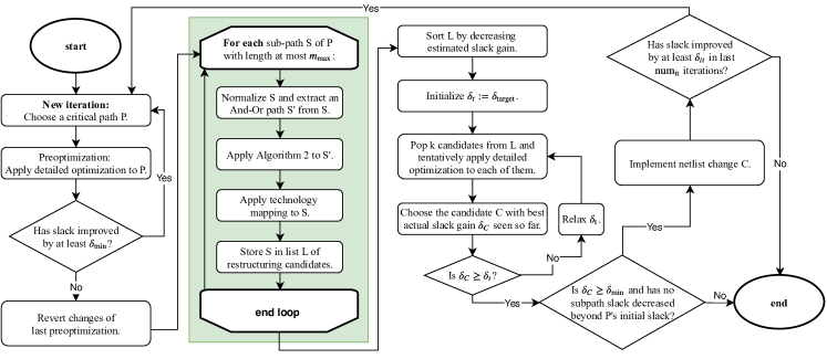
We propose a timing optimization framework (cf. figure 3) based on Werber et al. [24] with algorithm 2 as an essential component that is used in production in a late pre-routing stage of an industrial physical design flow. Our framework revises the logical structure of critical paths using placement and timing information. In section III-A, we adapt the delay model used in algorithm 2 to respect placement, buffering and gate sizing effects. As we do not fully account for different kinds of gates or different gate sizes that might be available, our framework involves a technology mapping step (section III-B) and powerful gate sizing and buffering routines (section III-C).
We iteratively optimize the worst slack of the currently most timing-critical combinational path until overall worst slack does not improve significantly anymore. A single iteration works as follows:
Let denote a most critical path. During a preoptimization step, we first try to improve the slack of without changing its logical structure in order to diminish disruptions. To this end, we apply detailed optimization to as described in section III-C. If a threshold slack improvement of is exceeded, we keep the changes imposed by preoptimization and start the next iteration.
Otherwise, we discard the preoptimization’s changes and perform the path restructuring step (central, green part of figure 3). This step works on internal data structures; the netlist is not changed before detailed optimization (section III-C). We consider the possibility to optimize any sub-path of up to a maximum length of . First, we apply a normalization (section III-A) in order to extract an And-Or path from on which we run algorithm 2. Then, the technology mapping routine from [6] (see also section III-B) locally modifies to benefit from all available gate types. After having optimized all sub-paths of , we store all restructuring possibilities in a list , sorted by decreasing estimated slack gain.
For only the most promising fraction of restructuring options, we apply the time-consuming detailed optimization (cf. section III-C). First, we tentatively apply detailed optimization to the topmost candidates in . If the actual slack gain of the best solution exceeds , we choose this solution; otherwise, we iteratively decrease by a fixed value and try out the next candidates in until we reach or is empty. Afterwards, we choose the restructuring candidate with best actual slack gain for among all detailed-optimized solutions. This way, we usually apply detailed optimization to only a few instances, but still find the overall best restructuring option. If and if no side path slack has worsened beyond the initial slack of , we implement this netlist change, possibly retaining parts of needed for side outputs. If the change is implemented and the slack gain over the last iterations exceeds a threshold , we start the next iteration; otherwise, we stop.
Note that this is a simplified flow description. E.g., in practice, we optimize the second critical path or the most critical latch-to-latch path when cannot be further optimized.
III-A Normalization
Our And-Or path optimization algorithm from section II expects as an input an alternating path of And2 and Or2 gates with prescribed input arrival times, and assumes that gates have a unit delay and connections do not impose any delay. However, the most critical path contains arbitrary gates with varying delays, and the physical locations of the path inputs might be far apart, inducing undeniably high wire delays even after buffering. A normalization step thus transforms into a piece of netlist whose core part is an And-Or path with appropriately modified input arrival times.
As we work on the most critical path, the buffering routine applied in section III-C will compute delay-optimum solutions. Thus, we can assume a linear wire delay and estimate the wire delay between two physical positions and by for a constant . The traversal time through a gate is approximated by a constant . The constants and are chosen based on an analysis of typical values on the respective design. As on the critical path, there are rather low fan-outs and slews, the delay of gates with different types and sizes still varies, but not much in comparison to the differences in arrival times. Hence, assuming a realistic constant gate delay suffices to determine the logical structure of the circuit.
Since we work on the most timing-critical part of the design, we place the circuit computed by algorithm 2 such that each path is embedded delay-optimally, implying that each path from an input to has a wire delay of , where indicates physical coordinates on the chip. Thus, the delay of is where the maximum ranges over all paths in from any input to . Applying algorithm 2 with modified arrival times
hence yields a circuit with optimum wire delay with respect to physical locations. In fact, we choose a placement that is netlength-optimum among all delay-optimum placements: We determine based on its successors in the netlist and place each gate at the median position of its predecessors and .
Now, we can describe our normalization. Let denote the most critical input of a sub-path of . We represent each gate in using and Inv gates only. This does not necessarily yield a path, but we can recover the original critical path by following the signal flow of , obtaining a path . By applying De Morgan transformations in reverse topological order, we ensure that contains and gates only, possibly adding inverters at the inputs of . We use Huffman coding (theorem 1) on chains of gates (or gates) in to move less critical gates into , respecting physical locations by modifying arrival times as above. This way, becomes an And-Or path that – with input arrival times – can be passed to algorithm 2. figure 4 depicts the normalization on a path (left) containing inverters (bubbles), Nor, and Oai gates. On the right, we show after normalization with the And-Or path colored.
III-B Technology Mapping
The purpose of our technology mapping step is to change the newly created circuit locally to improve worst slack and the physical area occupied by gates by making use of all gates available on the design. We use the dynamic programming algorithm from Elbert [6] which covers the input circuit by graphs representing the available gate types. With respect to any fixed tradeoff of arrival time (regarding our timing model from section III-A, but with specific estimated delays per gate type) and number of gates, this algorithm computes an optimum technology mapping, but the running time grows exponentially in the number of gates with more than one successor. In our application, is usually very small, hence we can effort this running time (cf. the end of section IV). For constant , [6] also provides a fully polynomial-time approximation scheme. On general circuits, computing a size-optimum technology mapping is NP-hard [12].
III-C Detailed Optimization
Depending on the actual stage of the design, our detailed optimization step invokes buffering, layer assignment and gate sizing tools. When used in late physical design, we apply Held’s gate sizing routine [9], followed by the buffering tool with an integrated layer assignment by Bartoschek et al. [2]. After buffering, we apply gate sizing again, in particular on newly inserted buffers. As we work on the most critical fraction of the design, assignment can be done conveniently by using the fastest gates available.
An incremental placement legalization makes sure that the placement remains legal throughout all netlist changes.
IV Experimental Results
In a first set of experiments, we examined the And-Or path optimization algorithm from section II separately. To this end, we created And-Or path instances with 4 to 28 inputs and random integral arrival times chosen uniformly from the interval . For each number of inputs, we created 1000 instances.
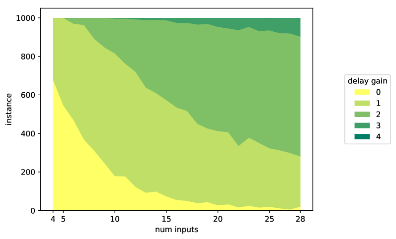
We compared our results with the previously best methods [3], [10], and [20]. For each instance, we ran all three algorithms and compared the best result in terms of delay to our algorithm’s output. figure 5 visualizes our results. Instances are grouped by their numbers of inputs, and colors indicate the absolute delay difference of computed solutions. Our algorithm covers all recursion options from [10, 3, 20], so our solutions can never be worse. In fact, on almost all instances, the delay of our circuit is better, and already for inputs, on every other instance better by or more.
For each instance, we computed a lower bound on delay based on the following ideas: First, Kraft’s inequality [15] imposes a lower bound on the delay of any binary circuit; secondly, we enumerate possible local gate configurations near the output of an And-Or path circuit and recursively compute lower bounds for sub-circuits. We compared our delay to the resulting lower bound. Among all our solutions, achieve the lower bound and hence are provably delay-optimum, and only exceed the lower bound by .
figure 6 compares our realization with [10] on an example instance. In our circuit, the splits 6∗, 7 and 7∗ were applied, and the ability to optimize undetermined circuits was used twice. This way, our delay of is better than the delay found by [10], and it is even optimum since the input with arrival time has to traverse at least gates in any solution. On this instance, we need one more gate than [10]. In general, the number of gates used by our algorithm (with our modification for size reduction) is typically higher than in [10, 3, 20], but mostly in the range of .
| Unit | Run | WS [ps] | TS [ns] | # Gates | Area | Netlength | ACE5 | T [s] |
|---|---|---|---|---|---|---|---|---|
| i1 | init | \IfDecimal201201 | \IfDecimal15.315.3 | \IfDecimal4063640636 | \IfDecimal8585 | |||
| LO | \IfDecimal188188 | \IfDecimal15.315.3 | \IfDecimal4062940629 | \IfDecimal-0.02-0.02 | \IfDecimal+0.00+0.00 | \IfDecimal8686 | \IfDecimal1212 | |
| i2 | init | \IfDecimal6262 | \IfDecimal52.252.2 | \IfDecimal6218562185 | \IfDecimal9696 | |||
| LO | \IfDecimal5858 | \IfDecimal52.352.3 | \IfDecimal6218762187 | \IfDecimal+0.02+0.02 | \IfDecimal+0.04+0.04 | \IfDecimal9696 | \IfDecimal1111 | |
| i3 | init | \IfDecimal109109 | \IfDecimal192.9192.9 | \IfDecimal6904969049 | \IfDecimal107%107% | |||
| LO | \IfDecimal9393 | \IfDecimal189.4189.4 | \IfDecimal6906669066 | \IfDecimal+0.01+0.01 | \IfDecimal+0.00+0.00 | \IfDecimal107%107% | \IfDecimal273273 | |
| i4 | init | \IfDecimal55 | \IfDecimal0.10.1 | \IfDecimal7803078030 | \IfDecimal9999 | |||
| LO | \IfDecimal00 | \IfDecimal0.00.0 | \IfDecimal7796677966 | \IfDecimal-0.06-0.06 | \IfDecimal-0.07-0.07 | \IfDecimal9999 | \IfDecimal5959 | |
| i5 | init | \IfDecimal159159 | \IfDecimal345.8345.8 | \IfDecimal210828210828 | \IfDecimal9494 | |||
| LO | \IfDecimal152152 | \IfDecimal343.4343.4 | \IfDecimal210852210852 | \IfDecimal+0.02+0.02 | \IfDecimal+0.00+0.00 | \IfDecimal9494 | \IfDecimal287287 | |
| i6 | init | \IfDecimal3434 | \IfDecimal13.013.0 | \IfDecimal264744264744 | \IfDecimal8989 | |||
| LO | \IfDecimal2020 | \IfDecimal8.58.5 | \IfDecimal264724264724 | \IfDecimal+0.00+0.00 | \IfDecimal+0.01+0.01 | \IfDecimal8888 | \IfDecimal228228 | |
| i7 | init | \IfDecimal9292 | \IfDecimal251.5251.5 | \IfDecimal272020272020 | \IfDecimal9696 | |||
| LO | \IfDecimal7777 | \IfDecimal230.1230.1 | \IfDecimal272242272242 | \IfDecimal+0.03+0.03 | \IfDecimal+0.06+0.06 | \IfDecimal9595 | \IfDecimal525525 | |
| i8 | init | \IfDecimal136136 | \IfDecimal850.1850.1 | \IfDecimal327807327807 | \IfDecimal9090 | |||
| LO | \IfDecimal120120 | \IfDecimal833.1833.1 | \IfDecimal327916327916 | \IfDecimal+0.01+0.01 | \IfDecimal+0.02+0.02 | \IfDecimal9090 | \IfDecimal249249 |
In a second set of experiments, we examined our logic optimization framework as a whole. table I shows results on recent 7nm pre-routing designs using the RICE delay model. The ’init’ row displays the state of the chips as in our application in industry: a timing-driven placement has been computed, followed by various timing optimization steps, among those our buffering and gate sizing sub-routines. The initial netlist cannot be improved any further by classical timing optimization. The ’LO’ row shows results after applying our logic optimization flow to this netlist. We see that worst slack (WS) and the total sum of negative slacks (TS) mostly improve significantly during logic optimization. This does not disrupt global objectives as area, number of gates, netlength, and routability, which barely change. To check routability, we use the ACE5 estimate from [23], the average congestion of the 5 % most congested resources, weighted by usage, computed by the global router from [18].
Our program was implemented in C++, and all tests were executed on a machine with two Intel(R) Xeon(R) CPU E5-2667 v2 processors, using a single thread. In the last column (T), we show the total running time of our flow, which is largely dominated by gate sizing because it performs many expensive queries to the timing engine. On any design, the total running time of all calls to algorithm 2 is less than second, and less than seconds for the whole path restructuring step. Per design, we consider roughly 1500 And-Or path restructuring instances with up to inputs.
V Conclusion
We presented a new approximation algorithm for delay optimization of And-Or paths and a logic optimization framework using this algorithm to improve critical paths in late physical design. Regarding a simple, but realistic delay model, our algorithm fulfills best known mathematical guarantees, outperforms previously best approaches and is often optimum. Results on industrial 7nm designs demonstrate that our logic optimization framework improves timing when traditional timing optimization tools are at an end.
References
- [1] L. Amarú, M. Soeken, P. Vuillod, J. Luo, A. Mishchenko, P.-E. Gaillardon, J. Olson, R. Brayton, and G. De Micheli. Enabling exact delay synthesis. ICCAD, pages 352–359, 2017.
- [2] C. Bartoschek, S. Held, D. Rautenbach, and J. Vygen. Fast buffering for optimizing worst slack and resource consumption in repeater trees. ISPD, pages 43–50, 2009.
- [3] U. Brenner and A. Hermann. Faster carry bit computation for adder circuits with prescribed arrival times. TALG, 15(4):45:1–45:23, 2019.
- [4] R. P. Brent and H.-T. Kung. A regular layout for parallel adders. Trans. Comput., 31(3):260–264, 1982.
- [5] J. Cortadella. Timing-driven logic bi-decomposition. TCAD, 22(6):675–685, 2003.
- [6] L. Elbert. Aproximationsalgorithmen im Technology Mapping. Bachelor’s thesis, University of Bonn, 2017. German.
- [7] M. C. Golumbic. Combinatorial merging. Trans. Comput., 25(11):1164–1167, 1976.
- [8] M. I. Grinchuk. Sharpening an upper bound on the adder and comparator depths. J. Appl. Ind. Math., 3(1):61–67, 2009.
- [9] S. Held. Gate sizing for large cell-based designs. DATE, pages 827–832, 2009.
- [10] S. Held and S. Spirkl. Fast prefix adders for non-uniform input arrival times. Algorithmica, 77(1):287–308, 2017.
- [11] D. A. Huffman. A method for the construction of minimum-redundancy codes. Proc. Inst. Radio Eng., 40(9):1098–1101, 1952.
- [12] K. Keutzer and D. Richards. Computational complexity of logic synthesis and optimization. IWLS, 1989.
- [13] V. M. Khrapchenko. Asymptotic estimation of the addition time of a parallel adder. Systems Theory Research, 19:105–122, 1970.
- [14] P. M. Kogge and H. S. Stone. A parallel algorithm for the efficient solution of a general class of recurrence equations. Trans. Comput., 100(8):786–793, 1973.
- [15] L. G. Kraft. A Device for Quantizing, Grouping, and Coding Amplitude-Modulated Pulses. PhD thesis, MIT, 1949.
- [16] J. Liu, S. Zhou, H. Zhu, and C.-K. Cheng. An algorithmic approach for generic parallel adders. ICCAD, pages 734–740, 2003.
- [17] A. Mishchenko, R. Brayton, S. Jang, and V. Kravets. Delay optimization using sop balancing. ICCAD, pages 375–382, 2011.
- [18] D. Müller, K. Radke, and J. Vygen. Faster min–max resource sharing in theory and practice. MPC, 3(1):1–35, 2011.
- [19] S. M. Plaza, I. L. Markov, and V. Bertacco. Optimizing non-monotonic interconnect using functional simuation and logic restructuring. ISPD, pages 92–102, 2008.
- [20] D. Rautenbach, C. Szegedy, and J. Werber. Delay optimization of linear depth Boolean circuits with prescribed input arrival times. JDA, 4(4):526–537, 2006.
- [21] S. Roy, M. Choudhury, R. Puri, and D. Z. Pan. Towards optimal performance-area trade-off in adders by synthesis of parallel prefix structures. TCAD, pages 1517–1530, 2014.
- [22] L. Stok, D. Kung, D. Brand, A. D. Drumm, A. J. Sullivan, L. Reddy, N. Hieter, D. J. Geiger, H. H. Chao, and P. J. Osler. BooleDozer: Logic synthesis for ASICs. IBM Journal of Research and Development, 40:407–430, 1996.
- [23] Y. Wei, C. Sze, N. Viswanathan, Z. Li, C. J. Alpert, L. Reddy, A. D. Huber, G. E. Tellez, D. Keller, and S. S. Sapatnekar. Glare: Global and local wiring aware routability evaluation. DAC, pages 768–773, 2012.
- [24] J. Werber, D. Rautenbach, and C. Szegedy. Timing optimization by restructuring long combinatorial paths. ICCAD, pages 536–543, 2007.
- [25] W.-C. Yeh and C.-W. Jen. Generalized earliest-first fast addition algorithm. Trans. Comput., pages 1233–1242, 2003.