Electronic transport in sub-micrometric channels at the LaAlO3/SrTiO3 interface
Abstract
Nanoscale channels realized at the conducting interface between LaAlO3 and SrTiO3 provide a perfect playground to explore the effect of dimensionality on the electronic properties of complex oxides. Here we compare the electric transport properties of devices realized using the AFM-writing technique and conventional photo-lithography. We find that the lateral size of the conducting paths has a strong effect on their transport behavior at low temperature. We observe a crossover from metallic to insulating regime occurring at about 50 K for channels narrower than 100 nm. The insulating upturn can be suppressed by the application of a positive backgate. We compare the behavior of nanometric constrictions in lithographically patterned channels with the result of model calculations and we conclude that the experimental observations are compatible with the physics of a quantum point contact.
I Introduction
At oxide interfaces, the interplay between confinement effects and the physical properties emerging from the junction of the constituent materials gives rise to a plethora of phenomena unattainable in III-V semiconductor heterostructures. One of the most studied systems is the conducting two dimensional electron system (2DES) appearing at the interface between LaAlO3 and SrTiO3 Ohtomo and Hwang (2004). It exhibits a series of interesting properties including gate-tunable superconductivity and spin-orbit coupling Reyren et al. (2007); Caviglia et al. (2008, 2010). Moreover, recent spin-to-charge conversion experiments, performed both in LaAlO3/SrTiO3 heterostructures and at the reduced surface of SrTiO3, evidence the potential of this interface for spintronics and topology studies Lesne et al. (2016); Chauleau et al. (2016); Song et al. (2017); Vaz et al. (2019); Trier et al. (2020).
Fundamentals to several studies and application is the capapability to reduce the lateral dimension of the conducting channels.
Among the different methods used to nanostructure the 2DES, which include photo-lithography Rakhmilevitch et al. (2010), and electron-beam lithography Stornaiuolo et al. (2012); Aurino et al. (2013); Goswami et al. (2016),
the so-called “AFM-writing” technique offers a versatile way to sketch conducting nano-devices in LaAlO3/SrTiO3 heterostructures Cen et al. (2008, 2009). It relies on the application of a positive voltage to the tip of an atomic force microscope (AFM), while scanning the LaAlO3 surface, to realize conducting patterns at the otherwise insulating interface between SrTiO3 and 3 unit cells (u.c.) of LaAlO3.
These nano-lithographic techniques give access to the study of interesting phenomena including universal conductance fluctuations Rakhmilevitch et al. (2010); Stornaiuolo et al. (2012), the Josephson effect in planar junctions Goswami et al. (2015, 2016); Monteiro et al. (2017); Stornaiuolo et al. (2017), superconductivity in AFM-written nanowires Veazey et al. (2012, 2013) and conductance quantization in quantum-point contacts (QPCs) Ron and Dagan (2014); Tomczyk et al. (2016); Thierschmann et al. (2018); Jouan et al. (2020).
Among the different phenomena recorded in these nano-devices, there are a few effects that deserve further investigation, for instance: in AFM-written nanowires it has been suggested the presence of electron pairs without superconductivity Cheng et al. (2015), and a surprisingly long ballistic length has been observed in the normal state of nano-channels Ron and Dagan (2014); Tomczyk et al. (2016). Furthermore, the role of the lithography technique on the channel properties has to be clarified, since nanowires realized via electron-beam lithography often display an insulating state at low temperature Aurino et al. (2013, 2016).
We report here on a comparative study of electric transport in (sub-)micrometric conducting channels realized at the LaAlO3/SrTiO3 interface using two methods: the AFM-writing technique and conventional photo-lithography. The lateral size of AFM-written wires ranges from 50 to 200 nm Boselli et al. (2016) and is comparable with the characteristic electronic length-scales of the 2DES at low temperature. Indeed, the inelastic scattering
length is 200 nm at 1 K Rakhmilevitch et al. (2010); Stornaiuolo et al. (2012), the elastic mean-free path ranges from 10 to 100 nm at 1.5 K Stornaiuolo et al. (2014), and the superconducting coherence length from 10 to 70 nm Reyren et al. (2007); Li et al. (2018). The temperature behavior of the channel resistance displays a clear size-dependence: wires narrower than 100 nm have a crossover from a metallic to an insulating behavior at approximately 50 K, while wider wires stay metallic down to 1.5 K.
To shed light on this effect, we also investigate devices realized by conventional photo-lithography. These paths have a minimal width of 1 m, i.e. larger than those realized via AFM-writing, but their conductance is more stable in time. One of these devices is found to have a few 50 nm wide bottle-neck constrictions giving rise to an insulating behavior below 45 K. Moreover, at 50 mK, field effect experiments revealed that the electronic transport is characterized by conductance quantization through these constrictions.
By comparing these experimental results with calculations for a quantum point contact (QPC) with a saddle-point potential, we show that the conductance quantization originates from the lateral confinement of the electrons at the interface; such lateral confinement can also explain the transport properties below 50 K.
We conclude that constrictions acting as QPCs, similar to those reported in lithographic devices, could also be at the origin of the insulating behavior observed in AFM-written nanowires.
The paper is structured as follows: the experimental methods are described in Section II and Section III presents the experimental results. Section IV describes the theoretical model developed to interpret the data, and finally we will discuss our findings in Section V.
II Experimental details
The LaAlO3 thin films have been grown by pulsed laser deposition (PLD) on commercial TiO2-terminated SrTiO3 substrates provided by Crystec GmbH, using a laser fluence of 0.6 J/cm2 and a repetition rate of 1 Hz. During the deposition, the substrates are kept at 800 ∘C in an O2 pressure of 10-4 mbar. After the deposition, the samples are annealed in-situ in an O2 pressure of 200 mbar at 550 ∘C for 1 hour, and later cooled down to room temperature in the same atmosphere. The LaAlO3 thickness, crucial for the AFM-writing technique, is monitored in-situ using the reflection high-energy electron diffraction (RHEED) technique.
After the growth, AFM-written channels are prepared (see for details reference Boselli et al. (2016)) at room temperature by scanning the AFM tip between conducting electrodes in contact with the interface. The channels’ width is controlled by the voltage applied to the AFM tip (5-9 V,) and by the number of consecutive scans, and estimated at room temperature using the so-called cutting method. They are typically 10 m long and 50 nm-200 nm wide. All the transport measurements are performed using a four-point configuration as shown in Figure 1(a).
Devices realized with photo-lithography were prepared using the following procedure: first a layer of photoresist, lithographically patterned with the shape of the conducting device, covers a bare substrate, then amorphous SrTiO3 is deposited by PLD at room temperature in an O2 pressure of 10-4 mbar, finally the photoresist is removed to expose the selected areas of the substrate to the deposition of crystalline LaAlO3.
The structures realized with this technique are Hall-bars 1 m wide and up to 300 m long (see Figure 1(d)). While their lateral size is in general larger than the characteristic electronic length-scales of the 2DES, their length/width ratio is chosen to mimic that of AFM-written wires.
For field effect tuning, we sputter a few m of gold on the backside of the SrTiO3 substrate to create a gate electrode.
III Results
Figure 1 shows the temperature dependence of the sheet resistance of four devices fabricated using the AFM-writing technique (b,c) or
patterns of amorphous SrTiO3 (e,f).
The behavior of the AFM-written wires depends on their channel width. Wires wider than 100 nm have an overall metallic behavior (see Panel 1(b)), while narrow channels have a crossover to an insulating behavior
occurring at approximately 50 K (see Panel 1(c)). This transition can be suppressed (metallicity kept down to 1.5 K) by the application of a positive voltage to the backgate (see Figure 1(c)). All the devices realized with patterns of amorphous SrTiO3 are metallic with a finite resistance at low temperature (see Figure 1(e)), except for one: a device nominally 1.5 m wide and 150 m long has a crossover from a metallic to an insulating behavior at 50 K.
A positive gate voltage restores the metallicity (see Figure 1(f)).
To understand this surprising behavior in a lithographically defined channel, similar to that of narrow AFM-written wires,

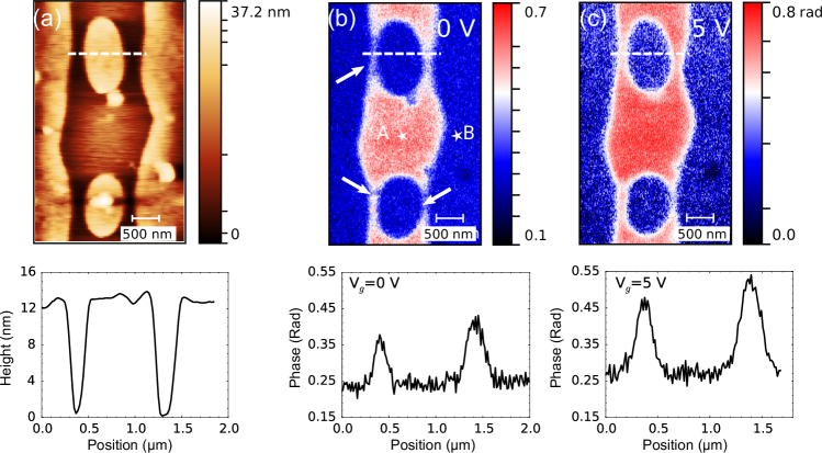
we investigated the topography of this device and revealed the presence of two consecutive oval structures located close to one end of the path (see Figure 2(a)). These regions have exactly the same height as the regions covered by the amorphous SrTiO3 used to prevent the formation of the 2DES at the interface (inset of Figure 2(a)). We believe that these islands originate from residues of photoresist left on the substrate, and we deduce that they are insulating regions creating a series of conducting constrictions 0.5-1.5 m long and from 50 to 500 nm wide in the otherwise wider conducting channel.
The 2DES conductivity in proximity to these features has been investigated using the scattering-type scanning near-field optical microscopy (s-SNOM) technique Luo et al. (2019). Figures 2(b) and (c) show two local maps, measured at 5 K, of the phase component of the s-SNOM signal. In the energy range probed here (laser wavelength of 10.7 m), the phase component of the optical response is a reliable measure of the interface local conductivity Luo et al. (2019). This analysis shows that the conductivity of the constrictions cooled down with the gate grounded is much smaller than that of the larger area of the channel.
Indeed, the s-SNOM phase difference between the center of the bottle-neck and the insulating regions around the channel, rad, is low compared to the difference referred to the wide conducting channel, rad.
By increasing the backgate voltage to 5 V, the phase difference between the constrictions and the insulating regions increases to rad, (cf. intensity of the peaks in the horizontal cuts at the bottom of Figure 2 at =0 V and =5 V), while the same quantity estimated at the center of the large channel raises to rad,
indicating that the constrictions become more metallic. These observations suggest that the insulating behavior of this device originates from the regions where the channel width is reduced.
Taking advantage of the nanosize channels created by the bottle-neck structures of amorphous SrTiO3, we measured the electronic transport below 1 K in a dilution cryostat. The sample was cooled down to 50 mK with 14 V applied to the backgate and all the measurements were performed with a constant current of 8 nA applied between the drain and the source. We note that this sample does not display any sign of superconductivity in the set-up used for the measurements. This may be related to the set-up (i.e. lack of appropriate filters or very low critical current) or to an intrinsic reason such as doping, low transition temperature or 1D behavior.
Figure 3(a) shows the resistance as a function of gate voltage at 50 mK while decreasing from to . The resistance increases from to , and, between and , it is characterized by some step-like features which are not present in wider LaAlO3/SrTiO3 paths Caviglia et al. (2008). Such a large resistance increase (by one order of magnitude) upon a gate change of a few Volts is due to the strong focusing of the electric field applied between the large gate electrode and the narrow (m wide) channel Rakhmilevitch et al. (2013). We assume that the channel resistance results from the sum of two contributions. One comes from the resistance of the wide and almost 150 m long channel, and the other from the small constrictions in series with it. We attribute the continuous increase of the resistance to the charge depletion in the full channel and the step-like features to the constrictions. This behavior is
reproducible upon several gate voltage sweeps and resembles that of the conductance of a QPC upon gate tuning van Wees et al. (1988). For a more detailed analysis, we convert the resistance data in units of quantum of conductance, () (see Figure 3(b)). shows three steps approximately high and separated by roughly .
The height of the steps is much smaller than , and this discrepancy is attributed to the contribution of the full channel to the total conductance (the wide and almost 150 m long conduction path in series with the constrictions). Therefore, a quantitative comparison with theory requires further analysis as presented in the next section.
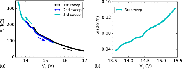
Figure 4(a) shows the constriction conductance as a function of the gate voltage at different temperatures, where four steps in are visible. These datasets have been acquired a few days after the one shown in 3(b), and the measurements are characterized by smaller noise levels and a slightly different step shape. The conductance steps survive up to 1 K, they are smeared out at higher temperature, and eventually vanish at 4 K. The suppression of the conductance quantization in temperature is expected for a QPC Akkermans and Montambaux (2007); Ihn (2010), but, interestingly, our device is particularly robust to the effect of temperature.
The application of a magnetic field (oriented out of the interface plane) induces a similar effect: the conductance steps are smeared out at 8 T as shown in Figure 4(b).

IV Numerical model
We interpret the behavior of the structural constrictions below 1 K in the framework of the saddle-point model for a QPC Büttiker (1990). The confining potential used in this approach provides a good approximation of a bottle-neck constriction as found in our lithographically-patterned device (see Figure 2(a)). It is a smooth function of the interface plane coordinates, and ( is the current direction and the transverse one), written as:
| (1) |
where is the electrostatic potential at the saddle-point, and are two frequencies related to the size of the constriction, and the electron mass. is the potential of a 2D harmonic oscillator along the axis, and a potential barrier with a parabolic shape along the axis, and can be expressed in term of the length and the width of the constriction: . By solving the eigenvalue problem relative to equation (1), one can compute the total conductance at finite temperature of a QPC using the Landauer formula Fisher and Lee (1981):
| (2) |
where is the Fermi distribution in the reservoirs, the transmission coefficient of the nth channel at energy (one should note that channel intermixing does not occur in this case as the confining potential is quadratic), the chemical potential and .
We model the experimental behavior of our device by making the assumption that the conductance jumps visible in Figure 3(b) originate from a single constriction. Equation (2) has been computed numerically, by fixing a finite number of channels entering in the sum 111We fixed the number of channels to 100. This value is large enough to describe the conductance steps observed experimentally (Figure 3(b)), involving the conduction channels at low energy. Considering a larger number of channels would imply making strong assumptions on the high energy structure of the constriction, which clearly goes beyond the regime of validity of our simple description.,
using an electron effective mass of Fête et al. (2012), and setting the chemical potential, , to zero. The position of is arbitrary as it is compensated by the value of the electrostatic potential .
We set the values of and to 35 nm and 350 nm, respectively. Despite the lack of a precise control over the geometry of our device, these values are compatible with the s-SNOM and topographic images shown in Figure 2.
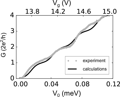
The -dependence of the calculated conductance at 50 mK is shown in Figure 5.
The energy difference, , between the conductance plateaus reflects the energy spacing between the transverse states, , the sharpness of the steps is controlled by the temperature and , and their height corresponds to a quantum of conductance, .
Considering the complex geometry of our device (see Figure 2(a)), extracting a precise value for the conductance jumps from the experimental data is challenging, as we need to estimate and remove the contribution of the full channel (the long conducting path in series with the constriction) from the total conductance (Figure 3(b)). A quite good approximation is provided by the following method.
First, we compute the resistance of the constriction, , by subtracting from the total resistance the component of the full channel (the reservoirs), computed by rescaling the total resistance to the reservoir length, , i.e.:
| (3) |
where is the total resistance of the device, and the total length of the channel (full path and constriction region). We fixed and to 147.5 m and 150 m, respectively. The value of is the nominal length of the pattern of our device, while was chosen under the assumption that the insulating islands occupy approximately 2.5 of the total channel length. Finally, from , we computed the conductance of the constriction, obtaining a value that matches steps of magnitude .
In order to compare the experimental data with the calcuations we need to estimate the scaling factor between the back-gate, , and the electrostatic potential . Indeed, these two quantities are not equivalent: while is the voltage applied to the back-electrode, is the electrostatic potential related to gate-induced Fermi energy shift. In order to convert the gate voltage into the electrostatic potential at the interface, we analyzed the effect of on a simple parabolic conduction band, with an electron effective mass of Fête et al. (2012). For a variation we computed a carrier density variation, , of . Since such is obtained in our devices by of 1.4 V Fête (2014) 222We note that this value has been extracted from analysis performed on wider devices (later size above 100 m), although the field focusing occurring in narrow ones enables to achieve the same using a lower backgate voltage Rakhmilevitch et al. (2013), we estimate a scaling factor of 1.2.
As a result of this analysis, we find a good agreement between the experimental and calculated curves (cf. Figure 5). We note that the deviations of the experimental points from the calculated curves might have multiple origins. First of all, the real geometry of the constriction might deviate from the perfectly parabolic model in Equation 1. Secondly, there might be spurious effects stemming from other constrictions present in our device (see Fig. 2).
If we extend our model to higher temperatures, we find that the calculated conductance steps are smeared out at 100 mK. Experimentally, the quantization seems to persist up to K, as visible in Figure 4(a). This could be due to a larger energy separation, , between the conductance level due to a smaller channel size. For example, if we consider a QPC with nm and nm, we find conductance steps similar to the experimental ones at 50 mK that remain essentially unchanged up to 1 K.
Therefore the real dimension of the constriction giving rise to this effect remains elusive.
While the QPC model ultimately gives reason for the insulating behavior observed in Figure 1(f), it cannot reproduce the complete behavior of the resistance in temperature, since it completely neglects a plethora of phenomena occurring at higher temperature, such as electron-phonon and electron-electron interaction, that are expected to be the dominant contribution to the resistance in this temperature range.
V Discussion
The analysis presented in the previous section shows that the conductance jumps observed in our device as a function of the back-gate result from the quantization of the transverse electronic states in a QPC. We also followed experimentally the evolution of these plateaus in temperature and magnetic field.
While the temperature dependence of the conductance quantization corresponds to what is expected for a QPC Akkermans and Montambaux (2007); Ihn (2010),
the behavior in magnetic field is less trivial to understand. The saddle-point model predicts a modification of the plateaus when a magnetic field is applied to the system, as a result of the interplay between the quantization of the energy levels induced by the confinement, , and by the magnetic field (, where is the electron charge, its mass,
and the magnetic field) Büttiker (1990). The inclusion of orbital effects in our model would lead to sharper conductance steps as the magnetic field is increased
Büttiker (1990).
In our experiments, by increasing the field to 8 T, we observe an opposite effect, since the magnetic field suppresses the conductance plateaus (see Figure 4(b)).
A recent report by Jouan et al. Jouan et al. (2020) on transport measurements in magnetic field, realized in a gate-controlled QPC at the LaAlO3/SrTiO3 interface, revealed the emergence of half-integer quantum conductance steps, 0.5(/h), at 6 T. They attribute this effect to the Zeeman splitting of the spin-degenerated QPC levels. In our system we could not observe the emergence of such additional steps. The behavior of our device might originate from additional effects of the magnetic field on the electronic reservoirs, characterized by the interplay between spin-orbit coupling, Zeeman splitting and lateral confinement provided by the lithographically defined channel, whose description goes well beyond the simplistic saddle-point model for the QPC.
The presence of quantum tunnelling barriers in conducting channels is a good candidate to explain the crossover between metallic and insulating behavior observed in our devices. In order to analyse this scenario, we used the model presented in Section IV to compute the temperature behavior of the QPC resistance for different values of the electrostatic potential (see Figure 6). Despite the limit of this calculation, that neglects any effect occurring at high temperature such as electron-phonon and electron-electron coupling, we observe that, for , the resistance of the system diverges below 30 K (Figure 6). The metallic behavior is restored only at positive values of the electrostatic potential, similarly to what we observed experimentally (see for comparison the experimental points in Figure 6).

As discussed in the experimental section, Figure 1 shows that
AFM-written wires become insulating at
temperatures which are comparable to the ones observed in the device patterned with amorphous SrTiO3 ( 40 K).
One may argue that this analogy is due to the presence of local constrictions in this electrically defined channels whose precise charge profile remains unknown. It is worth noting that, in this case, other phenomena could be equally responsible for the insulating behavior at low temperatures: the presence of multiple constrictions could act as an effective disordered potential leading to Anderson localization Anderson (1958); Abrahams et al. (1979); Lagendijk et al. (2009), a phenomenon which is robust to the presence of repulsive Coulomb interactions among electrons Giamarchi and Schulz (1988). Alternatively, the formation of consecutive barriers could lead to the formation of well isolated charge puddles acting as quantum-dots responsible for Coulomb blockade effects Aleiner et al. (2002). Further efforts in controlling the shape of thin and homogeneous wires would be important to clarify this issue.
In conclusion, this work, aiming at exploring the electric transport properties of nanoscale devices realized at the LaAlO3/SrTiO3 interface, shows that the lateral size of a conducting path has a striking effect on the resistance behavior as a function of temperature. Studying devices realized using the AFM-writing technique or with conventional photolithography, both with a lateral confinement of the 2DES lower than 100 nm, we witnessed a crossover from a metallic to an insulating behavior at 50 K. The comparison between experiments and model calculations reveals that this behavior could be understood by considering the presence of tunnel barriers acting as QPCs along the conducting path. While these findings will be useful for the interpretation of past and future experiments performed on such oxide 2D nanoscale devices, it will be of high interest studying the confinement effects in future devices, where superconductivity is present.
VI Acknowledgements
The authors wish to thank Marco Lopes and Sébastien Muller for technical support. This work was supported by the Swiss National Science Foundation through Division II (project 200020-179155), M.F by the FNS/SNF Ambizione Grant PZ00P2_174038. The research leading to these results has received funding from the European Research Council under the European Union’s Seventh Framework Program (FP7/2007-2013)/ERC Grant Agreement 319286 Q-MAC).
References
- Ohtomo and Hwang (2004) A. Ohtomo and H. Y. Hwang, Nature 427, 423 (2004), ISSN 0028-0836, URL http://www.nature.com/nature/journal/v427/n6973/full/nature02308.html.
- Reyren et al. (2007) N. Reyren, S. Thiel, A. D. Caviglia, L. F. Kourkoutis, G. Hammerl, C. Richter, C. W. Schneider, T. Kopp, A.-S. Rüetschi, D. Jaccard, et al., Science 317, 1196 (2007), ISSN 0036-8075, 1095-9203, URL http://www.sciencemag.org/content/317/5842/1196.
- Caviglia et al. (2008) A. D. Caviglia, S. Gariglio, N. Reyren, D. Jaccard, T. Schneider, M. Gabay, S. Thiel, G. Hammerl, J. Mannhart, and J.-M. Triscone, Nature 456, 624 (2008), ISSN 0028-0836, URL http://www.nature.com/nature/journal/v456/n7222/abs/nature07576.html.
- Caviglia et al. (2010) A. D. Caviglia, M. Gabay, S. Gariglio, N. Reyren, C. Cancellieri, and J.-M. Triscone, Physical Review Letters 104, 126803 (2010), URL http://link.aps.org/doi/10.1103/PhysRevLett.104.126803.
- Lesne et al. (2016) E. Lesne, Y. Fu, S. Oyarzun, J. C. Rojas-Sánchez, D. C. Vaz, H. Naganuma, G. Sicoli, J.-P. Attané, M. Jamet, E. Jacquet, et al., Nature Materials (2016), ISSN 1476-1122, URL http://www.nature.com/nmat/journal/vaop/ncurrent/full/nmat4726.html.
- Chauleau et al. (2016) J.-Y. Chauleau, M. Boselli, S. Gariglio, R. Weil, G. d. Loubens, J.-M. Triscone, and M. Viret, EPL 116, 17006 (2016), ISSN 0295-5075, 1286-4854, URL http://dx.doi.org/10.1209/0295-5075/116/17006.
- Song et al. (2017) Q. Song, H. Zhang, T. Su, W. Yuan, Y. Chen, W. Xing, J. Shi, J. Sun, and W. Han, Science Advances 3, e1602312 (2017), ISSN 2375-2548, URL http://advances.sciencemag.org/content/3/3/e1602312.
- Vaz et al. (2019) D. C. Vaz, P. Noël, A. Johansson, B. Göbel, F. Y. Bruno, G. Singh, S. McKeown-Walker, F. Trier, L. M. Vicente-Arche, A. Sander, et al., Nature Materials 18, 1187 (2019), ISSN 1476-4660, URL https://www.nature.com/articles/s41563-019-0467-4.
- Trier et al. (2020) F. Trier, D. C. Vaz, P. Bruneel, P. Noël, A. Fert, L. Vila, J.-P. Attané, A. Barthélémy, M. Gabay, H. Jaffrès, et al., Nano Letters 20, 395 (2020), ISSN 1530-6984, URL https://doi.org/10.1021/acs.nanolett.9b04079.
- Rakhmilevitch et al. (2010) D. Rakhmilevitch, M. Ben Shalom, M. Eshkol, A. Tsukernik, A. Palevski, and Y. Dagan, Physical Review B 82, 235119 (2010), URL http://link.aps.org/doi/10.1103/PhysRevB.82.235119.
- Stornaiuolo et al. (2012) D. Stornaiuolo, S. Gariglio, N. J. G. Couto, A. Fête, A. D. Caviglia, G. Seyfarth, D. Jaccard, A. F. Morpurgo, and J.-M. Triscone, Applied Physics Letters 101, 222601 (2012), ISSN 0003-6951, 1077-3118, URL http://scitation.aip.org/content/aip/journal/apl/101/22/10.1063/1.4768936.
- Aurino et al. (2013) P. P. Aurino, A. Kalabukhov, N. Tuzla, E. Olsson, T. Claeson, and D. Winkler, Applied Physics Letters 102, 201610 (2013), ISSN 0003-6951, 1077-3118, URL http://scitation.aip.org/content/aip/journal/apl/102/20/10.1063/1.4807785.
- Goswami et al. (2016) S. Goswami, E. Mulazimoglu, A. M. R. V. L. Monteiro, R. Wölbing, D. Koelle, R. Kleiner, Y. M. Blanter, L. M. K. Vandersypen, and A. D. Caviglia, Nature Nanotechnology 11, 861 (2016), ISSN 1748-3387, 1748-3395, URL http://www.nature.com/articles/nnano.2016.112.
- Cen et al. (2008) C. Cen, S. Thiel, G. Hammerl, C. W. Schneider, K. E. Andersen, C. S. Hellberg, J. Mannhart, and J. Levy, Nature Materials 7, 298 (2008), ISSN 1476-1122, URL http://www.nature.com/nmat/journal/v7/n4/abs/nmat2136.html.
- Cen et al. (2009) C. Cen, S. Thiel, J. Mannhart, and J. Levy, Science 323, 1026 (2009), ISSN 0036-8075, 1095-9203, URL http://www.sciencemag.org/content/323/5917/1026.
- Goswami et al. (2015) S. Goswami, E. Mulazimoglu, L. M. K. Vandersypen, and A. D. Caviglia, Nano Letters 15, 2627 (2015), ISSN 1530-6984, URL http://dx.doi.org/10.1021/acs.nanolett.5b00216.
- Monteiro et al. (2017) A. M. R. V. L. Monteiro, D. J. Groenendijk, N. Manca, E. Mulazimoglu, S. Goswami, Y. Blanter, L. M. K. Vandersypen, and A. D. Caviglia, Nano Letters 17, 715 (2017), ISSN 1530-6984, URL http://dx.doi.org/10.1021/acs.nanolett.6b03820.
- Stornaiuolo et al. (2017) D. Stornaiuolo, D. Massarotti, R. Di Capua, P. Lucignano, G. P. Pepe, M. Salluzzo, and F. Tafuri, Physical Review B 95, 140502 (2017), ISSN 2469-9950, 2469-9969, URL http://link.aps.org/doi/10.1103/PhysRevB.95.140502.
- Veazey et al. (2012) J. P. Veazey, G. Cheng, P. Irvin, C. Cen, D. F. Bogorin, F. Bi, M. Huang, C.-W. Bark, S. Ryu, K.-H. Cho, et al., arXiv:1210.3606 [cond-mat] (2012), URL http://arxiv.org/abs/1210.3606.
- Veazey et al. (2013) J. P. Veazey, G. Cheng, P. Irvin, C. Cen, D. F. Bogorin, F. Bi, Mengchen Huang, C.-W. Bark, S. Ryu, K.-H. Cho, et al., Nanotechnology 24, 375201 (2013), ISSN 0957-4484, URL http://stacks.iop.org/0957-4484/24/i=37/a=375201.
- Ron and Dagan (2014) A. Ron and Y. Dagan, Physical Review Letters 112, 136801 (2014), URL http://link.aps.org/doi/10.1103/PhysRevLett.112.136801.
- Tomczyk et al. (2016) M. Tomczyk, G. Cheng, H. Lee, S. Lu, A. Annadi, J. P. Veazey, M. Huang, P. Irvin, S. Ryu, C.-B. Eom, et al., Physical Review Letters 117, 096801 (2016), URL http://link.aps.org/doi/10.1103/PhysRevLett.117.096801.
- Thierschmann et al. (2018) H. Thierschmann, E. Mulazimoglu, N. Manca, S. Goswami, T. M. Klapwijk, and A. D. Caviglia, Nature Communications 9, 2276 (2018), ISSN 2041-1723, URL http://www.nature.com/articles/s41467-018-04657-z.
- Jouan et al. (2020) A. Jouan, G. Singh, E. Lesne, D. C. Vaz, M. Bibes, A. Barthélémy, C. Ulysse, D. Stornaiuolo, M. Salluzzo, S. Hurand, et al., Nature Electronics pp. 201–206 (2020), ISSN 2520-1131, URL https://www.nature.com/articles/s41928-020-0383-2.
- Cheng et al. (2015) G. Cheng, M. Tomczyk, S. Lu, J. P. Veazey, M. Huang, P. Irvin, S. Ryu, H. Lee, C.-B. Eom, C. S. Hellberg, et al., Nature 521, 196 (2015), ISSN 0028-0836, URL http://www.nature.com/nature/journal/v521/n7551/abs/nature14398.html.
- Aurino et al. (2016) P. Aurino, A. Kalabukhov, R. Borgani, D. Haviland, T. Bauch, F. Lombardi, T. Claeson, and D. Winkler, Physical Review Applied 6, 024011 (2016), ISSN 2331-7019, URL https://link.aps.org/doi/10.1103/PhysRevApplied.6.024011.
- Boselli et al. (2016) M. Boselli, D. Li, W. Liu, A. Fête, S. Gariglio, and J.-M. Triscone, Applied Physics Letters 108, 061604 (2016), ISSN 0003-6951, 1077-3118, URL http://scitation.aip.org/content/aip/journal/apl/108/6/10.1063/1.4941817.
- Stornaiuolo et al. (2014) D. Stornaiuolo, S. Gariglio, A. Fête, M. Gabay, D. Li, D. Massarotti, and J.-M. Triscone, Physical Review B 90, 235426 (2014), URL http://link.aps.org/doi/10.1103/PhysRevB.90.235426.
- Li et al. (2018) D. Li, S. Lemal, S. Gariglio, Z. Wu, A. Fête, M. Boselli, P. Ghosez, and J.-M. Triscone, Advanced Science 5, 1800242 (2018), ISSN 2198-3844, URL https://onlinelibrary.wiley.com/doi/abs/10.1002/advs.201800242.
- Luo et al. (2019) W. Luo, M. Boselli, J.-M. Poumirol, I. Ardizzone, J. Teyssier, D. van der Marel, S. Gariglio, J.-M. Triscone, and A. B. Kuzmenko, Nature Communications 10, 2774 (2019), ISSN 2041-1723, URL http://www.nature.com/articles/s41467-019-10672-5.
- Rakhmilevitch et al. (2013) D. Rakhmilevitch, I. Neder, M. B. Shalom, A. Tsukernik, M. Karpovski, Y. Dagan, and A. Palevski, Physical Review B 87, 125409 (2013), ISSN 1098-0121, 1550-235X, URL https://link.aps.org/doi/10.1103/PhysRevB.87.125409.
- van Wees et al. (1988) B. J. van Wees, H. van Houten, C. W. J. Beenakker, J. G. Williamson, L. P. Kouwenhoven, D. van der Marel, and C. T. Foxon, Physical Review Letters 60, 848 (1988), ISSN 0031-9007, URL https://link.aps.org/doi/10.1103/PhysRevLett.60.848.
- Akkermans and Montambaux (2007) E. Akkermans and G. Montambaux, Mesoscopic Physics of Electrons and Photons (Cambridge University Press, 2007).
- Ihn (2010) T. Ihn, Semiconductor Nanostructures. Quantum States and Electronic Transport (Oxford University Press, 2010).
- Büttiker (1990) M. Büttiker, Physical Review B 41, 7906 (1990), ISSN 0163-1829, 1095-3795, URL https://link.aps.org/doi/10.1103/PhysRevB.41.7906.
- Fisher and Lee (1981) D. S. Fisher and P. A. Lee, Physical Review B 23, 6851 (1981), ISSN 0163-1829, URL https://link.aps.org/doi/10.1103/PhysRevB.23.6851.
- Fête et al. (2012) A. Fête, S. Gariglio, A. D. Caviglia, J.-M. Triscone, and M. Gabay, Physical Review B 86, 201105 (2012), URL http://link.aps.org/doi/10.1103/PhysRevB.86.201105.
- Fête (2014) A. Fête, Ph.D. thesis, University of Geneva (2014).
- Anderson (1958) P. W. Anderson, Physical Review 109, 1492 (1958), ISSN 0031-899X, URL https://link.aps.org/doi/10.1103/PhysRev.109.1492.
- Abrahams et al. (1979) E. Abrahams, P. W. Anderson, D. C. Licciardello, and T. V. Ramakrishnan, Physical Review Letters 42, 673 (1979), ISSN 0031-9007, URL https://link.aps.org/doi/10.1103/PhysRevLett.42.673.
- Lagendijk et al. (2009) A. Lagendijk, B. v. Tiggelen, and D. S. Wiersma, Physics Today 62, 24 (2009), ISSN 0031-9228, URL https://physicstoday.scitation.org/doi/10.1063/1.3206091.
- Giamarchi and Schulz (1988) T. Giamarchi and H. J. Schulz, Physical Review B 37, 325 (1988), ISSN 0163-1829, URL https://link.aps.org/doi/10.1103/PhysRevB.37.325.
- Aleiner et al. (2002) I. L. Aleiner, P. W. Brouwer, and L. I. Glazman, Physics Reports 358, 309 (2002), ISSN 0370-1573, URL http://www.sciencedirect.com/science/article/pii/S0370157301000631.