Probabilistic Value-Deviation-Bounded
Source-Dependent Bit-Level
Channel Adaptation
for Approximate Communication
Abstract
Computing systems that can tolerate effects of errors in their communicated data values can trade this tolerance for improved resource efficiency. Many important applications of computing, such as embedded sensor systems, can tolerate errors that are bounded in their distribution of deviation from correctness (distortion). We present a channel adaptation technique which modulates properties of I/O channels typical in embedded sensor systems, to provide a tradeoff between I/O power dissipation and distortion of communicated data. We provide an efficient-to-compute formulation for the distribution of integer distortion accounting for the distribution of transmitted values. Using this formulation we implement our value-deviation-bounded (VDB) channel adaptation. We experimentally quantify the achieved reduction in power dissipation on a hardware prototype integrated with the required programmable channel modulation circuitry. We augment these experimental measurements with an analysis of the distributions of distortions. We show that our probabilistic VDB channel adaptation can provide up to a 2 reduction in I/O power dissipation. When synthesized for a miniature low-power FPGA intended for use in sensor interfaces, a register transfer level implementation of the channel adaptation control logic requires only 106 flip-flops and 224 4-input LUTs for implementing per-bit channel adaptation on serialized streams of 8-bit sensor data.
Index Terms:
Approximate computing, approximate communication, sensors, information theory.1 Introduction
Most computing systems are designed to prevent errors in computation, memory, and communication. Guarding against errors however requires energy, temporal redundancy, or spatial redundancy and therefore consumes resources. But not all systems need to be free of errors: In some systems, either by explicit design or by the nature of the problems they solve, system output quality degrades gracefully in the presence of errors.
Several important applications of computing systems, ranging from wearable health-monitoring systems to neuromorphic computing architectures [1] often dissipate a significant fraction of their energy moving data. For these systems the effects of errors are best quantified in terms of their integer distance, rather than using a Hamming distance. At the same time, the computations that consume this data can often tolerate errors with a wide range of integer distances with limited system-level consequences [2, 3, 4].
Because electrical communication interfaces do not benefit as much as processors and other digital logic from semiconductor process technology scaling, the fraction of system energy dissipated by sensor data accesses and sensor data movement is currently large [5, 6, 7] and will only grow in future embedded sensor-driven and neuromorphic systems. It is therefore an important challenge to find ways to reduce the power dissipated in sensor data acquisition and transfer. One way to do this is by exploiting knowledge of the properties and uses of the transported data, to reduce communication energy expenditure in exchange for, e.g., bounded inaccuracy of the communicated values [8, 9, 10, 11, 12, 13].
Reducing I/O energy usage in exchange for bounded inaccuracy requires a physical channel property that provides such a tradeoff. One example of such a tradeoff is between energy dissipated in the pull-up resistors on a serial communication interface such as I2C and the error or erasure rate. The choice of the pull-up resistor value influences signal integrity at a given I/O speed and at the same time affects communication power dissipation.
1.1 Contributions
We exploit value representation and hardware properties of communication channels to design channel adaptation techniques that trade lower power dissipation for value-bounded distortion, for a given bound on its distribution. Given a target bounding distribution, our method varies the channel bit error rates across the ordinal bit positions in a word to reduce energy used in transmission in such a way that the distribution of the resulting distortion is enclosed within the target distribution. We present a proof-of-concept hardware implementation of the technique which operates by changing properties of the I2C communication channel for individual bit positions according to provided channel adaptation specifications. We calculate these specifications at system design time to generate the appropriate channel adaptation hardware. The generated channel adaptation hardware is efficient. Because the technique we present changes the physical properties of only the channel, its implementation requires no changes to the transmitter (e.g., a sensor), easing potential adoption.
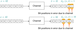
A new technique for approximate communication, probabilistic VDB bit-level channel adaptation (Section 4): In a system with integer-representing binary-valued random variable input and output , let the random variable denote the absolute value of the difference between the integers and . Figure 1 shows an example. We refer to the random variable as integer-value distortion, or just distortion. It takes on instance values and has tail distribution . We denote integer distance errors tolerated by an application using an upper bound on the tail distribution of seen at the output of the system (e.g., the receiver in Figure 1). Given any instance of the function , our method derives an application-specific per-bit channel adaptation such that for all possible distortion values . In contrast, rate distortion codes [14, 15] typically only bound the expected value of the channel distortion. To facilitate channel adaptation, we developed a computationally-efficient algorithm for calculating the distortion distribution of a given channel (i.e., given its bit-error probabilities) with given input distribution (Section 4.1). Using this algorithm, we demonstrate channel adaptation by implementing the offline search for finding optimal bit-error probabilities with bounded distortion distribution in the cases when the bit-error probabilities are identically-distributed over the bit positions and when they are non-identically distributed (Section 4.2). The latter enables bit-level channel adaptation, while the former only achieves word-level adaptation.
A case study for the proof of concept of the proposed method for the I2C communication channel (Section 5): We use pull-up resistance modulation as a means for I2C channel adaptation and experimentally verify power savings of up to 2 ( absolute saving) on a custom hardware research platform (Section 5.3). This saving in I/O power is larger than the operation power dissipation of many state-of-the-art sensors in low-power embedded systems and is therefore significant. Combining experimental measurements (Section 5.3 and Section 5.4) with a model of I2C interface circuitry (Section 5.1), we estimate circuit parameters (not always known for commercial integrated circuits) of our hardware platform (Section 5.5). We analytically derive the dependence of the bit-error probabilities of an I2C channel with given circuit parameter values on the value of the external pull-up resistance (the channel modulator). We use this analytic model to calculate the distortion distribution as a function of pull-up resistance value and identify the range of resistances for modulation to have plausible control over bit errors for reliable channel adaptation (Section 5.6).
An analysis of the hardware cost for implementing channel adaptation (Section 6): We demonstrate the feasibility of our probabilistic VDB bit-level channel adaptation technique by synthesizing the digital logic required to control the channel adaptation, targeting a small-footprint low-power sensor interface FPGA. We report the required FPGA resource usage for sensor sample resolutions common in embedded sensor systems (e.g., – bits).
1.2 Adaptation versus Source / Channel Coding
The method we present is hard to classify as a coding scheme in the conventional nomenclature of the literature. Traditional source coding changes the words transmitted on a channel to adapt to properties of the inputs (e.g., for compression). Traditional channel coding changes transmitted words to adapt to properties of the channel (e.g., for forward error correction). In contrast, the method we present (probabilistic VDB bit-level channel adaptation) takes the peculiar approach of changing the properties of the communication channel for different ordinal positions in a transmitted word in order to reduce the energy needed to transmit the data. Probabilistic VDB bit-level channel adaptation does this with the objective of reducing power dissipation by inducing channel errors that lead to values at the channel’s receiver which are at small integer distances from those sent by the channel’s transmitter. We present a detailed comparison to the related literature next, in Section 2.
2 Related Research
Value-deviation-bounded (VDB) integer codes [16] were proposed as a means of trading energy efficiency for correctness in the context of program variable encodings when program variables can tolerate some distribution of integer value distortions. For serial communication interfaces such as I2C and SPI, which are common in energy-constrained embedded systems, serial VDB codes (VDBS encoding) [10, 9] provide a concrete encoding method. VDBS encoding is deterministic and has the effect of re-quantizing the number representation of values. This deterministic distortion may be undesirable for certain applications: When applied to images with encoder settings to maximally reduce I/O energy dissipation, VDBS encoding leads to regular quantization banding in images. For these and similar applications, encoding methods that trade energy-efficiency for accuracy and whose induced distortion is stochastic are therefore desirable. Existing VDBS encoding techniques must be implemented at the data transmitter. Although, being a re-quantization, they require no decoding, their adoption requires their integration into data sources such as sensors. Because the consumers of sensor data, such as microcontrollers, provide the opportunity for programmability, a variant of VDBS encoding that could be enforced from the side of consumers of sensor data could enable widespread adoption of VDBS encoding and its benefits.
Rate distortion theory [14, 17] investigates the tradeoff of encoding efficiency (rate) for deviation of encoded values (distortion). A distortion function or distortion measure specifies this distortion as a function of the original data and its encoded form. The value deviations we consider in this work are integer distance distortions. Unlike the convention in rate distortion theory, the method we present guarantees bounds on the entire distribution of distortions, rather than only guaranteeing bounds on the expected value of the distortion.
Relation to previous probabilistic VDB methods: Prior work [8] on probabilistic VDB codes with integer value distortion adopts the same approach of trying to guarantee bounds on the entire distribution of distortions. The method we present in Section 4 builds on and improves on that work in several dimensions. First, we provide a fast method for exact calculation of the distortion distribution for the general case when bit-error probabilities may depend on the bits transmitted. This is in contrast with previous [8] work, which used an SMT solver to search for optimal bit-level channel adaptation probabilities. That method only attempts at an approximate calculation of distortion distribution by considering only up to -bit concurrent errors for -bit words transmitted. Second, we propose an alternative search algorithm through the space of bit-error probabilities, which utilizes the exact calculation method we developed. This method, besides being exact, outperforms the SMT search based on approximate constraints in terms of computation time. Third, we verify the feasibility of channel adaptation on I2C systems by carrying out a proof-of-concept implementation. We demonstrate power reduction using empirical measurements of power dissipation and carry out analytical investigation of induced channel errors to explore the design space. Fourth and finally, we demonstrate the adoptability of the approach by estimating the resource usage of the digital logic block required to control the analog channel adaptation circuitry.
| Notation | Definition | Example |
|---|---|---|
| Word length (in bits) | 8 | |
| , | Error-free binary value | 00101010 |
| , | Binary value after channel error | 00100000 |
| Number of perturbed bits, | 2 (grayed-out above) | |
| Hamming distance | ||
| Conversion from binary | (00101010) | |
| to unsigned integer | ||
| , | Error-free integer value, | (00101010) |
| Integer value after | (00100000) | |
| channel error, | ||
| , | Integer value distortion, | 10 |
| Signed error vector, | ||
| Set of all possible in words | ||
| of length | ||
| Set of all possible in words | ||
| of length with integer value | ||
| distortion | ||
| Set of all possible of length | ||
| Set of all possible that | ||
| permit a given error vector | ||
| PMF of transmitted words | ||
| PMF of transmitted | See Figure 5 | |
| integer values, | ||
| CDF of transmitted | ||
| integer values, | ||
| PMF of integer value | See Figure 2(a) | |
| distortion, | ||
| CDF of integer value | See Figure 2(b) | |
| distortion, | ||
| Constraint tail distribution | See Figure 3 | |
| Tail distribution, |
3 Definitions
Table I summarizes the notation we use in the rest of this work. Let denote the random variable with instance value , an -bit binary sequence transmitted on a channel. Let the channel output be with corresponding random variable .
We consider systems where channel inputs encode unsigned integers and we define channel errors as the absolute difference of these integer values. Let denote the ’th bit of and let denote the conversion from binary to an integer with
We define the random variable with instance values and with values . Then, we define the distance between channel input and output as
The random variable denoting values of channel distortion, with instance values , takes on values determined by the distance function , i.e., . We will use the variable when we wish to refer to specific instances of channel integer distortion and we will use when we want to emphasize the distortion function.
For each of the random variables defined, we respectively denote its probability mass function (PMF), cumulative distribution, and tail distribution by , , and with the variable as subscript, e.g., , , and . In the case of variable , for -bit words transmitted over the channel, the domain of is and we have
Finally, we define the constraint tail distribution as the distribution of integer distances which the system consuming the output of the communication channel can tolerate. has the same domain as and it may be any non-increasing function with range .
4 Probabilistic VDB Source-Dependent Bit-Level Channel Adaptation
We consider a communication channel that transmits integer data represented by -bit binary words . Suppose we have a tunable method at our disposal to induce errors in this communication channel that lets one vary the error probabilities of each bit in a controllable manner. We assume that the method of inducing errors on the channel comes with a benefit (e.g., a reduction in power dissipation) and that we have a mapping, , that quantifies the benefit for a given set of bit-level error probabilities.
Given the knowledge of bit-error probabilities and the distribution of input words to the channel, one can calculate , the PMF for the distribution of induced distortion. This is equivalent to finding the tail distribution of the induced distortion.
Given the foregoing conditions, probabilistic VDB source-dependent bit-level channel adaptation consists of finding the correct set of parameters for the mapping , i.e., the bit-error probabilities, such that: ➊ for each and ➋ the benefit is maximized. We first present our method for calculating and then present our search method for finding bit-error probabilities that satisfy conditions ➊ and ➋.
4.1 Calculating
Recall, from Table I, that is the PMF of integer value distortions that occur during transmission of -bit words. One can calculate it exactly provided that one knows the bit-error probabilities suffered during a transmission and the PMF of input words . Given these, to calculate for each , we first characterize all possible word-level error events resulting in a distortion value of . Then, for each possible input , we determine the probability of each event resulting in -distortion given is the input. The sum of all these event probabilities is equal to .
Characterization of all error events with distortion : We can identify all possible word-level error events in -bit words with the set of all error vectors of length with entries from the set of error polarities , i.e.,
where denotes the ’th entry of the error vector . If a word-level error event involves a bit-level error of 0 1, 1 0, or no error at the ’th bit, then the corresponding error vector has , , or , respectively. Let the integer value distortion corresponding to a given error vector be
Given input and output words of the channel and channel error , we have .
Let be the set of all possible error vectors causing -distortion, that is
The set characterizes all possible word-level error events with distortion . Computing requires computing the sets for each .
The computation of the sets makes use of the fact that a word-level error event is a disjoint union of its constituent bit-level error events (even if distinct bit-level events may depend on each other). An error at the ’th bit introduces a signed distortion of , - or depending on its polarity. The distortion resulting from the word-level error event is the absolute value of the sum of the signed distortions resulting from all constituent bit-level errors. In analogy to the fact that the distribution of the sum of two random variables is the convolution of their distributions, one can construct the sets all at once with an -step generalized convolution of set-valued functions.
Let and be two set-valued functions on such that for each the sets and contain elements from the same group, with group operation “”. The set-valued convolution between two set-valued functions is again a set-valued function defined by
| (1) |
where and are the summation and multiplication of sets, respectively. Given two sets
we define the sets and as
and
respectively, where stand for disjoint union. From the observation that
| (2) |
the set-valued convolution defined by (1) reduces to the standard convolution if we only consider the sizes of the sets. For a given set-valued function , if we define by
| (3) |
then
| (4) |
Coming back to the calculation of the sets , let the unit positive error vectors for each be
and consider the vector-set-valued functions defined on by
where is the empty set and is the zero error vector. For a given , encodes the possible error events at the ’th bit only according to their polarities by storing the corresponding error vector in the set labeled by the signed-integer distortion the error causes. Then, the set-valued function, defined by the -step set-valued convolution
| (5) |
encodes all possible word-level error events by storing the corresponding error vector in the set labeled by its signed-integer distortion. Consequently, we have
Determining event probabilities and finding : Once we have calculated we can calculate provided that we know the bit-level error probabilities of the channel and the occurrence probabilities of the input words. For a given input word , let and denote the probabilities of 1 0 and 0 1 erroneous bit transitions for the ’th bit given it has the correct initial value, i.e., given for negative polarity error and given for positive polarity error. A given error vector can occur only if the input word is in the set
Hence, the occurrence probability of an error vector is
| (6) |
where the probability that occurs given is
| (7) |
with
| (8) |
for .
As contains all word-level error events that cause integer value distortion of , summing the error occurrence probabilities over this set gives us the probability that the integer value distortion is . That is, we have
Using the PMF we calculate the tail distribution as
In the special case of maximal entropy input distribution we have
Assuming the individual bit-error probabilities are independent of the transmitted word (which is not the case for the I2C channel for instance, see Section 5), in view of the relations (7) and (8) and the structure of the set , the occurrence probability of given by (6) reduces to the product
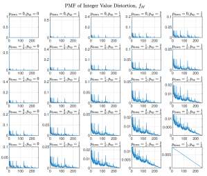
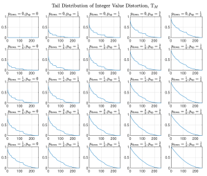
Figure 2 shows the results of the calculations carried out in the case of -bit words with maximal entropy input when the error probabilities are independent of the bit-position, i.e., for all . The plots sweep and in the range of with resolution . Figure 2 (a) and (b) respectively depict the dependencies of the probability mass function and the tail distribution on and . All plots illustrate the expected channel behavior of elevated integer value distortion with increasing bit error probabilities.
4.2 Searching for Optimal Bit-Error Probabilities
In practice, an implemented channel adaptation technique will only be able to modulate the channel to finitely many distinct states. This will yield a finite number of possible collections of bit-error probabilities for all possible words , where we define
For each such state, using the corresponding collection of bit-error probabilities, we can calculate the induced tail distribution as Section 4.1 describes. Given a benefit functional we would then select after an exhaustive search the state that yields the maximal average benefit
| (9) |
while also satisfying the constraint for all .
We demonstrate the results for the case when the word length is and assume that the input words to the channel are uniformly distributed. We also assume that the bit-error probabilities are independent of the transmitted word, i.e., for all . In this case, the average benefit defined by (9) reduces to .
We consider two sub-scenarios, first when the bit errors are independent of the bit positions, i.e., and second when they depend on the bit positions. We define the benefit functional as
| (10) |
is an increasing function of its argument. Hence, this choice of obeys the principle that the cost (e.g, error suffered) directly correlates with benefit. Searching with bit errors independent of the bit positions: In the first scenario we carry out an exhaustive search through the space of possible bit-error probabilities with a probability resolution of . Searching with bit errors dependent on the bit positions: In this scenario, the space to search through () is too large to carry out an exhaustive search with a fine probability resolution (e.g., ). Thus, we employ a search algorithm with adaptive probability resolution. Specifically, in the first step, we do an exhaustive search with the initial probability resolution of to find an optimal probability vector , that is, one that maximizes the average benefit . The probability vectors we search through have the form
where is the -vector and or for , so that the search involves probability vectors. In the subsequent steps, we continually halve the probability resolution until we reach to the probability resolution of (i.e., , ) and in the ’th step, to find that maximizes , we search through the probability vectors of the form
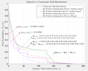
Evaluation of search methods: To generate an example constraint tail distribution , we generate a random probability vector and consider the scenario when only the is transmitted over the communication channel. In this scenario the only possible bit-errors are 0 1 errors and we assume that describes the probabilities of these errors, i.e., we take and . We set the example constraint tail distribution as the distribution of the integer value distortion suffered in this scenario. Then, for , the PMF of the suffered integer value distortion is
where is defined as in Section 3 (see Table I) and corresponds to the value of the ’th bit of the binary representation of . The example constraint tail distribution is given by
Figure 3 shows for the case when the input is uniformly distributed the constraint tail distribution together with the induced tail distributions of integer value distortion corresponding to the benefit-maximizing bit-error probabilities encountered in our search algorithms. Figure 3 also plots the tail distribution of induced integer value distortion when the bit-error probabilities satisfy . We refer to this as the oracle tail distribution, as it requires the knowledge of the random vector , which the search algorithms do not possess. The oracle tail distribution is bounded by the constraint tail distribution, because in the case of error induction with same bit-error probabilities (for both and ) when input is uniformly distributed as in the case of the constraint tail distribution scenario (where only is transmitted and only 0 1 bit-errors can occur) the induced integer value errors by distinct bit-errors may have different signs and do not compound as in the oracle scenario where distinct bit-errors always have the same sign. Finally, Figure 3 also plots the tail distribution of integer value distortion of the exhaustive search for bit position independent errors for the case when the input is always .
In the case of uniform input distribution, the results reveal that the separate control of error rates in individual bit positions allows one to induce integer value distortion on the channel with a larger corresponding average benefit than achievable by bit-position-independent error induction, as well as than that the oracle tail distribution achieves. Even though the improvement due to this capability is undetectable when induced tail distributions are visually compared, in terms of average benefit maximization the adaptive bit-dependent search algorithm achieves the largest average benefit with in arbitrary units compared to of the exhaustive bit-position independent search (more than improvement) and that the oracle tail distribution achieves. On the other hand, when only is transmitted over the channel the bit-position-independent error induction can only achieve an average benefit of compared to achievable with bit position dependent error manipulation, which is the average benefit corresponding to the probabilities of the constraint tail distribution. In general, independent of the shape of the input distribution and whether the bit errors depend on the words transmitted, it should be expected that bit-level error manipulation will achieve better performance in terms of achievable average benefit, because the set of bit-error probabilities admitted in the case of bit-position-independent error induction is a subset of the set of bit-error probabilities admitted in the case of bit-position-dependent error induction.
Finally, in comparison to the approximate method of prior work [8] for calculating the distribution of integer value distortion for given bit-error probabilities, the exact calculation method provided in this paper is more computationally efficient. This fact reflects itself in the computation time the respective search algorithms take for finding the benefit-maximizing bit-error probabilities inducing a tail distribution of integer value distortion bounded by a given constraint tail distribution. For the special case of bit-position-independent bit-error probabilities, while the method of prior work takes minutes, the method we describe in this section takes only seconds on the same workstation.
5 Case Study: Channel Adaptation on the I2C Serial Bus
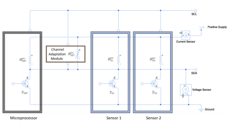
The Inter-Integrated Circuit serial bus (I2C) is a serial communication bus widely used in embedded sensor interfaces and consists of two signals: a serial clock (SCL) and a serial data line (SDA). Figure 4(a) shows how a processor (the master) can communicate with multiple sensors (the slaves) over I2C. Data transfers in I2C occur in multiples of a byte. Drivers on the I2C bus are open-drain and the I2C standard requires systems implementing it to provide pull-up resistors on both SDA and SCL. To implement the channel adaptation method of Section 4, we implement these pull-up resistors with two digitally-controlled potentiometers (DCPs). Because of the pull-up resistors, when the I2C bus is idle, both SDA and SCL voltages are close to the I/O supply voltage. To pull SDA or SCL low, either the master or the slave sinks the current through its drive transistor to ground.
5.1 I2C Electrical Parameters
Typically, designers choose a significantly larger value for the pull-up resistance compared to the on-resistance of the transistor in order to achieve logic-0 voltage close to zero. Furthermore, for the bus to be able to charge/discharge to these voltage levels within an I2C clock cycle one requires the charging/discharging time constants of the I2C data bus and to be comparably small. As transistors with both very small on- and very large off-resistances are available, choosing small enough to be able to charge the bus in time is the main constraint determining its value from the perspective of reliable transmission. On the other hand, the main source of power dissipation in I2C data transmission is due to current flow through during a logic 0 transmission. Consequently, during transmission, using values of higher than those used for reliable operation will reduce reliability, but it will also reduce power dissipation.
Reduction in transmission reliability corresponds to an increase in bit-error probabilities, whereas reduction in power dissipation corresponds to an increase in power savings. Accordingly, the benefit functional defined in Section 4, which takes the bit-error probabilities as input and whose value translates to power savings within the I2C channel adaptation framework, should be an increasing function of its arguments. The definition (10) in Section 4.2 obeys this principle.
5.2 Implementing Bit-Level Channel Adaptation for I2C
We implement source-dependent bit-level channel adaptation for the I2C channel, establishing a tradeoff between transmission reliability and power dissipation by manipulating the value of the pull-up resistance during each bit transmission of an I2C transaction. Here, we focus on the analog electrical behavior of the bus for different per-bit values of the pull-up resistance achieved by the combination of digital modulator logic and the variable resistor. We present the digital logic for controlling the DCP in Section 6.
The channel adaptation module in Figure 4(a) takes as input the I2C SCL and SDA lines and modulates the value of the pull-up resistor on a per-bit-clock basis. For each sensor on the I2C channel that transmits data in chunks of bits, the channel adaptation module contains offline-calculated pull-up resistance selections corresponding to resistances , which will lead to associated bit error probabilities that are permissible for that bit position (calculated in Section 4). The channel adaptation module synchronizes with the I2C transaction and switches the pull-up resistance to at the beginning of transmission of the ’th bit of each data chunk of size , . The switching of the pull-up resistances on a per-bit-clock basis requires the channel adaptation module to switch the DCP at a frequency much higher than the clock frequency of the I2C transaction, which may go up to MHz (referred to as the ultra-fast mode). On the other hand, the CMOS switches on a typical application-specific integrated circuit with a nm process can switch their output in ps and can do so every ns, which permits bit-level channel adaptation even for ultra-fast mode I2C transactions with the pull-up resistance switching occupying less than of an I2C clock cycle.


The user input of our method is the expected sensor data distribution and an upper bound tail distribution on the permitted integer value distortion. Figure 5 shows an example of real-world distributions of the error-free integer values (see Section 3). Using these inputs in an offline step performed at system design time, we derive a specification of pull-up resistance selections. The resulting communication on the I2C bit-level-adapted channel which switches pull-up resistance according to this specification yields a tail distribution of integer value distortion globally bounded by . The resulting approximate channel consumes less power than the unadapted channel.
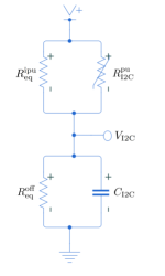
To be able to find optimal pull-up resistance values for I2C channel adaptation given the input distribution and user-defined bound on distortion distribution and to estimate the resulting power savings, we need to characterize the dependence of power dissipation and induced distortion distribution on pull-up resistance value. We measure the power dissipation dependence experimentally. This also lets us estimate the parameters of the equivalent circuit around the I2C data bus during reception of logic 1 provided in Figure 4 (b). For the dependence of integer value distortion incurred during transmission we present an analytic model in Section 5.6.
5.3 Setup for Measuring the I2C Power Dissipation Dependence on Pull-up Resistance
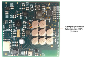
To determine the dependence of I2C bus power dissipation on the value of the pull-up resistor, we ran experiments on the I2C communication interface in Warp [19], an open-source hardware platform for research into tradeoffs between accuracy and power dissipation (see Figure 6).
We use two ISL23415 DCPs [20] as configurable pull-up resistors on the SDA and SCL lines of the I2C bus. The ISL23415 is an integrated circuit that occupies an area of less than . It dissipates less than of power over its CMOS switches when switching between different resistance settings. Because we cannot control the ISL23415 DCPs to switch resistance values between I2C clock cycles, we use them primarily to demonstrate the feasibility and potential power savings for the case where we use the same pull-up resistance value for all clock cycles. A custom integrated circuit combining the digital interface from Section 6 with the internals of a device such as the ISL23415 would be primarily an engineering task and would not provide much additional research insight.
We measured the dependence of I2C bus power dissipation on the pull-up resistance at . We selected , , , , and as pull-up resistance values for investigation. The lowest value is in the range of typical external I2C pull-up resistance values.
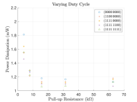
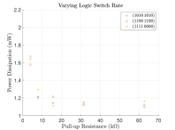
We used an MMA8451Q digital accelerometer [21] as the target sensor in our measurements. To control the bytes transmitted by the sensor over the I2C bus, we write a prescribed value to a sensor configuration register and request the sensor to send that value back times. We used two sets of bytes to characterize the power dissipation on the I2C bus. The first set (0000 0000, 1100 0000, 1111 0000, 1111 1100, 1111 1111) has bytes with varying duty cycles of logic 0 and 1 and have fixed logic switch frequency. The second set of bytes (1010 1010, 1100 1100, 1111 0000) all have equal duty cycles for both logic values but have varying number of transitions between logic states.
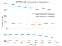
We use a Keithley SMU2450 6.5-digit laboratory source-measure unit with a current measurement resolution of 10 nA to power the Warp and determine the power consumed by I2C communication by measuring the current drawn by the power supply. Figure 7(a) shows raw current measurement data at the lowest and highest DCP settings. Each data point corresponds to a current measurement. The first five high current plateaus correspond (in order) to transmissions of the five bytes in the first set given above and the last two correspond (in order) to the first two bytes in the second set.
From the raw current data we estimate average current consumption during repeated I2C transmissions of a given byte by taking the difference between the averages of data points on the plateau and the averages of points around it (four on each side). We then find the average power consumption by multiplying the average current consumed by the positive supply voltage, which we set to in the experiment.
5.4 Measurements Results
Figure 7(b) and (c) show the dependence of I2C power consumption on the I2C pull-up resistance value for transmitted bytes with varying duty cycles (and fixed logic switch frequency) and with varying logic switch frequency (and fixed duty cycle), respectively. The results show a clear inverse dependence of the I2C power dissipation on the pull-up resistance value with an absolute value of power savings of up to . The power dissipation, which can be as high as for the lowest used resistance value of (typically used in practice), reduces below and settles to a plateau above , implying up to 2 power reduction. The reason for this plateau is the existence of the internal pull-up pathways embedded into sensors and/or processors as Figure 4 shows. Furthermore, the results confirm the expected behavior of increasing power consumption with increasing duty cycle of logic 0 and reveal the increasing power consumption with increasing logic switch frequency.
Because our experimental procedure involved a repetitive register read request of a fixed byte from a sensor register, the actual reading process was only a portion of the total I2C transaction. As a result, the observed differences in current measurements only reflect changes in power dissipation due to the transmission of a prefixed byte during that portion of the whole process. Consequently, observed power consumption dependencies in Figure 7(b) and (c) are less than what would be in a real-word usage scenario, where a sensor transmits streams of uninterrupted data.
5.5 Estimation of I2C High-Logic-Reception Channel Model Parameters
Both the analysis of I2C circuitry (shown in Figure 4(a)) and the experimental results indicate that one can decrease the power consumption of I2C communication by increasing the pull-up resistance of the I2C data bus. Similarly, it follows that an increase in pull-up resistance will only have detrimental effects on the transmission fidelity of high logic values. Specifically, it results in a decrease of the steady-state logic 1 I2C voltage level (bringing it closer to threshold) and in an increase of 0-to-1 transition time (risking reaching to steady-state level in an I2C clock cycle). In stark contrast, an increase in pull-up resistance causes a decrease of the steady-state logic 0 I2C voltage level (taking it further away from threshold) and a decrease of 1-to-0 transition time. Based on this observation, which we also verified with measurements provided below, the potential of our proposed method lies in the analysis of logic 1 transmission.
We evaluated the two extreme configurations of the pull-up DCP by measuring the steady-state logic 0/1 voltage levels and , as well as the rise/fall times (–) of the I2C voltage, for the minimum () and maximum () DCP pull-up resistance configurations, respectively.
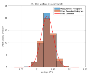
Figure 8 plots the distribution of the steady state voltage measurements of the I2C bus with the minimum DCP pull-up resistance configuration at supply voltage , together with the fitted Gaussian distribution with the same mean and standard deviation as the measurement data and the density histogram of samples drawn from the fitted Gaussian. Even though the plot visually confirms that the density histogram of the measured steady-state voltage of the I2C bus is close to the density histogram of samples drawn from the fitted Gaussian, the two-sample Cramér-von Mises test rejects the null hypothesis that the measurement data is distributed as the samples drawn from the fitted Gaussian at the level. Measurements yielded the following means and standard deviations for the low and high logic voltage levels of the I2C bus with the minimum and maximum DCP pull-up resistance configurations:
and rise/fall times
These results verify the previous hypothesis that increasing pull-up resistance increases the rise time and decreases the fall time of the I2C bus voltage.
We denote the equivalent resistance of the pull-up branch in Figure 4(b) when the DCP is in minimum/maximum pull-up resistance configuration by
is the equivalent resistance for the internal pull-up paths (connected to the supply in parallel) of all devices on the I2C bus. The resistance in the pull-down path of the equivalent circuit in Figure 4(b) is the equivalent resistance for the off-resistances of the internal transistors in the pull-down path (connected to the ground in parallel) of all devices on I2C bus.
The steady-state voltage level measurements provided above let us estimate all the resistances in Figure 4(b). In particular,
| (11) |
There are two equalities in (11). Taking the ratio of these equalities and plugging in the steady state voltage values gives
With the knowledge of the DCP pull-up resistance values this ratio yields an equivalent internal pull-up resistance of , which in turn yields an equivalent transistor off-resistance of .
After estimating the resistance values we can estimate using the rise/fall time measurements and the analytic solution of the voltage on the I2C data bus,
| (12) |
where and . Using this equation we estimate the I2C capacitance of our system as .
5.6 Analytic Derivation of Dependence of I2C Channel Integer Value Distortion on Pull-up Resistance
During bit reception process over I2C from a sensor, the sensor sets the voltage of the I2C bus at the beginning of an I2C clock cycle (when the I2C clock SCL is low), either pulling the SDA voltage down to logic 0 or letting the supply pull the SDA voltage up. We assume that an erroneous bit read from a sensor on I2C occurs when the I2C voltage sampled by the microprocessor at the end of the clock cycle (during the high-to-low transition of SCL) is on the wrong side of the threshold voltage . We take it to be half of the supply voltage, i.e., . The possible causes for such an event can be long transition times between logic levels compared to the I2C clock period and logic levels which are on the wrong side of , possibly due to noise.
Let denote the equivalent resistance on the total pull-up path in the equivalent circuit in Figure 4(b) when the DCP is at the ’th setting. The ISL23415 DCP we use in the experiments of Section 5.4 has 256 programmable levels, so . Let be the corresponding steady-state logic 0/1 voltage levels on the I2C bus and let be the corresponding rise time constant. Let denote the DCP setting values for the pull-up resistances we switch through during transmission of each integer-encoding byte, where corresponds to the first bit of the byte sent over I2C. This bit is the least or most significant bit of the byte if the sensor transmits data in little- or big-endian fashion, respectively. Also, let be the nominal index for the DCP setting with corresponding equivalent pull-up resistance yielding reliable operation without any read errors. We assume that the DCP module switches to this resistance for operation-critical bus transactions, e.g., during transmission of START/STOP or ACK/NACK, and bytes which are not integer-encoded or which cannot tolerate non-zero integer value distortion.
During data reception on I2C from a sensor, the sensor sequentially transmits sensor data in chunks of bytes. During the clock cycle, just before each such byte transmission, SDA is always low. Either the sensor sets it low just before the transmission of the initial byte as an acknowledgement (ACK) to the read request from the microprocessor or the master sets it low as an ACK in between two consecutive bytes the sensor transmits. Since logic 0 transmission on I2C is always reliable, at the beginning of transmission of each integer-encoding byte the SDA voltage will be steady at .
For and a given byte sent over the I2C bus let denote the value of transmitted bit (in time). In the I2C protocol the most significant bit is transmitted first, so that with the notation introduced in Section 3 we have . We find the probabilities of erroneous bit reception during transmission of given the DCP configuration profile via the following iterative calculations.
Assuming that the transmission of occurs during the time interval and that the initial I2C voltage at time is , iteratively on we solve an equation similar to the Equation (12) over the time interval to find . If , then transitions are rapid and I2C voltage reaches steady-state level before the end of clock cycle, so that at the end of the ’th cycle we set the I2C voltage to be . If however, then transitions are slow and we calculate the voltage levels at the end of each clock cycle as
We take the I2C voltage levels at the end of each I2C clock cycle to be Gaussian distributed (see Figure 8) with mean and standard deviation , . Then, given , the probability that the receiver erroneously perceives it as logic 0 is
After appropriate relabeling of indices (from to ) the transmitted-byte-dependent error probabilities of Equation (8) in Section 4.1 read
and
Finally, using these probabilities we calculate the distribution of the integer value distortion of the channel with the given DCP configuration profile as described in Section 4.1.
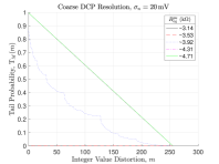
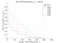
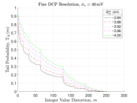
Figure 9 shows the dependence of the tail distribution of integer value distortion on the equivalent I2C pull-up resistance values in the case of uniform input distribution. Each plot corresponds to a DCP configuration profile with a fixed resistance across a whole byte. The fixed resistances correspond to the DCP settings used in power measurement experiments of Section 5.3. We choose the channel parameters same as the values estimated for our system in Section 5.5 with the exception of the bus capacitance, which we set equal to , more representative of an embedded system with fewer sensors connected to the I2C bus than in the Warp experimental system described in Section 5.3. We assume devices on I2C have no internal pull-up paths, so that the external DCP pull-up dominates the pull-up resistance.
Figure 9(a) shows the distribution of induced integer value distortion for the DCP (ISL23415TFUZ) on the Warp system used in the power dissipation experiments described in Section 5.3. The resolution () of the ISL23415TFUZ () was too coarse to have the desired accuracy of I2C error manipulation. Resistance values corresponding to consecutive DCP settings (–) yielded big jumps in the error performance of the I2C channel. However, Warp also supports the DCP ISL23415WFUZ (), which is pin compatible with the ISL23415TFUZ and has finer resolution. Figures 9(b) and (c) demonstrate the improved control on the I2C error one can achieve when using the ISL23415WFUZ as the choice of the DCP. There is no fundamental reason for not using a DCP with an even smaller granularity in a custom silicon implementation.
Figures 9(b) and (c) also demonstrate the sensitivity of the behavior of I2C error to the I2C noise levels. Figure 9(b) shows results of calculations for I2C voltage noise standard deviation , whereas Figure 9(c) shows results for . As expected, increased noise deteriorates the control over the I2C error and shifts the tail distribution of integer value distortion of the channel upwards. Thus, control of the induced I2C channel errors requires one to monitor the noise levels on I2C bus and compensate for changes in noise levels. Because primarily 1 0 errors can occur as a direct result of increasing pull-up resistor value, I2C channel errors result in received values that are numerically smaller than the actual value transmitted and the integer value distortion (which by definition is nonnegative) shown in Figure 9 correspond to negative errors only.
6 Hardware Overheads of Channel Adaptation
In Section 5 we implemented channel adaptation to I2C via a DCP module. In general, channel adaptation applies to any binary channel that transmits integer data and will require a channel adaptation module similar to the DCP module for each such channel. In this section we estimate the hardware cost of the channel adaptation module that is independent of the channel communication protocol for serial communication channels such as I2C and SPI, which are widely used in embedded systems.
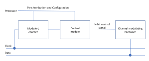
Utilization of bit-level channel adaptation exhibits a number of technical complications from the processor side, such as the operational load introduced to the processor, its accompanying power consumption and the difficulty in implementation from the timing perspective. However, these are straightforward to mitigate by providing a channel adaptation module that acts as the glue logic between the processor and the channel modulating hardware, e.g., the DCP module in the case of I2C communication discussed in Section 5.
Figure 10 illustrates a block diagram for the architecture of such a channel adaptation module. For a single sensor transmitting -bit words on a serial channel, -bit registers (1 register for each bit position and 1 for default value) suffice to store a bit-level channel adaptation configuration, which consists of selection values to choose from the possible states the channel modulating hardware can assume. The approach of feeding these values constantly through the CPU is energy inefficient and does not meet the the timing requirements of bit-level adaptation. To control the channel modulating hardware we propose a minimal control module implemented in a miniature low-power FPGA, which can be easily integrated, for instance, into existing DCP designs. The module receives from the processor the channel adaptation lookup table only once and executes adaptation when instructed. This enables fast and low-power switching of the channel modulating hardware and facilitates bit-level adaptation of high-frequency serial communication channels.
To quantify the hardware footprint of the protocol-agnostic part of the channel adaptation module, we implement its control logic in an FPGA using the Verilog hardware description language. Algorithm 1 encapsulates our implementation. We design the hardware module as a two-state finite state machine that modulates the communication channel at each negative edge of the transmission clock during data transaction. During the transmission of the ’th bit of a word, the module modulates the channel according to the selection specified by register .
We have synthesized the Verilog implementation on an iCE40 FPGA for word lengths . The synthesis revealed that, the protocol-agnostic part of the synchronization logic for the channel adaptation module utilizes carry logic, negative edge clock D flip-flops, negative edge clock D flip-flops with clock enable and -input LUTs.
7 Conclusions
We present a new communication channel adaptation technique that trades integer distance in induced errors for lower power usage. The technique achieves this by modulating the channel to vary the bit-error rate across the ordinal bit positions in a word to reduce power dissipation. To predict channel parameters, it utilizes an efficient method for calculating the exact distribution of integer value distortion suffered during bit-level adaptation. We carry out a case study for implementation of the technique on I2C channel. We empirically verify power reduction of up to 2 () by means of modulating the pull-up resistance of the I2C bus of the Warp hardware platform. We explore the design space and feasibility of the proposed scheme utilizing the developed theoretical tools for calculating the integer value distortion distribution and analytical derivations of I2C channel errors. Results indicate the need for noise compensation for reliable channel adaptation. Finally, by means of synthesizing in FPGA the protocol-agnostic part of bit-level synchronization to serial communication channels, we give an estimate for the footprint of a channel modulation hardware for sensor sample resolutions common in embedded sensor systems (e.g., – bits).
Acknowledgments
This research is supported by an Alan Turing Institute award TU/B/000096 under EPSRC grant EP/N510129/1, and by Royal Society grant RG170136. We thank Richard Hopper for assisting with power dissipation measurements in Section 5, Srisht Fateh Singh for help with the FPGA synthesis in Section 6, and James Meech, Nathaniel Tye, Chatura Samarakoon, and Vasileios Tsoutsouras for providing feedback on the manuscript.
References
- [1] P. A. Merolla, J. V. Arthur, R. Alvarez-Icaza, A. S. Cassidy, J. Sawada, F. Akopyan, B. L. Jackson, N. Imam, C. Guo, Y. Nakamura et al., “A million spiking-neuron integrated circuit with a scalable communication network and interface,” Science, vol. 345, no. 6197, pp. 668–673, 2014.
- [2] M. Shafique, R. Hafiz, S. Rehman, W. El-Harouni, and J. Henkel, “Cross-layer approximate computing: From logic to architectures,” in Proceedings of the 53rd Annual Design Automation Conference, 2016, pp. 1–6.
- [3] P. Stanley-Marbell, A. Alaghi, M. Carbin, E. Darulova, L. Dolecek, A. Gerstlauer, G. Gillani, D. Jevdjic, T. Moreau, M. Cacciotti et al., “Exploiting errors for efficiency: A survey from circuits to algorithms,” arXiv preprint arXiv:1809.05859, 2018.
- [4] P. Stanley-Marbell, V. Estellers, and M. Rinard, “Crayon: Saving power through shape and color approximation on next-generation displays,” in Proceedings of the Eleventh European Conference on Computer Systems, ser. EuroSys ’16. New York, NY, USA: Association for Computing Machinery, 2016.
- [5] H. Hatamkhani, F. Lambrecht, V. Stojanovic, and C.-K. K. Yang, “Power-centric design of high-speed i/os,” in Proceedings of the 43rd annual Design Automation Conference. ACM, 2006, pp. 867–872.
- [6] F. O’Mahony, G. Balamurugan, J. E. Jaussi, J. Kennedy, M. Mansuri, S. Shekhar, and B. Casper, “The future of electrical i/o for microprocessors,” in 2009 International Symposium on VLSI Design, Automation and Test. IEEE, 2009, pp. 31–34.
- [7] K. T. Malladi, B. C. Lee, F. A. Nothaft, C. Kozyrakis, K. Periyathambi, and M. Horowitz, “Towards energy-proportional datacenter memory with mobile dram,” in Proceedings of the 39th Annual International Symposium on Computer Architecture, ser. ISCA ’12, 2012, pp. 37–48.
- [8] P. Stanley-Marbell and P. Hurley, “Probabilistic value-deviation-bounded integer codes for approximate communication,” arXiv preprint arXiv:1804.02317, 2018.
- [9] P. Stanley-Marbell and M. Rinard, “Reducing serial i/o power in error-tolerant applications by efficient lossy encoding,” in Proceedings of the 53rd Annual Design Automation Conference, ser. DAC ’16. New York, NY, USA: ACM, 2016, pp. 62:1–62:6.
- [10] ——, “Efficiency limits for value-deviation-bounded approximate communication,” IEEE Embedded Systems Letters, vol. 7, no. 4, pp. 109–112, 2015.
- [11] Y. Kim, S. Behroozi, V. Raghunathan, and A. Raghunathan, “Axserbus: A quality-configurable approximate serial bus for energy-efficient sensing,” in 2017 IEEE/ACM International Symposium on Low Power Electronics and Design (ISLPED). IEEE, 2017, pp. 1–6.
- [12] P. Stanley-Marbell, P. A. Francese, and M. Rinard, “Encoder logic for reducing serial i/o power in sensors and sensor hubs,” in Hot Chips 28 Symposium (HCS). IEEE, 2016, pp. 1–2.
- [13] C.-H. Huang, Y. Li, and L. Dolecek, “Acoco: Adaptive coding for approximate computing on faulty memories,” IEEE Transactions on Communications, vol. 63, no. 12, pp. 4615–4628, 2015.
- [14] C. E. Shannon, “Coding theorems for a discrete source with a fidelity criterion,” IRE National Convention Record, vol. 7, no. 4, pp. 142–163, 1959.
- [15] T. M. Cover and J. A. Thomas, Elements of information theory. John Wiley & Sons, 2012.
- [16] P. Stanley-Marbell, “Encoding efficiency of digital number representations under deviation constraints,” in IEEE Information Theory Workshop, (ITW’09), Oct 2009, pp. 203–207.
- [17] C. E. Shannon and W. Weaver, The Mathematical Theory of Communication. Urbana, Illinois: University of Illinois Press, 1963.
- [18] J. R. Kwapisz, G. M. Weiss, and S. A. Moore, “Activity recognition using cell phone accelerometers,” ACM SigKDD Explorations Newsletter, vol. 12, no. 2, pp. 74–82, 2011.
- [19] P. Stanley-Marbell and M. Rinard, “Warp: A hardware platform for efficient multi-modal sensing with adaptive approximation,” IEEE Micro, vol. 40, no. 1, pp. 57–66, Jan 2020.
- [20] ISL23415 - Single, Low Voltage Digitally Controlled Potentiometer, Renesas Electronics, 9 2015, rev. 2.00.
- [21] MMA8451Q, 3-axis, 14-bit/8-bit digital accelerometer, NXP Semiconductors, 2 2017, rev. 10.3.