Email: ]ycma@tjut.edu.cn
The electric pulses induced multi-resistance states in the hysteresis temperature range of 1T-TaS2 and 1T-TaS1.6Se0.4
Abstract
The electric pulses induced responses of 1T-TaS2 and 1T-TaS1.6Se0.4 crystals in the commensurate charge-density-wave phase in hysteresis temperature range have been investigated. We observed that abrupt multi steps of the resistance excited by electric pulses at a fixed temperature forming multi meta-stable like states. We propose that the response of the system corresponds to the rearrangements of the textures of CCDW domains, and the multi-resistance states or the nonvolatile resistance properties excited simply by electric pulses have profound significance for the explorations of solid-state devices.
pacs:
71.27.+a, 71.45.Lr, 71.30.+hSolid-state electronic devices (SSED) attract much attention in scientific research and industry fields, e.g. relays, memories, batteries and switches, for their high endurance, low noise and space saving when compared to mechanical ones. In order to improve functionalities, great efforts were made to understand correlated-electron systems Imada . Under external electric fields of intense laser pulses or high electrical currents, correlated electrons can exhibit anomalous nonlinear response in transition metal compounds Yoshida ; Hollander ; Vaskivskyi ; Vaskivskyi2 , and more interesting, in some systems the current-induced state can be maintained when the electric field or the pulse is turned off. Such ‵nonvolatile′ behavior of the electrically induced switching is highly desired for data-storage applications. Of high interest is control of multi resistance states between OFF [high resistance (HR)] and ON [low resistance (LR)] by electric pulses Kim ; Huang ; Prakash ; Nian ; Rozenberg .
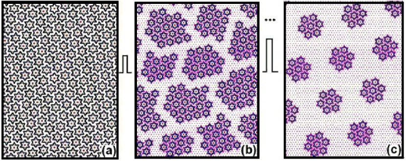
1T-TaS2 is one of the classical layered transition-metal dichalcogenides, which capture high interest in recent years: the ultra-fast resistance switching Stojchevska ; Vaskivskyi , the supercooled nearly commensurate charge-density-wave (CDW) phase Yoshida , photosensitivity from visible to terahertz at room temperature DongWu , electrically driven reversible insulator-metal phase transition Yoshida ; Hollander ; Ritschel . At room temperature, 1T-TaS2 hosts the nearly commensurate (NC) CDW. Scanning tunnelling microscopy has revealed that the NCCDW phase consists of trigonally packed CCDW domains separated by metallic regions that are not fully distorted Thomson . With decreasing temperature, a commensurate (C) CDW phase appears below 180 K, whereas in heating the CCDW state is stable up to 220 K, exhibiting remarkable hysteretic characteristics in various temperature dependent properties Yongchang_2019 ; DiSalvo ; Wilson ; Dardel ; Gasparov ; Tsen .
Because of the close energy proximity of the various competing charge ordered phases, several external perturbations or excitations can effectively modulate the CCDW phase Stojchevska ; Yoshida ; Sipos ; Yu ; Ludwiczak . These include sample dimensions, doping, thermal history, photo excitation, electric field and pressure, raising interesting questions about the dynamics especially near the phase transitions. In thin flake devices, the current induced effects were discovered on the order of kilovolts per centimeter Yoshida ; Hollander ; Tsen . However, in hysteresis region of the dc transport properties for macroscopic specimens, electric pulses with field strength of several tens of V/cm can induce persistent meta-stable states, suggested to be a mixture of the high- and low-resistance components in bulk 1T-TaS2 Yongchang_2019 . Clearly, there should exist many different meta-stable or mixture states caused by the current-induced modification of the patterns of CCDW domains. Further, as Se substitution shows a widened hysteretic temperature range (140 - 260 K) in charge transport properties DiSalvo ; Endo , one would expect that the multi meta-stable states or the nonvolatile resistance properties can be used close to room temperature. Consequently, investigations of the nonvolatile resistance states excited simply by electric pulses may have significance for solid-state rheostats to substitute the rotary or linear types and preset resistors, which are operated mechanically and manually.
In this article, we systematically investigated the electric pulses induced responses of the CCDW phase of 1T-TaS2 and 1T-TaS1.6Se0.4 in the hysteresis temperature range. The pulses could drive each of layered dichalcogenides to multi-resistance states and maintain the values until the next electric pulse, exhibiting nonvolatile resistance properties. The hysteresis region of 1T-TaS1.6Se0.4 is remarkably larger than the pristine 1T-TaS2, and thus widens the temperature scope for potential usage of the electronic devices. We propose a model to explain the emergence of the nonvolatile resistance behavior activated electrically.
The growth of 1T-TaS2 and 1T-TaS1.6Se0.4 single crystals could be found elsewhere DiSalvo ; Yongchang . In our experiments, we focused on the in-plane transport properties of the sample with surface area mm2 and thickness (along c-axis) about 30 m, and the distance between the two potential electrodes is about 0.80 mm. After the sample was transfered on a sapphire substrate, it was fixed mechanically and connected electrically by silver paint. In the CCDW state, the contact resistance is less than 1% of the bulk resistance (50 100 Ohm), providing reliable measurement results. The experimental temperature were monitored by a Cryocon 32 controller with stability better than 0.01 K. To avoid Joule heating, an electric single pulse with the duration of 40 s was applied on the specimen, followed by the resistance measurement though a dc current = 0.2 mA using a Keithley 2400 source meter. Similar experimental data were reproduced well for other samples.
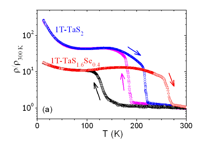
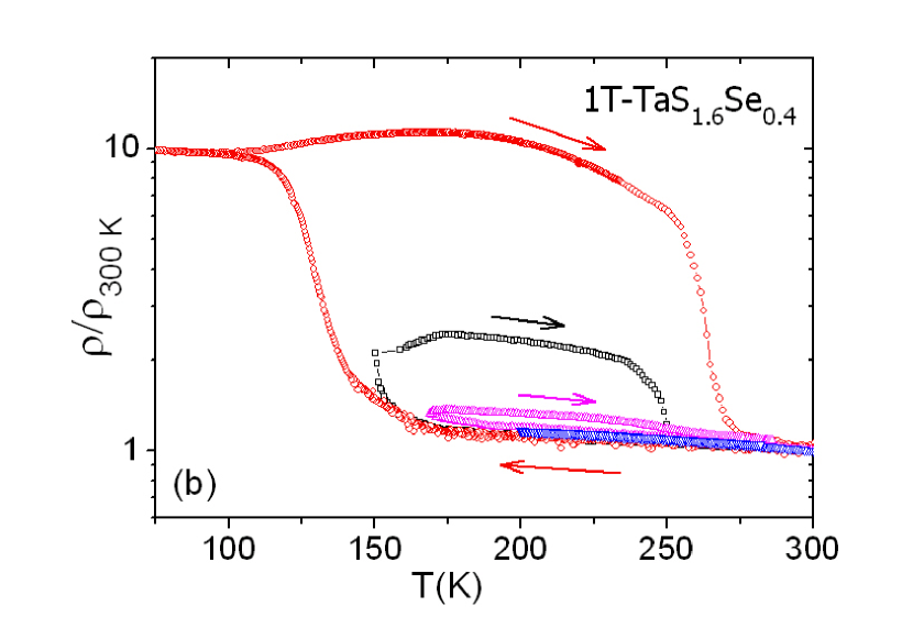
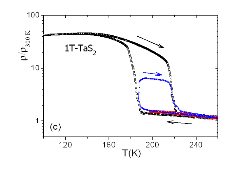
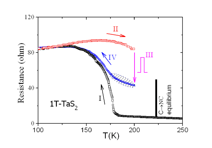
The temperature dependent resistivity (), and the hysteresis features of 1T-TaS2 and 1T-TaS1.6Se0.4 upon warming, are consistent with previous reports DiSalvo ; Vaskivskyi ; Yoshida2 , see Fig. 1(a). Compared with the pristine 1T-TaS2, 1T-TaS1.6Se0.4 exhibits a widened hysteresis temperature range. For the hysteresis behavior in (), it is clear that the thermal history plays essential roles: the emergence of the high-resistance CCDW is closely related to the hysteresis, as shown in Fig. 1(b) for a 1T-TaS1.6Se0.4 specimen. From the various cooling-heating sweeps of (), the hysteresis becomes more remarkable as the phase transition goes deeper towards the CCDW state. Specifically, if cooling does not reach the critical temperature of the CCDW phase transition, no identifiable hysteretic feature can be observed. In other words, the CCDW phase is a prerequisite for the birth of the hysteresis. In the following, the experimental data were obtained at fixed temperatures in the hysteresis region after warming the cryostat from a deep CCDW state at T=30 K. Fig. 2(a) clearly shows the current voltage characteristic (CVC) of a typical 1T-TaS2 sample: the Joule heating induced characteristics (by continuously voltage sweeping) appear above 20 mA at T=160 K, 130 K and 100 K, whereas the primary state is recovered once the current goes towards zero. However, at T=200 K in the hysteresis region, a remarkable non-volatile behavior emerges as shown in Fig. 2(b).
Initially, the system is in the thermodynamically stable CCDW state with R= 60 ohm. Upon increasing current I, HR state is almost independent of current until a kink appears at a threshold = 10.0 mA. Further increase in current decreases the voltage up to slightly exceeding 20.0 mA in the CVC curves. On reducing current, an enhancement of the slope of the CVC emerges and persists down to I = 0 mA, exhibiting a nonvolatile resistance. In contrast to the forward current scan, the kink feature in the CVC does not appear in the backward scan, implying the LR state survives.
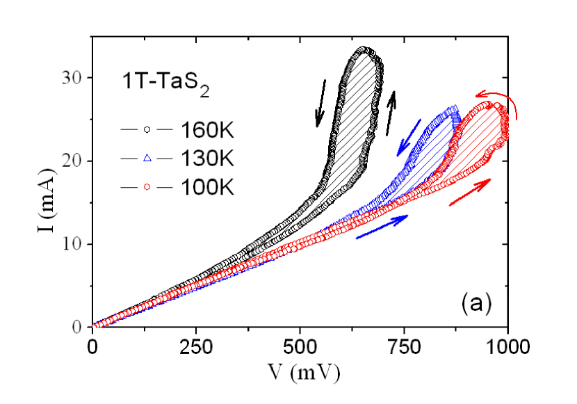
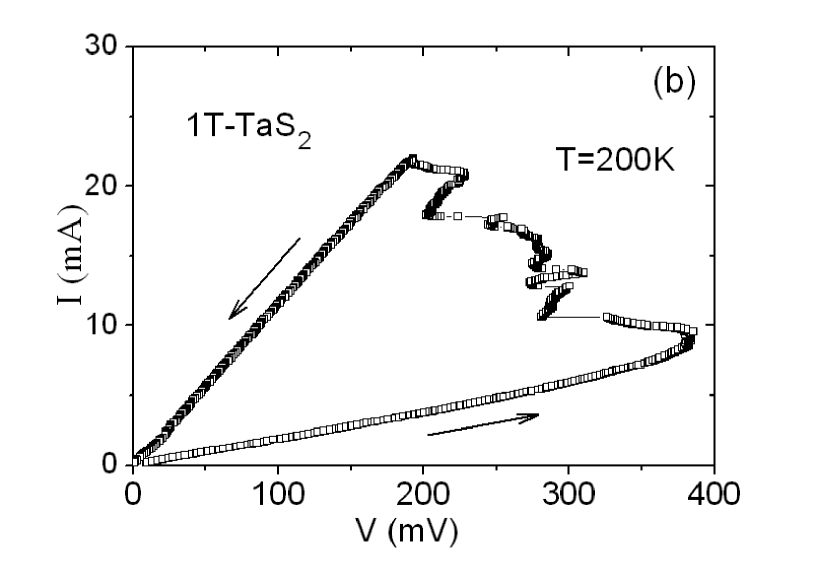
The resistance near I= 0 mA upon increasing current is distinctly different from the case of the inverse sweeping shown in Fig. 2(b), excluding the classical impurity pinning effects. We propose that this does not originate from the destruction of the sample, as the subsequent measurements with several thermal and electric field sweepings reproduced the data within experimental errors. The resistance-change effects are not associated with dielectric breakdown into filamentary paths, as in the memristor of a TaOx-based asymmetric passive device Huang ; Prakash . Zener tunnelling and avalanche breakdown can also be eliminated, for the occurrence of metastability in our experiments. The experimental results definitely showed that the sample states are intimately related to the history of the measurement, similar to the original nonvolatile switching results reported by Yoshida et al. Yoshida ; Yoshida2 and Tsen et al. Tsen . In comparison, the threshold electric field in our experiments is remarkably smaller than the results of Hollander et al. Hollander , probably due to higher temperature of the specimen and the finite-size effects McCarten for the CDW systems.
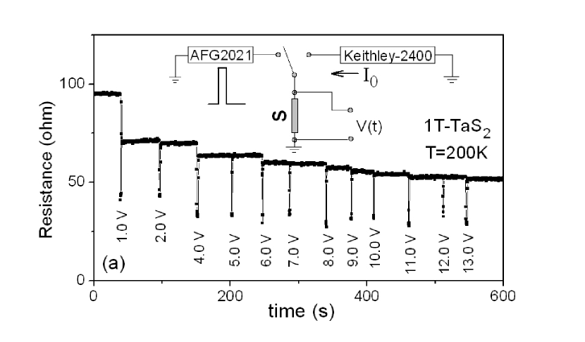
The transitions from one meta-stable state to another by current sweeping indicate that the applied electric field may have important effects on the 1T-TaS2 system. To reveal the evolution of the transport properties with increasing dc current, we investigated the electric pulse response of 1T-TaS2 and 1T-TaS1.6Se0.4 samples systematically. To avoid the Joule heating, the duration of pulses should be shorter than the relaxation time of the sample by self-heating, , where is the number of moles of material with specific heat c and thermal conductance Cohen , L and S are the length and the cross-section area of the specimen, respectively. In our experiments, it is estimated that 80 s Yongchang_2019 , so we applied single pulse with duration 40 s, the undistorted wave form of the response indicates that the Joule-heating effects could be neglected.
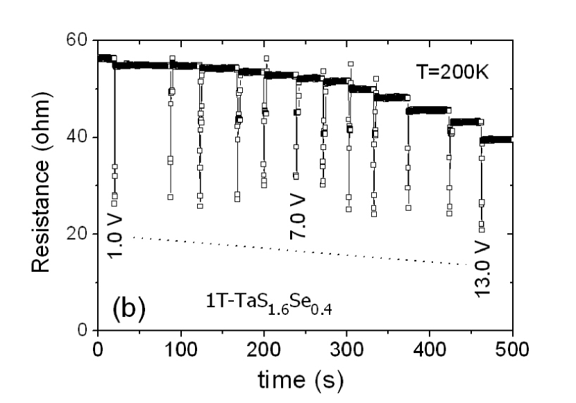
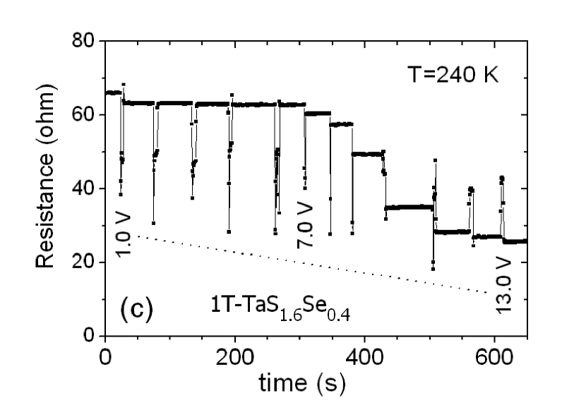
At T=200 K, a typical temperature in the hysteresis region, we conducted the measurement using the circuit schematically shown in the inset of Fig. 3(a). Similar results could also be seen in Figs. 3(b) and 3(c) for Se doped sample 1T-TaS1.6Se0.4. It is clear that the resistive changes at small voltages are more significant in the pristine crystal 1T-TaS2 than in 1T-TaS1.6Se0.4. The associated driving force may be from the larger ‵temperature gap′ from the measured temperature 200 K to the CNC CDW transition of 1T-TaS1.6Se0.4 (T=260 K) compared with 1T-TaS2 (T=220 K). The results in Figs. 3(b) and 3(c) (and also our results in Ref. Yongchang_2019 ) indicate that the closer to the CNC CDW transition the more significant of the resistance changes. After each electric pulse, an abrupt decrease of the resistance appears, and then maintains the state quickly without remarkable relaxation processes in our time resolution. It is obvious that pulses stimulate the configuration of the system to a new meta-stable state, and the series of pulses applied induce the multi steps of the resistance. It is believed that further applying higher electric pulses could drive the system to the states with larger conductivities, even the NCCDW phase. In other words, there are multi meta-stable states between CCDW and NCCDW phases, thus the energy differences between the meta-stable states would be very small Tsen . If it is the case, the thermal energy 200 K (17 meV) would smear out the distinctions between the multi meta-stable states, which is in conflict with the experimental data. In Ref. Yongchang_2019 , we have proposed a model to explain the multi meta-stable states or namely, nonvolatile resistance behavior, induced by electric pulses: each meta-stable state corresponds to a mixed state where the CCDW domains are separated by metallic regions, and the conductance of the whole system varies with the ratio of the two components.
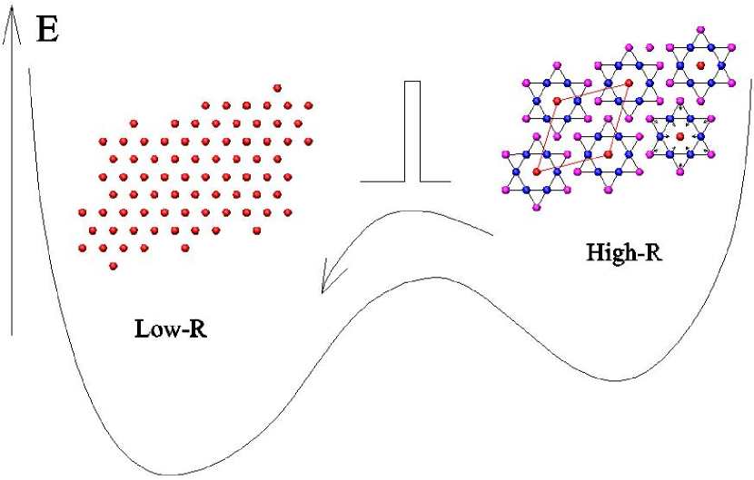
Thus we suggest the scenario for charge dynamics of 1T-TaS2 in the hysteresis region: in the absence of the electric pulse, the system is in a meta-stable CCDW state [see 4(a)], consisting of the David-star unit cells in which the electrons are bound inside, a state of HR. Within the electric pulse duration, the CCDW phase is excited to bear considerable strain or distortions, see Fig. 4(b). For a pulse with moderate magnitude, the excited state is not a full NC state as it would correspond to about 1/10 of the CCDW resistance, whereas in our experiments the resistance jump is no more than a half as shown in Figs. 3(a) and 3(b). With further increasing the magnitudes of the electric pulses at T=240 K for 1T-TaS1.6Se0.4 [in Fig. 3(c)], it appears that the resistance value comes closer to NCCDW state as shown schematically in Fig. 4(c). Considering the system can relax back to the equilibrium CCDW state after the activation of electric pulses below 130 K (see Supplementary Information I), whereas in hysteresis region the resistance value no longer restores the initial value (the intact CCDW state), we propose there should be some region with higher conductivities emerge in the CCDW environment and survive. In these high-conductance components, the David stars are expected to be unbounded/liberated by the electric pulses and the concentration of free carriers proliferates, forming ‵blank′ regions outside of CCDW domains and corresponding to the transition over the energy barrier in Fig. 5. This carrier proliferation process is not the same as formation of the domain walls in the hidden state in Refs. MaLG ; Karpov ; Cho , due to the higher temperature range in our present experiments and the relaxations after electric pulses (see Supplementary Information).
The validity of our proposal is supported by the results in Fig. 6. After applied electric pulses at T=200 K, the measured resistance shows an obvious enhancement with cooling, and below 150 K the system reverts back to the thermodynamically stable CCDW state, exhibiting a widened temperature range of the transition process. In other words, the starting point shifts towards higher temperature compared with the thermodynamically accessible NCC phase transition. The origin is likely the inhomogeneity of the CCDW domains induced by pulses [see Fig. 4(b)], and thus a spread phase transition accordingly. It is expected that the larger the domains, the higher transition temperature to the CCDW state, as the thermal disturbance becomes insignificant. In comparison, for the thermodynamically accessible NCC transition, as the NC phase consists of regular CCDW domains separated by discommensurabilities Thomson , the phase transition occurs homogeneously and sharply.
There are several possible explanations for the nonvolatile electric resistance behavior. The Frenkel-Kontorova (FK) model of the incommensurate commensurate transition for the emergence of Devil′s staircase Bak is related to the numerous minima of the free energy landscape, forming different meta-stable states of the system. In 1D-CDW, Gruner proposed that in a macroscopic specimen, the number of meta-stable states is about the ratio of its scale to the coherence lengths Gruner . Refs. MaLG ; Lee suggest that the inter-layer stacking is a decisive factor in determining the electronic structure of 1T-TaS2. In a very recent report Yoshida3 , Yoshida et al. proposed that in the transient unsteady state where the current is increased, the inter-layer coherence can be lost even inside a CDW domain. As some CDW layers move an atomically short distance ahead of the adjacent layers to settle into a meta-stable stacking configuration, the resistance changes are eventually established.
Though the whole mechanisms of the multi resistance states induced by electric pulses has not been completely disclosed yet, the potential applications are of interest in SSED. Recently, an asymmetric passive switching device was used in Pt/W/TaOx/Pt Kim ; Prakash . Besides the function of switches by applying appropriate voltages, the device with tunable multi-level resistance states induced by electric pulses could be used for synaptic devices in neuromorphic computing. We note that, in comparison, the creation and operating for case of 1T-TaS2 costs much less since it is only a two-terminal device, like a conventional resistor.
In summary, the electric pulses induced responses of 1T-TaS2 and 1T-TaS1.6Se0.4 crystals in the commensurate charge-density-wave phase in hysteresis temperature range have been investigated. The Joule heating effects were successfully avoided by the application of single electric pulse with duration of 40 s. Abrupt multi steps of the resistance excited by electric pulses were observed without remarkable relaxation processes above or at 200 K. Se doping widens the hysteresis region of 1T-TaS1.6Se0.4 crystal, and thus enhances the usage temperature of the nonvolatile resistance properties in the layered dichalcogenides. We propose that the response of the system may correspond to the rearrangements of the textures of CCDW domains, The multi-resistance states excited simply by electric pulses have profound significance for the explorations of solid-state devices.
Data Availability Statement — All the data that support the findings of this study are available from the corresponding author upon reasonable request.
Supplementary Material — See supplementary material for supportive data and the associated studies of the mixed state.
ACKNOWLEDGMENTS: The research work was supported by the National Science Foundation of China (Grant No. 10704054) and Tianjin Natural Science Foundation (No. 19JCYBJC30500). Work at Brookhaven National Laboratory is supported by the US DOE, Contract No. DE-SC0012704.
References
- (1) Masatoshi Imada, Atsushi Fujimori and Yoshinori Tokura, Rev. Mod. Phys. 70, 1039 (1998).
- (2) M. Yoshida, R. Suzuki, Y. J. Zhang, M. Nakano, and Y. Iwasa, Sci. Adv. 1, e1500606 (2015).
- (3) M. J. Hollander, Y. Liu, W. J. Lu, L. J. Li, Y. P. Sun, J. A. Robinson, and S. Datta, Nano Lett. 15, 1861 (2015).
- (4) I. Vaskivskyi, J. Gospodaric, S. Brazovskii, D. Svetin, P. Sutar, E. Goreshnik, I. A. Mihailovic, T. Mertelj, D. Mihailovic, Sci. Adv. 1, e1500168 (2015).
- (5) I. Vaskivskyi, I. A. Mihailovic, S Brazovskii, J. Gospodaric, T. Mertelj, D. Svetin, P. Sutar, and D. Mihailovic, Nat. Commun. 7, 11442 (2016).
- (6) W. Kim, A. Chattopadhyay, A. Siemon, E. Linn, R. Waser and V. Rana, Sci. Rep-UK 6, 36652 (2016).
- (7) X. Huang, K. Jiang, Y. Niu, R. Wang, D. Zheng, A. Dong, X. Dong, C. Mei, J. Lu, S. Liu, Z. Gan, N. Zhong and H. Wang, Appl. Phys. Lett. 113, 112103 (2018).
- (8) Amit Prakash, Debanjan Jana and Siddheswar Maikap, Nanoscale Research Lett. 8, 418 (2013).
- (9) Y. B. Nian, J. Strozier, N. J. Wu, X. Chen, and A. Ignatiev, Phys. Rev. Lett. 98, 146403 (2007).
- (10) M. J. Rozenberg, I. H. Inoue, and M. J. Snchez, Phys. Rev. Lett. 92, 178302 (2004).
- (11) L. Stojchevska, I. Vaskivskyi, T. Mertelj, P. Kusar, D. Svetin, S. Brazovskii, D. Mihailovic, Science 344, 177 (2014).
- (12) D. Wu, Y. C. Ma, Y. Y. Niu, Q. M. Liu, Tao Dong, S. J. Zhang, J. S. Niu, H. B. Zhou, Jian Wei, Y. X. Wang, Z. R. Zhao, and N. L. Wang, Sci. Adv. 4, eaao3057 (2018).
- (13) T. Ritschel, J. Trinckauf, K. Koepernik, B. Buchner, M. V. Zimmermann, H. Berger, Y. I. Joe, P. Abbamonte, and J. Geck, Nat. Phys. 11, 328 (2015). T. Ritschel, H. Berger, and J. Geck, Phys. Rev. B 98, 195134 (2018).
- (14) R. E. Thomson, B. Burk, A. Zettl, John Clarke, Phys. Rev. B. 49, 16899 (1994).
- (15) Y. Ma, Z. Wang, Y. Hou, D. Wu, C. Lu, and C. Petrovic, Phys. Rev. B 99, 045102 (2019).
- (16) F. J. Di Salvo, J. A. Wilson, B. G. Bagley, and J. V. Waszczak, Phys. Rev. B 12, 2220 (1975).
- (17) J. A. Wilson, F. J. Di Salvo, and S. Mahajan, Adv. Phys. 24, 117 (1975).
- (18) B. Dardel, M. Grioni, D. Malterre, P. Weibel, Y. Baer, and F. Levy, Phys. Rev. B 46, 7407 (1992).
- (19) L. V. Gasparov, K. G. Brown, A. C. Wint, D. B. Tanner, H. Berger, G. Margaritondo, R. Gal, and L. Forr, Phys. Rev. B. 66, 094301 (2002).
- (20) A. W. Tsen, R. Hovden, D. Z. Wang, Y. D. Kim, J. Okamoto, K. A. Spoth, Y. Liu, W. J. Lu, Y. P. Sun, J. Hone, L. F. Kourkoutis, P. Kim, and A. N. Pasupathy, Proc. Natl Acad. Sci. USA 112, 15054 (2015).
- (21) B. Sipos, A. F. Kusmartseva, A. Akrap, H. Berger, L. Forro and E. Tuti Nature Materials 7, 960 (2008).
- (22) Y. Yu, F. Yang, X. F. Lu, Y. J. Yan, Y. Cho, L. Ma, X. Niu, S. Kim, Y. Son, D. Feng, S. Li, S. Cheong, X. H. Chen and Y. Zhang, Nat. Nanotechnol. 10, 270 (2015).
- (23) K. Ludwiczak, E. Lacinska, J. Binder, I. Lutsyk, M. Rogala, P. Dabrowski, Z. Klusek, R. Stepniewski, A. Wysmolek, Solid State Comm. 305, 113749 (2020).
- (24) T. Endo, W. Yamaguchi, O. Shiino, T. Hasegawa, and K. Kitazawa, Surface Science 453, 1 (2000).
- (25) Yongchang Ma, Yanhui Hou, Cuimin Lu, Lijun Li and Cedomir Petrovic, Phys. Rev. B 97, 195117 (2018).
- (26) M. Yoshida, T. Gokuden, R. Suzuki, M. Nakano, and Y. Iwasa, Phys. Rev. B 95, 121405(R) (2017).
- (27) J. McCarten, D. A. DiCarlo, M. P. Maher, T. L. Adelman, and R. E. Thorne, Phys. Rev. B 46, 4456 (1992).
- (28) Marshall J. Cohen and A. J. Heeger, Phys. Rev. B 16, 688 (1977).
- (29) L. Ma, C. Ye, Y. Yu, X. F. Lu, X. Niu, S. Kim, D. Feng, D. Tomanek, Y. Son, X. H. Chen and Y. Zhang, Nature Comm. 7, 10956 (2016).
- (30) Petr Karpov and Serguei Brazovskii, Scientific Reports 8, 4043 (2018).
- (31) Doohee Cho, Sangmo Cheon, Ki-Seok Kim, Sung-Hoon Lee, Yong-Heum Cho, Sang-Wook Cheong and Han Woong Yeom, Nature Comm. 7, 10453 (2016).
- (32) P. Bak, Rep. Prog. Phys. 45, 587 (1982).
- (33) G. Gruner, Rev. Mod. Phys. 60, 1129 (1988).
- (34) Masaro Yoshida, Takuro Sato, Fumitaka Kagawa and Yoshihiro Iwasa, Phys. Rev. B 100, 155125 (2019).
- (35) Sung-Hoon Lee, Jung Suk Goh, and Doohee Cho, Phys. Rev. Lett. 122, 106404 (2019).