Tuning flexoelectricty and electronic properties of zig-zag graphene nanoribbons by functionalization
Abstract
The flexoelectric and electronic properties of zig-zag graphene nanoribbons are explored under mechanical bending using state of the art first principles calculations. A linear dependence of the bending induced out of plane polarization on the applied strain gradient is found. The inferior flexoelectric properties of graphene nanoribbons can be improved by more than two orders of magnitude by hydrogen and fluorine functionalization (CH and CF nanoribbons). A large out of plane flexoelectric effect is predicted for CF nanoribbons. The origin of this enhancement lies in the electro-negativity difference between carbon and fluorine atoms, which breaks the out of plane charge symmetry even for a small strain gradient. The flexoelectric effect can be further improved by co-functionalization with hydrogen and fluorine (CHF Janus-type nanoribbon), where a spontaneous out of plane dipole moment is formed even for flat nanoribbons. We also find that bending can control the charge localization of valence band maxima and therefore enables the tuning of the hole effective masses and band gaps. These results present an important advance towards the understanding of flexoelectric and electronic properties of hydrogen and fluorine functionalized graphene nanoribbons, which can have important implications for flexible electronic applications.
I Introduction
The coupling between polarization and strain gradients is an electro-mechanical phenomenon, which can be observed by bending a material. This is known as flexoelectricity, which is present in a variety of materials including soft matter Deng et al. (2014); Porenta et al. (2011); Petrov et al. (1989), liquid crystals Meyer (1969); Takahashi et al. (1998) and crystalline materials Tagantsev (1986); Ma and Cross (2006); Lu et al. (2012); Narvaez et al. (2015); Stengel (2015). The redistribution of charges induces flexoelectricity in materials due to the appearance of strain gradients and it has two microscopic contributions — electronic and ionic. The presence of non-uniform strain in a dielectric solid redistributes the ionic charges, leading to the appearance of ionic polarization, whereas the electronic polarization originates from the arrangement of the electronic clouds in the material under applied strain. The dependence of the induced electric polarization upon mechanical deformation of a material is expressed as Yudin and Tagantsev (2013):
| (1) |
where Pi, , and are the components of the polarization, the strain tensor, the piezoelectric tensor and the flexoelectric tensor, respectively.
Following the discovery of flexoelectricity it was found to be a weak effect, which is hardly detectable in bulk materials. Since the induced polarization depends on both the strain gradient and the flexoelectric coefficient; a large gradient is required to generate considerable polarization. A lot of recent experimental efforts have focused on flexoelectricity in perovskite thin films of (Ba/Sr)TiO3 Cross (2006); Lu et al. (2012) where the strain gradient was introduced during the epitaxial growth Li et al. (2015); Ji et al. (2010); Lee et al. (2011). Additionally the recent discovery of strain gradient mediated photovoltaic response in BaFeO3 Chu et al. (2015) has renewed the interest in flexoelectricity.
Different from bulk materials, layered two-dimensional materials (2D) are able to sustain large strain gradients and are therefore expected to show strong flexoelectricity Duerloo and Reed (2013); Naumov et al. (2009); Michel et al. (2016); Kundalwal et al. (2017). For instance, graphene monolayer is one of the best known elastic materials and it can sustain more than 10 % mechanical strains Lee et al. (2008); zha (2020). Together with these superior elastic properties, the reduced lattice symmetry of 2D materials makes them promising for piezo- and flexoelectric applications Michel et al. (2016, 2017); Dong et al. (2017). For example monolayer MoS2 Dong et al. (2017); Wang et al. (2019) and its Janus structures Dong et al. (2017); Yagmurcukardes et al. (2019) exhibit large out of plane piezoelectricity exceeding the most common 3D piezoelectric crystal AlN Bechmann (1958). Experimentally, the electro-mechanical properties of monolayer MoS2 were explored by perturbing the structure by atomic force microscopy and a large flexoelectric effect induced by the structural deformation was proposed Abdollahi et al. (2019).
| System | (Å) | (Å) | (Å) | width (Å) | (Å) | (Å) | (Å) | (Å) | Cb (eVnm2) | Nchain | Fzyzy (nC/m) |
|---|---|---|---|---|---|---|---|---|---|---|---|
| C | 2.47 | 4.278 | 0 | 77.006 | 1.43 | 0.66 | 0.927 | 36 | 0.0004 | ||
| CH | 2.54 | 4.40 | 0.46 | 79.12 | 1.54 | 1.11 | 2.68 | 1.68 | 36 | 0.035 | |
| CF | 2.60 | 4.50 | 0.49 | 81.06 | 1.58 | 1.38 | 3.25 | 1.76 | 36 | 0.062 | |
| CHF | 2.58 | 4.47 | 0.47 | 80.44 | 1.56 | 1.11 | 1.39 | 2.96 | 1.43 | 36 | 0.167 |
Pure graphene, on the other hand, due to its centrosymmetric nature (point group D6h) does not exhibit any piezoelectric properties. Several studies have focused on improving electro-mechanical properties of graphene by breaking its perfect planar symmetry in graphitic membranes Kalinin and Meunier (2008), carbon nanocones Kvashnin et al. (2015), carbon nanoshells Dumitrică et al. (2002), nanotubes White and Mowrey (1993); Artyukhov et al. (2020), graphene nanoribbon springs Javvaji et al. (2020), moiré superlattices McGilly et al. (2020) and by introducing various type of defects in perfect graphene sheet Javvaji et al. (2018). However, in all the above mentioned studies the flexoelectricity is induced by symmetry breaking of orbitals under structural deformation which remains weak Kalinin and Meunier (2008); Kvashnin et al. (2015); Dumitrică et al. (2002); Javvaji et al. (2018). Besides mechanical strains Ferralis et al. (2008); Kim et al. (2009) and graphene origami Chen et al. (2019); Wei et al. (2020); Ma et al. (2020), atomic functionalization is another popular experimental technique for engineering novel functionalities in graphene Lee et al. (2012); Johns and Hersam (2013); Elias et al. (2009); Pumera and Wong (2013); Jørgensen et al. (2016); Wheeler et al. (2012). Previous reports have shown that the electronic properties of graphene can be modified by functionalization Paupitz et al. (2012); Jørgensen et al. (2016); Yan et al. (2012). Functionalization has also been used to induce piezoelectricity in graphene monolayer by adsorbing adatoms (such as H, F, Li) on a single side of the graphene monolayer Ong and Reed (2012), or by co-adsorption of H and F Ong et al. (2013); Kim et al. (2014).
Here, by performing state of the art first-principles calculations we propose that the rather inferior flexoelectric properties of graphene zig-zag nanoribbons (ZNRs) can be significantly improved in their hydrogen/fluorine functionalized variants in CH and CF nanoribbons. Due to the charge and ion redistribution upon bending, these ZNRs exhibits a net dipole moment which is linearly dependent on the applied strain gradient. We further show that the flexoelectric properties can be further improved in CHF type Janus ZNR by breaking both structural and charge symmetry. The bending energy of all ZNRs is small implying the feasibility of the proposed bending scheme. Furthermore, the electronic properties and hole effective masses can also be tuned by mechanical bending.
II Theoretical and computational details
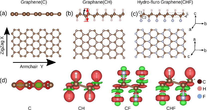
We start from zig-zag nanoribbons of graphene (C), graphane (CH), fluoro-graphene (CF) and hydro-fluoro-graphene (CHF). The lattice parameters for the corresponding monolayers and widths of the considered nanoribbons are listed in Table 1. The bent ZNR structures were created by displacing the positions of atoms with a quadratic function which depends on the position of atoms (). Here is the strain gradient of the bending plane defined as . All the curved structures were generated by an in-house developed python workflow utilizing the Atomsk library Hirel (2015). For all ZNRs the bending is applied along direction. Additional details regarding the bending model employed here can be found in Refs. Javvaji et al. (2020); Zhuang et al. (2019); Hu et al. (2019).
These geometries were subsequently relaxed within density functional theory (DFT) simulations. All DFT calculations were performed within the Vienna Ab initio Simulation Package (VASP) Kresse and Furthmüller (1996) by using the projector augmented wave method with the Perdew-Burke-Ernzerhof (PBE) exchange correlation functional Blöchl (1994); Kresse and Joubert (1999); Perdew et al. (1996). Periodic boundary conditions were applied in the direction to simulate the curvature of an infinitely long ribbon. A vacuum region of 25 Å was used along and directions. The edges of all ZNRs studied here were passivated with hydrogen. For the curved ribbons the edge atoms were kept fixed along and direction during structure relaxation while all interior atoms were fully relaxed by using a conjugate-gradient scheme until the force on the atoms were less than 0.01 eV/Å. For flat ZNRs all atoms were relaxed. A 15 1 1 k-point grid was used to sample the Brillouin zone and energy convergence criteria of 110-5 was used during the structure relaxation. These calculations parameters and convergence criteria are standard and similar to those used in previous studies on mechanical properties of graphene and other related 2D materials Yu et al. (2016); Nepal et al. (2019).
As discussed in the previous studies Zhuang et al. (2019); Hu et al. (2019) the applied bending perturbation only induces the strain component and the strain gradient term (), whereas the remaining components of the strain and strain gradient tensors are zero Zhuang et al. (2019); Hu et al. (2019). Therefore, the total induced polarization () given by Eq. (1) can be rewritten along the -direction as:
| (2) |
The dipole moment along the direction () was calculated with respect to the center of mass of the unit cell for all the systems. For dipole moment calculation a dense k-grid (51 1 1) along with a high energy cutoff of 550 eV were used. Subsequently, the vertical polarization of the curved structure was estimated by = , where is the effective volume of the flat ZNRs. Although the exact value of thickness () for monoatomic layers such as graphene is debatable Wang et al. (2005); Huang et al. (2006); Kalinin and Meunier (2008), here we assume a thickness of 0.66 Å (the spatial extent of the graphene orbitals) for graphene ZNRs. For functionalized ZNRs thickness is defined as the distance between outer most atoms as described in the Figure 1 (b). The effective thickness employed in this work for all nanoribbons is listed in the Table 1. This effective thickness was used in calculations of effective volume of nanoribbons for describing the induced polarization.
III Results and discussions
III.1 Bending stiffness
The relaxed structural parameters of C, CH, CF and CHF 2D layers corresponding to a rectangular unitcell are listed in Table 1. The most energetically favorable configuration for H and F co-adsorbed graphene monolayer (CHF structure in this work) was previously explored by Reed et. al. Ong et al. (2013); Ong and Reed (2012). They showed that the structure with hydrogen and fluorine being adsorbed on alternating atop carbon sites (the so called chair configuration) is energetically most favorable. We use this configure for creating the CHF structure. The various structural parameters are highlighted in Figure 1(a-c). Among these monolayers, graphene has the smallest and CF has the largest lattice parameter. Due to its higher electro-negativity, F induces larger buckling (0.49 Å) than hydrogen (0.46 Å). The induced charge distribution of all these monolayers is shown in Figure 1(d). Even with complete hydrogenation or fluorination the centrosymmetry of the system is preserved and the charge distribution is symmetric. However, due to large electro-negativity difference H and F co-adsorption on graphene monolayer (CHF monolayer) breaks the symmetry, which results in a net dipole moment of 0.48 eÅ. Furthermore, the Janus CHF monolayer has asymmetric bond lengths and bond angles. As explained later this will have important consequences on out-of-plane flexoelectricty. These monolayers are repeated along the direction to create ZNRs with a finite width along the -direction. The width of all the ZNRs studied here is listed in Table 1.
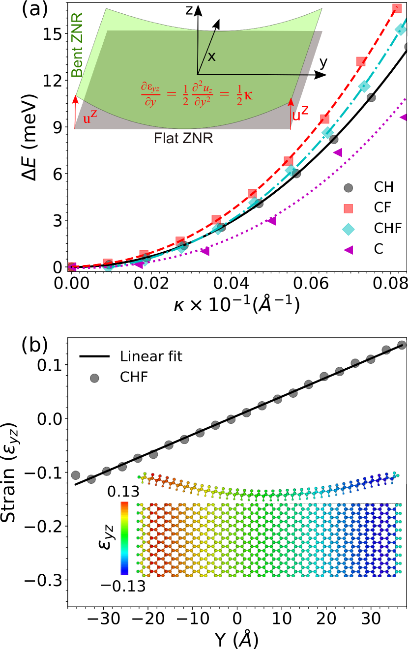
Next, we calculate the bending energy and bending stiffness of C, CH, CF and CHF ZNRs subjected to the bending perturbation described above. Within the strain gradient range explored here the bending energy of all ZNRs is smaller than 18.32 meV/Å2 — the van der Waals binding energy of bulk graphite Lebègue et al. (2010); Yu et al. (2016). This small energy implies that the bending scheme employed in this work can be readily achieved via mechanical bending or can be introduced during growth. The bending stiffness () is calculated by taking the second derivative of the strain energy on a per atom basis (energy difference between the flat and the bent ZNRs divided by the number of atoms) with respect to the strain gradient () as shown in Figure 2(a). The lowest bending stiffness of 0.927 eVnm2 is obtained for C ZNRs, followed by CH, CHF and CF ZNRs. Note that the bending stiffness values obtained here are higher than the previously reported values Mintmire and White (1995); Kudin et al. (2001); González et al. (2018) for graphene, where the bending scheme was related to the generation of carbon nanotubes. However, the bending scheme employed in this work displaces the atoms only along the direction resulting in higher perturbation of bond lengths and therefore a larger bending stiffness is obtained.
III.2 Bending induced strain and flexoelectricity
As alluded before the bending model employed here induces a strain in direction and a strain gradient in the direction and that in-turn gives rise to induced polarization along the direction. Figure 2(b) shows the linear dependence of with respect to atomic positions for CHF ZNRs at 0.0073 Å-1 strain gradient. The inset of Figure 2(b) presents the strain component projected onto CHF atomic structure. The atomic strain at site is computed according to Li and Shimizu (2005); Shimizu et al. (2007); Stukowski (2009)
| (3) |
where is the deformation strain gradient tensor and I is the identity matrix. As reported previously Zhuang et al. (2019); Javvaji et al. (2019) the strain induced in the directions varies linearly, indicating the symmetric nature of induced deformation. Therefore, any contribution to the induced polarization due to in Eq. 2 is eliminated.
Accordingly, the flexoelectric response () is described as the induced polarization due to a strain gradient, which in this case can be described as Zhuang et al. (2019); Hu et al. (2019); Javvaji et al. (2019):
| (4) |
From the slope of Figure 2(b) we can obtain (), which includes the effect of structural relaxation on the applied strain gradient. For instance, the slope of Figure 2(b) gives as 0.0035 Å-1, which is 3.5% smaller than the actual applied . Similarly, we find that for all the systems studied here is 2-5% smaller than the initial applied . This is subsequently used in the calculation of the flexoelectric coefficients.
III.2.1 Flexoelectricity in C, CH and CF zig-zag nanoribbons
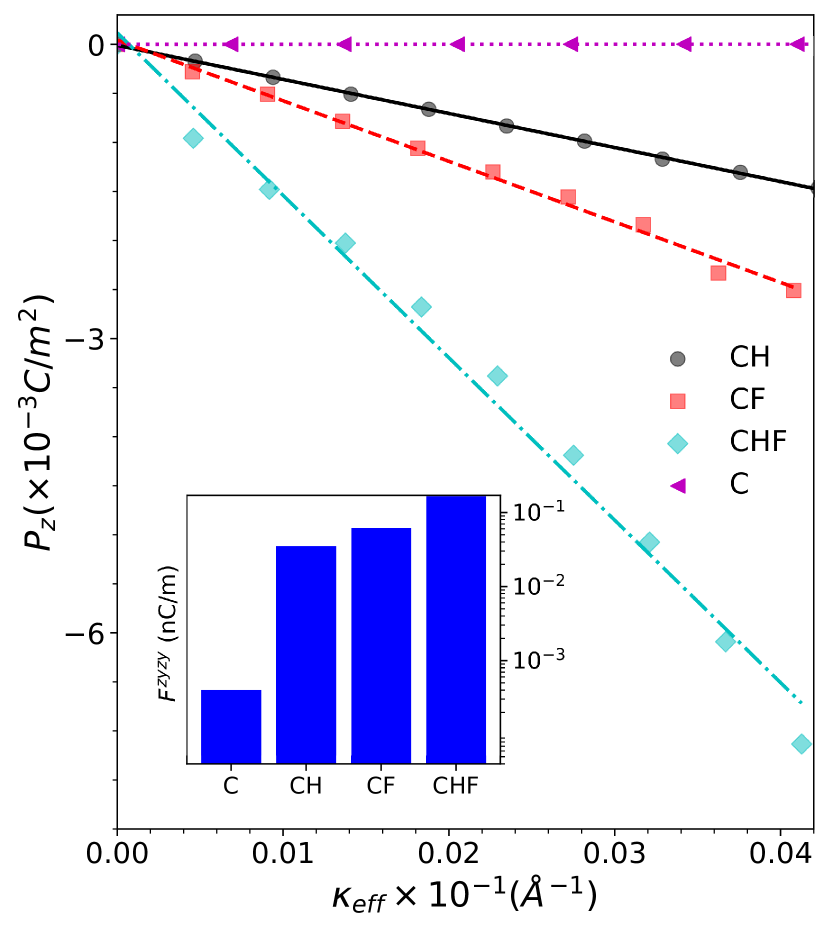
The estimated induced polarization (dipole moment per unit volume) is plotted in Figure 3 as a function of . As expected, with increasing , due to higher non-linear strain gradients, the magnitude of induced polarization also increases. The out of plane flexoelectric coefficient can then be obtained by linearly fitting the induced polarization, which is plotted in the inset of Figure 3. The lowest flexoelectric coefficient was observed for graphene ZNRs, followed by CH and CF ZNRs, respectively. For graphene ZNRs the calculated flexoelectric coefficient is 0.0004 nc/m. Initially, for the flat graphene ZNR the out of plane dipole moment is zero, however as the graphene ZNR is bent the - interactions begin to increase, which induces a net non zero dipole moment along direction. To analyse the effect of strain gradient on the induced polarization, the electronic and ionic components of the dipole moment were calculated within the Berry phase method Spaldin (2012); Vogl (1978); Resta (1994). We find that for graphene nanaribbons with increasing the ionic component of the dipole moment exhibits a larger change than the electronic part of the dipole moments. Moreover, as the increases, the contribution from the electronic component becomes much more important. For example, for a strain gradient of 0.002 Å-1, while 93.4 % of the total dipole moment has an ionic origin, only 5.6 % has an electronic one. When the increases to 0.004 Å-1 the contribution of ionic and electronic component of the dipole moments becomes 91.1 % and 7.9 %, respectively. The increase in electronic dipole moment with bending can be attributed to the enhanced - interactions originating from strain gradient driven to hybridization transition Dumitrică et al. (2002); Kundalwal et al. (2017). This is also in agreement with a recent study on graphene where the polarization was calculated from a charge-dipole model Zhuang et al. (2019); Kundalwal et al. (2017).
As shown in Figure 3 the induced polarization for CH and CF ZNRs is much larger than that in graphene ZNRs. The higher induced polarization results in larger values of 0.035 nC/m and 0.062 nC/m for CH and CF ZNRs, respectively. Structurally there are two main differences between C and CH/CF ZNRs; (i) H or F atoms induce buckling (0.46-0.49 Å) in the flat graphene sheet and (ii) the out of plane CH bonds provide additional avenues for tuning the charge transfer under mechanical bending. As previously noted for buckled silicene Zhuang et al. (2019) such structural buckling is useful for generating higher flexoelectricity.
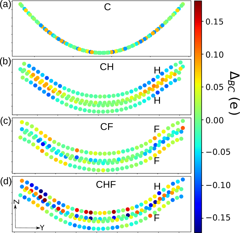
To investigate the effect of H/F atoms on flexoelectric properties we next analyse the Bader charges Sanville et al. (2007); Tang et al. (2009). Initially, for the flat ( = 0) CH and CF ZNRs, the Bader charges of both top and bottom H (0.11e) and F (0.52e) are equal. As the bond lengths between top and bottom H (F) and C atoms are the same, the dipole moment of C-Hbottom (C-Fbottom) bond cancels the dipole moment of other C-Htop (C-Ftop) bond, resulting in a net zero total dipole moment. The charge symmetry of these top and bottom C-H or C-F bonds is perturbed under applied strain gradient. The changes in Bader charges with respect to flat ZNRs at of 0.0041Å-1 are shown in Figure 4.
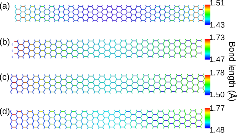
As can be seen, the bending modifies the bond lengths (shown in Figure 5), therefore resulting in charge redistribution within the ZNRs. The magnitude of this charge redistribution is directly proportional to . For example, in graphene ZNRs (Figure 4) at = 0.0041 Å-1, the charge redistribution varies between 0.075e and 0.075e, resulting in a finite induced dipole moment. When bending is applied to the CH or CF ZNRs, along with C-C bond lengths, the out of plane C-H and C-F bond lengths also change. The C-C bond lengths at = 0.0041 Å-1 are shown in Figure 5(a-d). The larger bond length perturbation results in a larger redistribution of charges under bending. For instance, at the same (0.0041 Å-1) for CF monolayer the change in the Bader charges varies from 0.15e to 0.15e, which is much larger than in the graphene ZNR. Therefore, for similar , higher induced polarization is observed in CH and CF ZNRs, implying larger out of plane flexoelectric coefficients.
III.2.2 Flexoelectricity in CHF zig-zag nanoribbons
We next explore the possibility to enhance the flexoelectric properties of graphene ZNRs by dual functionalization i.e. creating CHF type ZNRs as shown in Figure 1(c). Due to the large electro-negativity difference between H (2.2) and F (3.98); the CH and CF bond lengths in a CHF monolayer are very different (Table 1). The charge density difference in a CHF monolayer is shown in Figure 1(d). As can be seen from Figure 1(d) for CHF monolayer the charge symmetry of C-H and C-F bonds is broken. The Bader charge analysis shows that both H (0.11e) and F (0.54e) atoms in the flat CHF ZNRs are negatively charged. Whereas, the averaged Bader charge on the C atoms connected to H is 0.11e and for those connected to F is 0.54e. Therefore, the local dipole induced in C-F bonds dominants over the C-H bonds, resulting in a net dipole moment. When the CHF ZNR is bent, the charge asymmetry in the buckled carbon layer is further increased. Due to the large electro-negativity difference between F and H atoms, the C1 atom (the carbon atom attached to H, as marked in 1(c)) and C2 atoms (carbon atom bonded to F) experience different perturbation, resulting in different charges on these atoms. When the ZNR is bend ( = 0.0041 Å-1) the charge in the CHF ZNR at the C1 site is enhanced by 20%, while the charge at the C2 site decrease by 12%. The corresponding number for CF ZNRs at C1 and C2 sites are 5% and 3%, respectively at the same . Therefore, for the same CHF ZNRs have higher induced polarization, implying an even larger flexoelectric coefficient. From the linear fitting of induced polarization our calculations predict a Fzyzy of 0.167 nC/m, which is nearly 2.5 times larger than the Fzyzy value for CF.
For CH and CF ZNRs due to the identical C-H or C-F bond lengths at the flat state the bending along direction is equivalent. However in the case of CHF ZNRs, C-F bond lengths are larger than C-H bond lengths, therefore bending along or direction may be energetically different. To investigate this further we compare the bending energy of CHF ZNRs along (bending is applied towards H atoms) and direction (bending is applied towards F atoms). We find that, bending along the direction (along C-H bonds) is energetically favorable and the energy difference relative to direction is 510 meV per unit cell (3.53 meV per atom basis) at = 0.0041 Å-1. Nonetheless, we computed the induced polarization of CHF ZNRs under bending along direction and find a Fzyzy of 0.154 nC/m. This value is comparable to the 0.167 nC/m, which is obtained for bending along direction.
Furthermore, to investigate the effect of the width of ZNRs on flexoelectric properties, additional calculations were performed for larger width CH and CHF ZNRs (w = 182.374 Å for CH and w = 184.87 Å for CHF). For these larger width CH and CHF ZNRs the calculated Fzyzy are 0.038 nC/m and 0.175 nC/m, respectively. These Fzyzy values are comparable (within 8 %, and 5 % for CH and CHF respectively) to the values computed with the smaller widths ZNRs listed in Table 1. Therefore, the width of ZNRs simulated here is likely large enough to eliminate finite size effects on the flexoelectric properties.
III.3 Effect of bending on the electronic properties
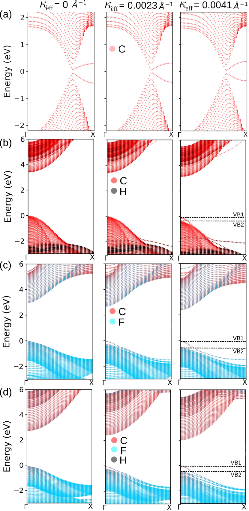
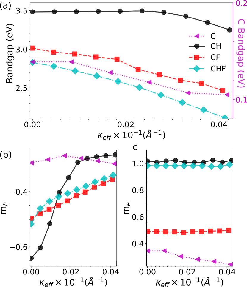
Mechanical bending also impacts the electronic properties as it can induce localization/delocalization in the electronic charges and modify hybridization. This change in the charge distribution leads to modifications of electronic properties such as the effective mass and band gap. The effect of bending on C, CH, CF and CHF ZNRs band structures is shown in Figure 6(a-d), respectively at selected values. Here atomic projected eigenvalue values are also shown in different colors. The variation of band gap as a function of is shown in Figure 7(a). Bending has no significant effect on the electronic properties of graphene ZNRs and with bending the band gap reduces by 0.032 eV as shown in Figure 7(a). The electronic structure of graphene is mainly sensitive to uni-axial in plane strain, twisting Tang et al. (2012) The bending scheme employed here induces a small in-plane strain, which is insufficient to induce any noticeable hybridization changes. This can also be co-related with the strain gradient induced polarization which is small in the case of C ZNRs. The effect of a strain gradient on C ZNRs hole () and electron effective masses is shown in Figure 7(b) and (c) and both and mostly remain unchanged.
The situation is different for CH, CF and CHF ZNRs, where electronic properties are sensitive to C-H, or C-F out of plane bonds as well. For the flat CH ZNRs the band gap is about 3.47 eV, where both VBM and CBM originate mainly from carbon atoms as shown in Figure 6(b). As the CH ZNR is bent, initially the band gap starts to decrease at a slower rate and as the bending exceeds 0.0025 Å-1 the band gap decreases sharply as shown in Figure 7(a). Overall, within the range explore here the band gap of CH ZNRs is reduced by 0.3 eV. In the case of CF and CHF ZNRs the band gap drops at a much faster rate as a function of bending. This is because for CH ZNRs the valence band maxima, originates from C atoms, however for CF and CHF ZNRs the VBM shows a strong hybridization between C and F atoms. When mechanical bending is applied, the distance between C-F atoms increases, which reduces the hybridization between C-F states, leading to large splitting between the VB1 and VB2 states as shown in Figure 6(b) and (c). The bending not only reduces the band gap of CH, CF and CHF ZNRs but also reduces the hole effective masses as shown in Figure 7(b), whereas the electron effective mass remains mostly unchanged (Figure 7(c)).
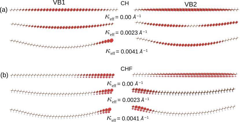
The variation of valence band partial charge density at VB1 and VB2 at -point (marked in Figure 7) is shown in Figure 8(a)-(b) for CH and CHF, respectively. Using mechanical bending as an external perturbation the distribution of these charges can be tuned together with the electronic properties Yu et al. (2016); Nepal et al. (2019). In the case of CH ZNRs at zero the charge carriers in both VB1 and VB2 states are delocalized over the entire ribbon width. With the increase in the charges of VB1 bands are localized towards the right edge of the ZNR. At the same time the charge density more or less remains distributed over the entire ribbon width for VB2. A different trend is observed for CF and CHF ZNRs. As shown in Figure 8(b), even at zero the partial charges in the CHF ZNRs are delocalized along the right edge and with increasing this edge charge delocalization becomes more prominent. Also, the charge in the VB2 state are more delocalized along the left edge. The large variation in the hole effective masses under for CH ZNRs can be explained on the basis of this partial charge density. When charges are distributed over the entire ribbons width the hole effective masses are larger. With increasing the charges get accumulated towards right edge the effective mass decreases. At higher , for VB1, all three ZNRs exhibit similar partial charge density and therefore the hole effective masses are comparable.
The dependence of bandgap on the ZNR width and number of zigzag chains is also studied. This is shown in the supplementary material Figure S1, along with the band structures of corresponding monolayers (Figure S2). As can be seen with the increasing width, the bandgap of all ZNRs decreases and converges to the bandgap value of corresponding monolayers. For graphene ZNRs our results are in good agreement with previous calculations of Son et. al. Son et al. (2006).
IV Discussion and Summary
Our extensive first-principles calculations unveil a significant out of plane flexoelectricity in functionalized graphene ZNRs which is comparable to the recently reported values for monolayer transition metal dichalcogenides Javvaji et al. (2019); Zhuang et al. (2019). We predict that flexoelectricity in hydro-fluorinated graphene ZNRs (CHF) is three times larger than that of CF ZNRs. This large enhancement in flexoelectricity is mainly facilitate by the large electro-negativity difference between H and F which breaks the structural and charge symmetry. By analyzing the electronic structure as a function of we find that for the functionalized ZNRs the hole effective mass can be reduced by 10%, whereas the electron effective mass mostly remains unchanged.
Previous reports have shown that single side H or F functionalization can induced strong piezoelectricty in graphene Paupitz et al. (2012); Jørgensen et al. (2016); Yan et al. (2012) and silicene Noor-A-Alam et al. (2015) monolayers. These could naturally also be an interesting avenue for tuning the flexoelectric properties. Our calculations for single side H functionalized graphene ZNR, predict a Fzyzy value of 0.053 nC/m which is higher than the value (0.035 nC/m) obtained for double side functionalized graphene (CH) ZNR. Although, we do not explicitly calculate properties for single side F functionalized C ZNRs, based on the trend observed for H functionalized ZNRs, relatively higher flexoelectric properties can be anticipated. Similarly, oxygen functionalized graphene ZNRs are also expected to show good flexoelectric properties. Moreover the ever growing interest in Janus 2D materials where intrinsically a local dipole moment is present due to symmetry breaking could provide an exciting platform for low dimensional flexoelectricity.
The main highlight of the above results is that the flexoelectric properties of many low dimensional materials could be significantly improved by simple functionalization, which is readily achievable in experiments. Additionally, the bending scheme proposed here could be realized via mechanical bending, or can be introduced during the growth. These results open new opportunities to take advantage of the unique mechanical bending of low dimensional materials not only to investigate their flexoelectric properties, but also to tune their physical properties such as band gap and effective masses. With the recent experimental advances in the growth of graphene nanoribbons Kolmer et al. (2020), we believe that our findings will stimulate future experimental exploration of flexoelectric properties of these and other similar compounds.
Acknowledgment
The computational resources and services used for the first-principles calculations in this work were provided by the VSC (Flemish Supercomputer Center), funded by the Flemish Science Foundation (FWO-VI). T. P. is supported by a postdoctoral research fellowship from BOF-UAntwerpen.
References
- Deng et al. (2014) Q. Deng, L. Liu, and P. Sharma, J. Mech. Phys. Solids 62, 209 (2014).
- Porenta et al. (2011) T. Porenta, M. Ravnik, and S. Zumer, Soft Matter 7, 132 (2011).
- Petrov et al. (1989) A. Petrov, R. Ramsey, and P. Usherwood, Eur. Biophys. J. 17, 13 (1989).
- Meyer (1969) R. B. Meyer, Phys. Rev. Lett. 22, 918 (1969).
- Takahashi et al. (1998) T. Takahashi, S. Hashidate, H. Nishijou, M. Usui, M. Kimura, and T. Akahane, Jpn. J. Appl. Phys. 37, 1865 (1998).
- Tagantsev (1986) A. Tagantsev, Phys. Rev. B 34, 5883 (1986).
- Ma and Cross (2006) W. Ma and L. E. Cross, Appl. Phys. Lett. 88, 232902 (2006).
- Lu et al. (2012) H. Lu, C.-W. Bark, D. E. De Los Ojos, J. Alcala, C.-B. Eom, G. Catalan, and A. Gruverman, Science 336, 59 (2012).
- Narvaez et al. (2015) J. Narvaez, S. Saremi, J. Hong, M. Stengel, and G. Catalan, Phys. Rev. Lett. 115, 037601 (2015).
- Stengel (2015) M. Stengel, Phys. Rev. B 92, 205115 (2015).
- Yudin and Tagantsev (2013) P. Yudin and A. Tagantsev, Nanotechnology 24, 432001 (2013).
- Cross (2006) L. E. Cross, J. Mater. Sci. 41, 53 (2006).
- Li et al. (2015) Y. Li, C. Adamo, P. Chen, P. G. Evans, S. M. Nakhmanson, W. Parker, C. E. Rowland, R. D. Schaller, D. G. Schlom, D. A. Walko, et al., Sci. Rep. 5, 16650 (2015).
- Ji et al. (2010) W. Ji, K. Yao, and Y. C. Liang, Adv. Mater. 22, 1763 (2010).
- Lee et al. (2011) D. Lee, A. Yoon, S. Jang, J.-G. Yoon, J.-S. Chung, M. Kim, J. Scott, and T. Noh, Phys. Rev. Lett. 107, 057602 (2011).
- Chu et al. (2015) K. Chu, B.-K. Jang, J. H. Sung, Y. A. Shin, E.-S. Lee, K. Song, J. H. Lee, C.-S. Woo, S. J. Kim, S.-Y. Choi, et al., Nat. Nanotechnol. 10, 972 (2015).
- Duerloo and Reed (2013) K.-A. N. Duerloo and E. J. Reed, Nano Lett. 13, 1681 (2013).
- Naumov et al. (2009) I. Naumov, A. M. Bratkovsky, and V. Ranjan, Phys. Rev. Lett. 102, 217601 (2009).
- Michel et al. (2016) K. H. Michel, M. Neek-Amal, and F. M. Peeters, Phys. Status Solidi B 253, 2311 (2016).
- Kundalwal et al. (2017) S. Kundalwal, S. Meguid, and G. Weng, Carbon 117, 462 (2017).
- Lee et al. (2008) C. Lee, X. Wei, J. W. Kysar, and J. Hone, Science 321, 385 (2008).
- zha (2020) Carbon 168, 135 (2020).
- Michel et al. (2017) K. Michel, D. Çakır, C. Sevik, and F. Peeters, Phys. Rev. B 95, 125415 (2017).
- Dong et al. (2017) L. Dong, J. Lou, and V. B. Shenoy, ACS Nano 11, 8242 (2017).
- Wang et al. (2019) X. Wang, A. Cui, F. Chen, L. Xu, Z. Hu, K. Jiang, L. Shang, and J. Chu, Small 15, 1903106 (2019).
- Yagmurcukardes et al. (2019) M. Yagmurcukardes, C. Sevik, and F. Peeters, Phys. Rev. B 100, 045415 (2019).
- Bechmann (1958) R. Bechmann, Phys. Rev. 110, 1060 (1958).
- Abdollahi et al. (2019) A. Abdollahi, N. Domingo, I. Arias, and G. Catalan, Nat. Commun. 10, 1 (2019).
- Kalinin and Meunier (2008) S. V. Kalinin and V. Meunier, Phys. Rev. B 77, 033403 (2008).
- Kvashnin et al. (2015) A. G. Kvashnin, P. B. Sorokin, and B. I. Yakobson, J. Phys. Chem. Lett. 6, 2740 (2015).
- Dumitrică et al. (2002) T. Dumitrică, C. M. Landis, and B. I. Yakobson, Chem. Phys. Lett. 360, 182 (2002).
- White and Mowrey (1993) C. White and J. M. R. Mowrey, Buckminsterfullerenes , 125 (1993).
- Artyukhov et al. (2020) V. I. Artyukhov, S. Gupta, A. Kutana, and B. I. Yakobson, Nano Lett. 20, 3240 (2020).
- Javvaji et al. (2020) B. Javvaji, B. Mortazavi, T. Rabczuk, and X. Zhuang, Nanoscale Adv. 2, 3394 (2020).
- McGilly et al. (2020) L. J. McGilly, A. Kerelsky, N. R. Finney, K. Shapovalov, E.-M. Shih, A. Ghiotto, Y. Zeng, S. L. Moore, W. Wu, Y. Bai, et al., Nat. Nanotechnol. 15, 580 (2020).
- Javvaji et al. (2018) B. Javvaji, B. He, and X. Zhuang, Nanotechnology 29, 225702 (2018).
- Ferralis et al. (2008) N. Ferralis, R. Maboudian, and C. Carraro, Phys. Rev. Lett. 101, 156801 (2008).
- Kim et al. (2009) K. S. Kim, Y. Zhao, H. Jang, S. Y. Lee, J. M. Kim, K. S. Kim, J.-H. Ahn, P. Kim, J.-Y. Choi, and B. H. Hong, Nature 457, 706 (2009).
- Chen et al. (2019) H. Chen, X.-L. Zhang, Y.-Y. Zhang, D. Wang, D.-L. Bao, Y. Que, W. Xiao, S. Du, M. Ouyang, S. T. Pantelides, et al., Science 365, 1036 (2019).
- Wei et al. (2020) N. Wei, Y. Chen, Y. Zhang, J.-C. Zheng, J. Zhao, and Y.-W. Mai, Carbon (2020).
- Ma et al. (2020) R. Ma, Y. Zhou, H. Bi, M. Yang, J. Wang, Q. Liu, and F. Huang, Prog. Mater. Sci. , 100665 (2020).
- Lee et al. (2012) W. H. Lee, J. W. Suk, H. Chou, J. Lee, Y. Hao, Y. Wu, R. Piner, D. Akinwande, K. S. Kim, and R. S. Ruoff, Nano Lett. 12, 2374 (2012).
- Johns and Hersam (2013) J. E. Johns and M. C. Hersam, Acc. Chem. Res. 46, 77 (2013).
- Elias et al. (2009) D. C. Elias, R. R. Nair, T. Mohiuddin, S. Morozov, P. Blake, M. Halsall, A. C. Ferrari, D. Boukhvalov, M. Katsnelson, A. Geim, et al., Science 323, 610 (2009).
- Pumera and Wong (2013) M. Pumera and C. H. A. Wong, Chem. Soc. Rev. 42, 5987 (2013).
- Jørgensen et al. (2016) J. H. Jørgensen, A. G. Cabo, R. Balog, L. Kyhl, M. N. Groves, A. M. Cassidy, A. Bruix, M. Bianchi, M. Dendzik, M. A. Arman, et al., ACS Nano 10, 10798 (2016).
- Wheeler et al. (2012) V. Wheeler, N. Garces, L. Nyakiti, R. Myers-Ward, G. Jernigan, J. Culbertson, C. Eddy Jr, and D. K. Gaskill, Carbon 50, 2307 (2012).
- Paupitz et al. (2012) R. Paupitz, P. Autreto, S. Legoas, S. G. Srinivasan, A. Van Duin, and D. Galvao, Nanotechnology 24, 035706 (2012).
- Yan et al. (2012) L. Yan, Y. B. Zheng, F. Zhao, S. Li, X. Gao, B. Xu, P. S. Weiss, and Y. Zhao, Chem. Soc. Rev. 41, 97 (2012).
- Ong and Reed (2012) M. T. Ong and E. J. Reed, ACS Nano 6, 1387 (2012).
- Ong et al. (2013) M. T. Ong, K.-A. N. Duerloo, and E. J. Reed, J. Phys. Chem. C 117, 3615 (2013).
- Kim et al. (2014) H. J. Kim, M. Noor-A-Alam, J. Y. Son, and Y.-H. Shin, Chem. Phys. Lett. 603, 62 (2014).
- Hirel (2015) P. Hirel, Comput. Phys. Commun. 197, 212 (2015).
- Zhuang et al. (2019) X. Zhuang, B. He, B. Javvaji, and H. S. Park, Phys. Rev. B 99, 054105 (2019).
- Hu et al. (2019) T. Hu, L. Chen, and W. Mao, J. Mol. Graph. Model. 92, 147 (2019).
- Kresse and Furthmüller (1996) G. Kresse and J. Furthmüller, Comput. Mater. Sci. 6, 15 (1996).
- Blöchl (1994) P. E. Blöchl, Phys. Rev. B 50, 17953 (1994).
- Kresse and Joubert (1999) G. Kresse and D. Joubert, Phys. Rev. B 59, 1758 (1999).
- Perdew et al. (1996) J. P. Perdew, K. Burke, and M. Ernzerhof, Phys. Rev. Lett. 77, 3865 (1996).
- Yu et al. (2016) L. Yu, A. Ruzsinszky, and J. P. Perdew, Nano Lett. 16, 2444 (2016).
- Nepal et al. (2019) N. K. Nepal, L. Yu, Q. Yan, and A. Ruzsinszky, Phys. Rev. Mater. 3, 073601 (2019).
- Wang et al. (2005) L. Wang, Q. Zheng, J. Z. Liu, and Q. Jiang, Phys. Rev. Lett. 95, 105501 (2005).
- Huang et al. (2006) Y. Huang, J. Wu, and K.-C. Hwang, Phys. Rev. B 74, 245413 (2006).
- Lebègue et al. (2010) S. Lebègue, J. Harl, T. Gould, J. Ángyán, G. Kresse, and J. Dobson, Phys. Rev. Lett. 105, 196401 (2010).
- Mintmire and White (1995) J. Mintmire and C. White, Carbon 33, 893 (1995).
- Kudin et al. (2001) K. N. Kudin, G. E. Scuseria, and B. I. Yakobson, Phys. Rev. B 64, 235406 (2001).
- González et al. (2018) R. I. González, F. J. Valencia, J. Rogan, J. A. Valdivia, J. Sofo, M. Kiwi, and F. Munoz, RSC Advances 8, 4577 (2018).
- Li and Shimizu (2005) J. Li and F. Shimizu, Report, http://164.107 79 (2005).
- Shimizu et al. (2007) F. Shimizu, S. Ogata, and J. Li, Mater. Trans. , 0710160231 (2007).
- Stukowski (2009) A. Stukowski, Model. Simul. Mater. Sci. Eng. 18, 015012 (2009).
- Javvaji et al. (2019) B. Javvaji, B. He, X. Zhuang, and H. S. Park, Phys. Rev. Mater. 3, 125402 (2019).
- Spaldin (2012) N. A. Spaldin, J. Solid State Chem. 195, 2 (2012).
- Vogl (1978) P. Vogl, J. Phys. C Solid State Phys. 11, 251 (1978).
- Resta (1994) R. Resta, Rev. Mod. Phys. 66, 899 (1994).
- Sanville et al. (2007) E. Sanville, S. D. Kenny, R. Smith, and G. Henkelman, J. Comput. Chem. 28, 899 (2007).
- Tang et al. (2009) W. Tang, E. Sanville, and G. Henkelman, J. Phys. Condens. Matter 21, 084204 (2009).
- Tang et al. (2012) G. Tang, J. Zhou, Z. Zhang, X. Deng, and Z. Fan, Appl. Phys. Lett. 101, 023104 (2012).
- Son et al. (2006) Y.-W. Son, M. L. Cohen, and S. G. Louie, Phys. Rev. Lett. 97, 216803 (2006).
- Noor-A-Alam et al. (2015) M. Noor-A-Alam, H. J. Kim, and Y.-H. Shin, J. Appl. Phys. 117, 224304 (2015).
- Kolmer et al. (2020) M. Kolmer, A.-K. Steiner, I. Izydorczyk, W. Ko, M. Engelund, M. Szymonski, A.-P. Li, and K. Amsharov, Science 369, 571 (2020).