latexNo positions in optional float specifier \WarningFilterlatexFloat too large \zexternaldocument*TaSe3_SI
Visualization of the strain-induced topological phase transition
in a quasi-one-dimensional superconductor TaSe3
Introduction.1Introduction.1\EdefEscapeHexIntroductionIntroduction\hyper@anchorstartIntroduction.1\hyper@anchorend
Control of the phase transition from topological to normal insulators can allow for an on/off switching of spin current. While topological phase transitions have been realized by elemental substitution in semiconducting alloys, such an approach requires preparation of materials with various compositions, thus it is quite far from a feasible device application, which demands a reversible operation. Here we use angle-resolved photoemission spectroscopy (ARPES) and spin-resolved ARPES to visualize the strain-driven band structure evolution of the quasi-1D superconductor . We demonstrate that it undergoes reversible strain-induced topological phase transitions from a strong topological insulator phase with spin-polarized, quasi-1D topological surface states, to topologically trivial semimetal and band insulating phases. The quasi-1D superconductor provides a suitable platform for engineering the topological spintronics, for example as an on/off switch for spin current robust against impurity scattering.
Since the discovery of topological insulators (TIs) [1, 2, 3, 4, 5], controlling the fascinating properties has been attempted. The most direct way for it is to utilize the phase transition from the topological to normal insulators, which has been so far realized by elemental substitution in semiconducting alloys [6, 7, 8, 9, 10, 11, 12]; the spin-orbit coupling (SOC) and lattice constant are both varied simultaneously, leading to the band inversion or eliminating it. To enable a reversible control of the phase transition required for a device application, utilizing the strain effect, which can tune the lattice constant, would be a better and simpler approach; for that, we need to search for a suitable material, which has the topological properties and can easily change its lattice constant by strain.
In the transition-metal trichalcogenides (M = Nb, Ta; X = S, Se), physical properties vary and the electronic orders evolve differently in accordance with the distinctive stacking sequences of the 1D chain variants [13]. Among the series of , is especially appealing in that superconductivity emerges at low temperatures ( K) [14], differently from other members which typically undergo the charge density wave (CDW) transitions [13]. Owing to the quasi-1D metallic character, it is proposed from the application point of view that is suitable for the downscaled local interconnectors in electronic devices [15, 16]. More intriguingly, recent calculations predict that semimetallic belongs to a strong TI phase, and it has been raised as a candidate of topological superconductor [17] advantageous over other compounds [18, 19, 20, 21, 22, 23, 24, 25, 26] in that the TSSs are formed at the Fermi level (), the superconductivity occurs in stoichiometric crystals without suffering from the doping-induced inhomogeneity, and the crystal structure is built from the van der Waals stacking suitable for the application [27]. Furthermore, this compound is in proximity to other topological phases, which thus potentially bring an attractive functionality of controlling the fascinating topological properties by the fine-tuning of a single physical parameter [17].
The electronic structure of has been shown by ARPES more than one decade ago [28] and in a recent study with much better resolutions [29]. We use various types of ARPES techniques to observe the band structure of . In particular, the spin-resolved ARPES (SARPES) with high momentum and energy resolutions is indispensable to identify the topological nature of this compound. Hence, we employ a laser-based SARPES which satisfies such requirements, and unambiguously reveal for the first time that is indeed in a strong TI phase as theory predicts. Moreover, two-step phase transitions are demonstrated by means of an - strain control of the band structure: with applying tensile strain to the samples, we observe a drastic evolution of band structure demonstrating the topological phase transition from a strong TI phase to a trivial semimetal phase; upon further increasing of the strain, the system eventually becomes a trivial band insulator, realizing the metal-insulator transition. Here we emphasize that the transition from topologically non-trivial to trivial state is unique in TaSe3; while the strain control of the topological state was previously attempted for Bi2Se3 [30], the variation of the band structure by strain was rather small, exhibiting only a slight energy shift of Dirac point. The uniaxial strain method was also effectively used to align the nematic superconducting domains in Sr-doped Bi2Se3 [31]; such an effect, however, is not drastic in energy scale as that in the topological phase transition as realized in TaSe3. ZrTe5 is another good system to control the topological phase by strain [32, 33], whereas the transition proposed was between two non-trivial phases (weak TI and strong TI phases), differing from the present results. The reversible control from the topological to non-topological phases in a single compound TaSe3 without the necessity of elemental substitution in alloys opens up a new path toward applications in spintronics or optoelectronics. In particular, the controlling of topological phase transition accompanied by superconductivity will bring whole new ideas for future applications.
Crystal and synchrotron-ARPES.1Crystal and synchrotron-ARPES.1\EdefEscapeHexCrystal and synchrotron-ARPESCrystal and synchrotron-ARPES\hyper@anchorstartCrystal and synchrotron-ARPES.1\hyper@anchorend
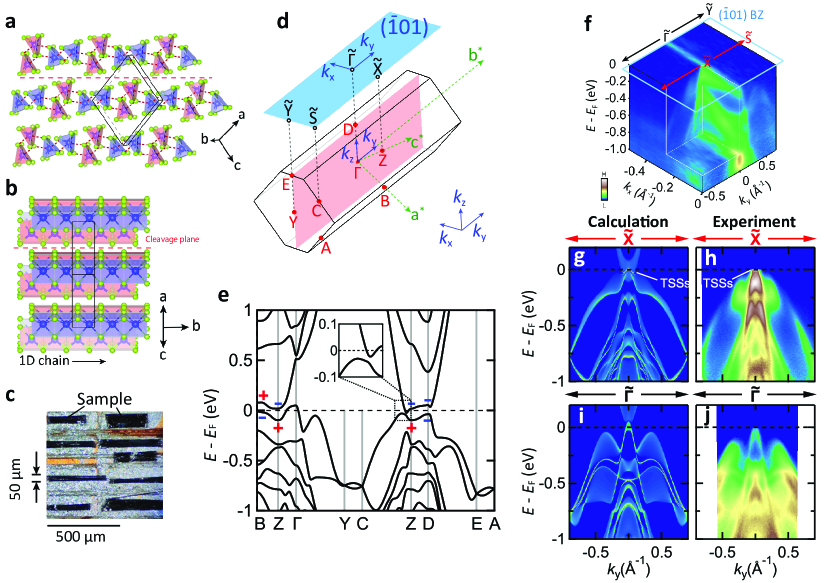
The crystal is built from the stacking of layers bonded together by the weak van der Waals force (Figs. 1a,b); this expects the plane to be left on the surface after the sample cleaving (Fig. 1c), which has indeed been confirmed by our X-ray diffraction measurements (see Supplementary Note \zrefSamples and Fig. \zrefXRDFig). The band structure calculated along high-symmetry momentum lines (see Fig. 1d) is plotted in Fig. 1e; band inversion occurs around the Z point, opening an energy gap induced by the SOC effect (the inset of Fig. 1e). We have used synchrotron-ARPES with tunable photon energies to experimentally clarify the overall electronic structure of . Figure 1f exhibits the overview of band dispersions observed on the surface Brillouin zone (BZ; see Fig. 1d). In Figs. 1g,h and Figs. 1i,j, we compare the calculated surface-state spectra (left panels) and ARPES dispersions (right panels) across the and points, respectively; a good agreement between the two is confirmed regardless of the momentum cuts.
The surface and bulk states have distinct spectral properties and can be selectively enhanced by using proper photon energies and light polarizations (see Supplementary Notes \zrefhvGamma,\zrefhvX and Figs. \zrefhvGammaFig,\zrefhvXFig). In Supplementary Figs. \zrefhvGammaFigm,n, we plot the Fermi surface mappings and the constant-energy mappings at a high binding energy (=0.6 eV), respectively, with different ’s accessed by changing the photon energies. Unlike the mapping at =0.6 eV, the Fermi surface is found to be non-dispersive along , suggesting that the low-energy sharp features seen in Fig. 1h very likely come from surface states. The TSSs are expected, by calculations, to be confined in a limited momentum area around the point and within a small bulk gap opened at ; thus, ultra-high energy and momentum resolutions are required in ARPES experiments to visualize the predicted TSSs, and most importantly, the spin-resolved measurements in high-resolutions are indispensable to identify that the surface states observed have indeed a topological origin.
TSSs and laser-ARPES.1TSSs and laser-ARPES.1\EdefEscapeHexTSSs and laser-ARPESTSSs and laser-ARPES\hyper@anchorstartTSSs and laser-ARPES.1\hyper@anchorend
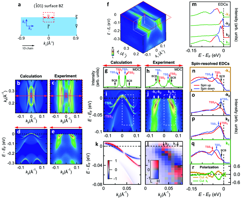
The fine details of the low-energy electronic structure near on the surface BZ has been examined at high-resolutions by a 7-eV laser-ARPES equipped with a 3D spin-resolved detector. Now we focus on the momentum area of a red dashed square in Fig. 2a surrounding the point; calculations predict that the TSSs, characterized by sharp spectra near , emerge between the bulk conduction and valence bands (BCB and BVB) when approaching the point, where these bands are inverted. In Figs. 2b,c and Figs. 2d,e, we compare the Fermi surfaces and dispersions across the point, respectively, obtained by calculations (left panels) and ARPES (right panels); the ARPES data are also three-dimensionally displayed in Fig. 2f for better understanding. The low-energy spectra measured by laser-ARPES (Figs. 2c,e,f) clearly disentangle fine structures near the point, which agree well with the calculated TSSs in the strong TI phase (Figs. 2b,d). To examine more details of the TSSs, we magnify the calculated and ARPES dispersions across in Figs. 2i,j, respectively. The momentum distribution curves (MDCs) extracted at (Figs. 2g,h) identify two pairs of TSSs (TSS1 and TSS2) and one pair of BCBs, indicating a good consistency between calculations and ARPES measurements. As detailed in Supplementary Fig. \zrefTSSBCBEDCsFig, the band dispersion of TSS1 goes up in energy with increasing and merges into the BCB around , whereas that of TSS2 goes down and merges into the BVB, just as expected for a strong TI phase (Fig. 2i). We also note here that spectra assigned to BCBs have relatively sharp peaks, unlike the continuum intensities for the surface band calculations (Fig. 2i), because of the following reason: ARPES at one photon energy, in principle, captures the band along a - sheet at a specific , thus it can exhibit sharp peaks in the spectra not only for the surface band but also for the bulk band, while the latter could be suppressed by the broadening in photoemission. This contrasts with the surface calculations, which project the bulk band spectra over the whole range of .
To finalize our conclusion that belongs to a strong TI phase, we demonstrate here that the surface states we observed are spin-polarized just as expected by calculations. For this purpose, the experimental setting is now switched to the spin-resolved mode. Figure 2l plots the SARPES data which map the spin component (slightly off from the direction in reality due to experimental geometry), measured for an energy-momentum region surrounded by a white box in Fig. 2j; one will see how high the momentum resolution is in laser-SARPES compared with that in synchrotron-ARPES (Fig. 1h). To examine more details, we extract, in Figs. 2n–q, the spin-resolved energy distribution curves (EDCs) at the four specific points indicated by arrows in Fig. 2j; the observed surface states are clearly spin-polarized (see Supplementary Fig. \zrefSpinComponentFig for the complete spin-polarization components). In Fig. 2r, the magnitude of spin-polarization is quantified for two outer points with opposite signs (+ and -). The spin-polarization is reversed both with different energies and between . Intriguingly, we also found that these relationships on reversal are also swapped between different ( and ), which yields a nodal point with spin degeneracy possibly due to the band hybridization of TSSs. Note here that, while the spectral intensities in Fig. 2o are dominated by the down spin (blue spectrum) mostly due to the matrix element effect, the spin degeneracy lifted by 10 meV is clearly resolved, validating the spin-texture reversal. For clarity, the conclusion experimentally obtained is summarized in Fig. 2m by painting the spin-integrated EDCs with red and blue colors assigned for up- and down-spin, respectively. All these features in the spin texture are well reproduced by calculations (Fig. 2k), justifying that our experiments successfully captured the spin-momentum locked TSSs, and hence established a strong TI phase in . We note that is not an insulator with a fully opened bulk gap in its strong TI phase, but a semimetal with a finite density of states at the Fermi level, which is a required condition to realize superconductivity making this compound all the more fascinating for the possible applications with topological superconductivity.
Strain-induced phase transitions.1Strain-induced phase transitions.1\EdefEscapeHexStrain-induced phase transitionsStrain-induced phase transitions\hyper@anchorstartStrain-induced phase transitions.1\hyper@anchorend
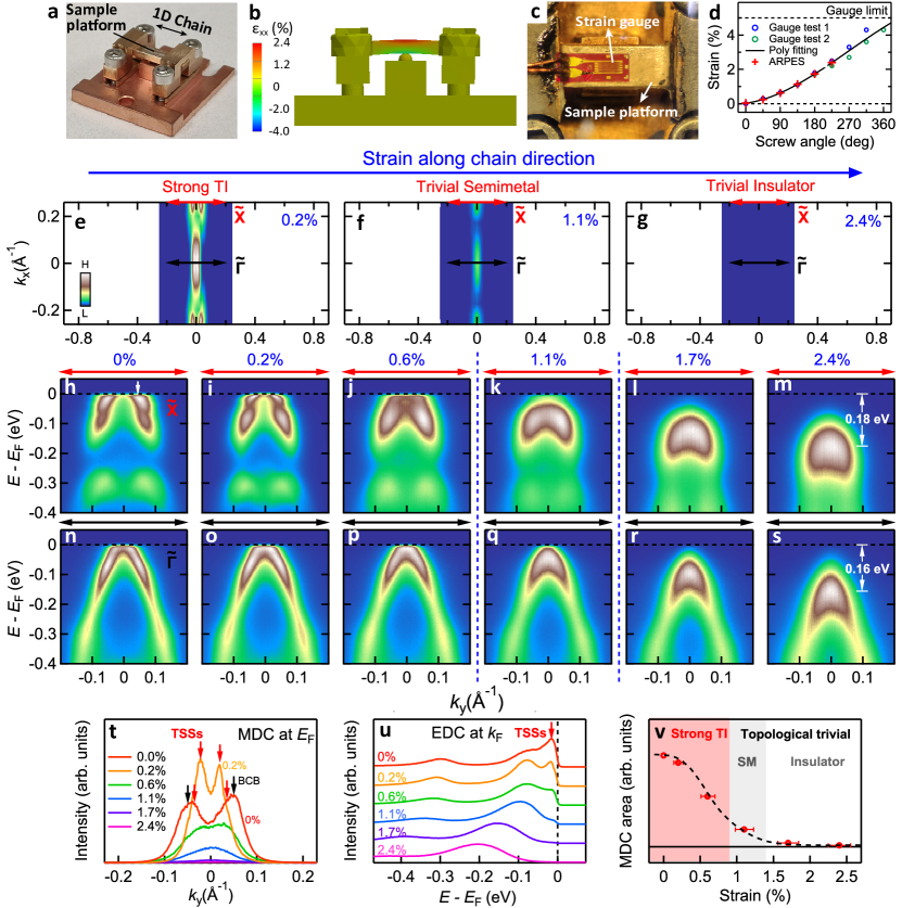
The quasi-1D structure is advantageous to modify the band structure effectively by uniaxial pressure. Hence, built from chains is the ideal material to realize the strain-induced topological phase transition. Here we use the simplest technique of applying pressure to substances, which just mechanically bends a crystal on a substrate (see Figs. 3a,b) [34], and reveal a systematic variation of the band structure under the tensile strain along the chain direction which is controlled -. The samples were mounted on the sample platform of the strain device shown in Fig. 3a, by which tensile strain is applied via tightening four screws (Fig. 3b). We measured the amount of strain at the sample position by commercial strain gauges (Fig. 3c), and made a diagram relating the turning angle of screws and the resulting strain (Fig. 3d), which was then used for the - strain control. The reliability of this diagram was evaluated by simulating the strain distribution in the device with finite element analysis (Fig. 3b); a good agreement has been confirmed between the simulation and the strain gauge measurements (see Methods for more information about the strain device and the estimation of the strain).
Figures 3e–g present the evolution of Fermi surface mappings by laser-ARPES with increasing tensile strain along the chain (0.2 , 1.1 , and 2.4 , respectively), signifying two-step phase transitions: the high intensities seen at low strain (Fig. 3e) are significantly suppressed by applying higher strain (Fig. 3f), indicating that the TSSs disappear and thus the system has transitioned from a strong TI phase to a trivial semimetal phase; its semimetallic nature will be confirmed by comparisons with calculations in Fig. 4 and Supplementary Fig. \zrefSemimetalFig. The vague intensities left for the bulk states (Fig. 3f) eventually vanish with further increase of the strain (Fig. 3g), revealing a transition of the system to a trivial band insulator phase, which opens a bulk gap at .
More details of these two-step phase transitions are examined in Figs. 3h–m and Figs. 3n–s, which exhibit the evolution of band dispersions across and (red and black arrows in Figs. 3e–g), respectively, with gradually increasing tensile strain along the chain by the - control. The highly intense signals due to TSSs are distinguished close to at zero strain (Fig. 3h) and agree to the results in Fig. 2e; the difference in the spectral sharpness between these data mostly comes from the different quality of cleaved surfaces and different light polarizations used in two different ARPES apparatuses each for the spin-texture and strain-control measurements (see Supplementary Figs. \zrefTSSs_XFig,\zrefTSSsAllFig for TSSs obtained at different conditions). By applying the tensile strain, the hole bands around and both gradually shifted toward higher binding energies, demonstrating successful band-engineering by strain. The key features associated with the phase transitions are seen especially in the close vicinity of around the point: the high intensities of TSSs seen at zero strain (Fig. 3h) were substantially suppressed at around 1 strain (Figs. 3j,k), which was then followed by a gap opening with larger strain (Figs. 3l,m). These behaviors are more directly demonstrated in Fig. 3t and Fig. 3u by extracting MDCs at across and EDCs at around , respectively, which reveal the spectral evolution of TSSs (marked by red arrows in these panels). As the strain was increased in the strong TI phase, the TSSs became confined into a smaller momentum area (Fig. 3t), as a result of the reduced band inversion. Further increase of strain caused the spectral peaks of TSSs to disappear by eliminating the band inversion, and consequently the system transitioned to a trivial semimetal phase. Eventually, the strain got large enough to reopen the band gap with totally vanishing the spectral intensity around , and thus the system transitioned to a trivial insulator phase. A previous study has shown an anomalous strain effect on the resistivity, which increased by several orders of magnitude when the applied strain along the chain reached 0.6% [35], in agreement with our observation of the band structure and the depletion of the spectral intensity at shown in Fig. 3v.
Calculations and discussions.1Calculations and discussions.1\EdefEscapeHexCalculations and discussionsCalculations and discussions\hyper@anchorstartCalculations and discussions.1\hyper@anchorend
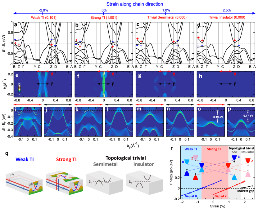
To fully understand the mechanism of the phase transitions we observed, calculations were performed for under the strain along the chain direction. The evolution of the bulk electronic structure in the calculations (Figs. 4b-d) nicely illustrates the mechanism of the phase transition induced by reducing and eliminating the band inversion with increasing tensile strain, which are manifested as the closing and reopening of a gap at the Z point. The calculated surface spectra of Fermi surface (Figs. 4f-h) and energy dispersions (Figs. 4k-p) across and both reproduce well our observations of two-step phase transitions from a strong TI phase to a trivial semimetal phase, and moreover to a trivial band insulator phase, with increasing the tensile strain up to 2.5 , which is comparable to the maximum strain value in our experiments; the spectral agreement between experimental observations (Figs. 3f,k,q in semimetal phase and Figs. 3g,m,s in insulator phase) and calculations (Figs. 4g,m,n and Figs. 4h,o,p, respectively) is excellent (see Supplementary Figs. \zrefSemimetalFig,\zrefInsulatorFig for direct comparisons).
We also calculated the effect of compressive strain on (Figs. 4a,e,i,j); it not only enlarges the band inversion at the Z point, but also inverts another band at the B point (Fig. 4a), triggering an additional topological phase transition from a strong TI phase to a weak TI phase, where the TSSs emerge only at the side surface (Fig. 4q). Applying compressive strain to quasi-1D crystals is experimentally very challenging since a compression in the chain direction easily bends or wrinkles the crystals, which releases the compressive force before reaching the amount we intended to apply. Even so, we have applied compressive strain to some extent and successfully observed the enhancement of band inversion, which indicates that the system was driven towards the weak TI phase by the compressive strain, as calculations predict (see Supplementary Figs. \zrefCompressiveStrainFig and \zrefCompressiveWTIFig); nevertheless, the decisive evidence for the weak TI phase is lacking, so we leave it for a future work.
In Fig. 4r, we summarize the evolution of the direct energy gaps at B and Z, and also the indirect gap of the system, with strain applied along the chain (), which determine the bulk topology and the metallic nature of , respectively. The topological quantum critical points have been obtained at -0.75 % and 0.95 %; the band inversion occurs both at B and Z for -0.75 %, and only at Z for -0.75 % 0.95 %, and eventually it is ruled out for 0.95 %, where a weak TI, a strong TI, and a trivial semimetal phase appear, respectively. Moreover, we also found another type of critical point at 1.75 %, across which the metal-insulator transition occurs. The correspondence between the values applied and the electronic phases obtained in calculations matches surprisingly well with our experimental results (Fig. 3v).
The strain-induced topological phase transition can be generally interpreted as follows. The tensile strain increases the distance among atoms building the crystal, which suppresses the hopping integral of electrons and thus shrinks the electronic bands. As a result, the overlapping of conduction and valence bands is diminished, and eventually, the band inversion is lifted with enough strain, causing the transition from the non-trivial topological phase to the trivial phase. The calculations in Figs. 4b-d clearly show that the valence bands are narrowed as tensile strain increases, lifting the band inversion and eventually opening the full band gap. The opposite occurs with the compressive strain (Fig. 4a): the electronic bands expand due to the larger hopping integral of electrons, which enhances the overlapping of conduction and valence bands. Consequently, another band inversion occurs, causing the transition from the strong TI phase to the weak TI phase.
The quasi-1D topological state of a superconductor we have revealed could have several different scientific and technological implications. In particular, has an excellent functionality in that the band topology is easily controlled by mechanical strain, leading to the reversible on/off switching of highly directional, dense spin currents that are protected against the impurity scattering (see Supplementary Fig. \zrefStrainControlFig for the reversibility). To date, the topological phase transition from a strong TI phase to a trivial insulator phase has been observed directly by ARPES for alloys, where the bulk topology is controlled by elemental substitution, which varies both the lattice constant and the SOC strength. A new way for it we have demonstrated here, which tunes only the lattice constant by strain, is much simpler, reversible, and thus promising for the future application. Hence, our experimental observations of the topological phase transition between a strong TI state and a trivial state realized in a superconductor will prompt further basic and technological researches for engineering the topological spintronics or optoelectronics which exploits the topological phase transition and the interplay of topological state with superconductivity likely leading to the topological superconducting state. While further works are required, the expectation for the availability to control the Majorana fermions would encourage follow-up researches on the new strategies for realizing quantum computation.
lofb
Methods.1Methods.1\EdefEscapeHexMethodsMethods\hyper@anchorstartMethods.1\hyper@anchorend Methods
Samples.2Samples.2\EdefEscapeHexSamplesSamples\hyper@anchorstartSamples.2\hyper@anchorend Samples
High-quality monoclinic whisker crystals of were synthesized by the vapor phase transport method, with a = 10.405 , b = 3.499 , c = 9.826 , and = 106.26 [36].
Typical samples used for the ARPES and SARPES measurements are shown in Fig. 1c with in-plane dimension 500 50 – 100 .
The samples used in the strain-dependent measurements were intentionally selected to be as small and thin as possible (generally 500 50 2 ), to diminish any strain relaxation effects.
More details can be found in Supplementary Note \zrefSamples.
ARPES.2ARPES.2\EdefEscapeHexARPESARPES\hyper@anchorstartARPES.2\hyper@anchorend ARPES
Synchrotron-based ARPES measurements were performed at the beamline 5-2 of Stanford Synchrotron Radiation Lightsource (SSRL) with tunable photon energies from 25 eV to 100 eV. The spot size was 0.04 (horizontal) 0.01 (vertical) and the equipped ScientaOmicron DA30L analyser enables a full access of the momentum space without sample rotation, both facilitating the measurements as the typical sample width was 50 – 100 . The light polarization used was linear vertical (along the analyser slit) with the overall energy resolution from 10 – 20 meV and angular resolution better than 0.2; see Supplementary Notes \zrefhvGamma,\zrefhvX and Figs. \zrefhvGammaFig,\zrefhvXFig for more detailed discussions about photon energy and light polarization dependences of the spectra. The samples were cleaved using exfoliation method and measured - at a temperature 10 K and a pressure better than Torr.
The laser-based SARPES [37] measurements were performed at the Institute for Solid State Physics, University of Tokyo, equipped with 6.994 eV photons and a ScientaOmicron DA30L analyser. The laser was -polarized with spot size 0.05 . See Supplementary Notes \zrefSpinComponent,\zrefSpinLaserPolarization and Figs. \zrefSpinComponentFig,\zrefSpinLaserPolarizationFig for more information about the laser polarizations and apparatus geometry. The energy (angular) resolution was set at better than 2 meV (0.2 ) and 15 meV (0.7) for ARPES and SARPES, respectively. The samples were cleaved using similar method at room temperature with a pressure better than Torr and measured at 10 K with a pressure better than Torr. The spin-polarization map in Fig. 2l utilizes a 2D color coding with horizontal and vertical axes indicating the spectral weight and the polarization, respectively [38, 39].
The strain-dependent laser-ARPES measurements were performed in similar conditions to SARPES but with a ScientaOmicron R4000 analyser. The angular resolution was 0.3 and the laser polarization was linear horizontal (along the analyser slit). More information about laser polarizations and apparatus geometry is shown in Supplementary Fig. \zrefhvGammaFig. The samples were mounted on the strain device using silver epoxy (Muromac H-220), cleaved - at room temperature with a pressure better than Torr, and measured at a temperature 10 K with a pressure Torr. The - strain controls were realized by rotating the screws 45 step by step at a temperature 30 K with a pressure better than Torr. Typical time for one 45 rotation was 2 minutes and we confirmed no surface aging by performing strain control cycles and measuring at freshly cleaved samples with strain applied ex-situ (Supplementary Fig. \zrefStrainControlFig). We also show the - strain-control reversibility test in Supplementary Fig. \zrefStrainControlFig, the results indicate the strain effects are completely reversible. After each measurement, we monitored the device status, estimated and calibrated the - controlled strain magnitude to the strain measured by the strain gauges, as described below.
Strain evaluation.2Strain evaluation.2\EdefEscapeHexStrain evaluationStrain evaluation\hyper@anchorstartStrain evaluation.2\hyper@anchorend Strain evaluation
The strain device [34] was specially designed for the low-energy laser-ARPES apparatus. The key components of the device include two BeCu bridges, one BeCu sample platform (10 2 1 ), and one ball (1 diameter) below it. When the screws are tightened, the sample platform is bended by the bridges providing uniaxial strain to the samples mounted, as demonstrated in Fig. 3b. As the laser spot size is small, we found no evidence of spectral broadening due to possible domains introduced by bending. Good thermal (electric) conductivity has been confirmed by comparing the spectra with those obtained from samples mounted on normal sample holders.
The strain magnitude as a function of screw angles (Fig. 3d) was measured by the commercial strain gauges (Fig. 3c, KYOWA KFGS-1N-120-C1-11) at room temperature. For both the strain gauge measurements and the strain-dependent ARPES measurements, we always carefully adjusted the screws and platforms to ensure the initial conditions of the devices were identical within error bars: before the measurements, the heights of the fours screws and the bridges were equally adjusted to ensure a flat platform; meanwhile, the displacements between the center of the sample platform and its contact positions with the bridges were carefully monitored, so that a zero net strain was ensured before attaching the strain gauges or mounting samples. We have conducted several strain gauge measurements on different devices and obtained similar results (two of them are shown in Fig. 3d). By fitting the data with a polynomial function (the red curve in Fig. 3d), we can then estimate the strain magnitude - controlled during the ARPES measurements by interpolating at the corresponding screw angles. We also measured the displacements as a function of the strain, as shown in Supplementary Fig. \zrefStrainDeviceFigd. Comparing to the large strain in our experiments ( 2.4%), we ignore the thermal contraction which is typically -0.2% according to our thermal-strain simulations. The error bars for the strain magnitude controlled in the ARPES measurements were estimated in accordance with the uncertainty of screw angles and shown in Figs. 3d,v (smaller than the marker size in Fig. 3d).
The strain simulations based on finite element analysis were performed when the platform displacement reached 0.124 (Supplementary Figs. \zrefStrainDeviceFigd,g), using the Autodesk Inventor 2020. For the BeCu components, a Young’s modulus of 120 GPa and a Poisson’s ratio of 0.3 were implemented. Figure 3b and Supplementary Fig. \zrefStrainDeviceFige show the simulated axial strain () distribution on the sample platform. reached the maximum 2.4% at the platform center, nicely consistent with our experimental results from the strain gauges at the same displacement (Supplementary Fig. \zrefStrainDeviceFigd). The transverse strain () distribution is shown in Supplementary Fig. \zrefStrainDeviceFigf, which reached the minimum -0.2% at the platform center. Supplementary Fig. \zrefStrainDeviceFigh summarizes the overall strain distribution by plotting the and as a function of coordinates along x (y = 0) and along y (x = 0), respectively. We note that the samples used for strain-dependent ARPES measurements were very small (generally 500 50 2 ) and mounted at the center of the platform. Therefore, the tiny transverse strain perpendicular to the platform is neglectable. Moreover, as the samples used were also very thin, our simulations show that the strain on the sample surface was almost the same as that on the platform center (Supplementary Figs. \zrefStrainDeviceFigi,j). See Supplementary Notes \zrefStrainDevice,\zrefStrainControl for more detailed descriptions about the strain devices, strain evaluation, and - strain controls.
Calculations.2Calculations.2\EdefEscapeHexCalculationsCalculations\hyper@anchorstartCalculations.2\hyper@anchorend DFT Calculations
First, we performed the structural optimization using the Perdew-Burke-Ernzerhof exchange-correlation functional revised for solids [40] and the projector augmented wave method [41] as implemented in Vienna ab initio Simulation Package [42, 43, 44, 45]. The spin-orbit coupling was included in all the calculations presented in this paper. Here, we optimized atomic coordinates while the lattice parameters were fixed as our experimental values. We also optimized atomic coordinates in strain calculations, where the lattice parameters except for (the length along the strain direction) were fixed as unstrained values for simplicity. Next, we performed first-principles band-structure calculation using the modified Becke-Johnson potential [46] as implemented in the WIEN2k code [47]. The muffin-tin radii for Ta and Se were set to 2.5 and 2.39 a.u., respectively, for the unstrained calculation while they are slightly changed for the strain calculations. The maximum modulus for the reciprocal lattice vectors was chosen so that . We took a 4124 -mesh for a self-consistent-field (SCF) calculation, while a following non-SCF calculation to determine the Fermi energy was performed using a finer -mesh up to 25,000 points. From the calculated band structures, we extracted the Wannier functions of the Ta- and Se- orbitals using the Wien2Wannier and Wannier90 codes [48, 49, 50, 51]. We did not perform the maximal localization procedure for the Wannier functions to prevent orbital mixing among the different spin components. The semi-infinite-slab tight-binding models constructed from these Wannier functions were used for calculating the surface spectra in the way described in Ref. 52. The Fermi energy in all the calculated data is shifted by -10 meV so as to reproduce the experimental spectra.
The tensile strain along the chain direction leads to finite compressive strain perpendicular to it due to the Poisson effect. However, we did not take the perpendicular compressive strain into account in the DFT calculations of Fig. 4 since the effect is negligible and not crucial for our conclusions. To confirm this, we have performed a simulation considering the Poisson’s ratio and estimated the perpendicular strain to be only -0.2% when the tensile strain along the chain direction was set to 2.4% (Supplementary Fig. \zrefStrainDeviceFigh), which is the maximum value we applied for the samples in our experiments. Subsequently, we calculated the bulk band structure under the 2.4% tensile strain along the chain direction with and without the effect of the perpendicular compressive strain of -0.2%; no considerable difference was obtained between the two (Supplementary Fig. \zrefBulkCalcPoissonFig), leading us to conclude that the effect of the perpendicular compressive stain can be ignored in our study.
Data availability
The data that support the findings of this study are available from the corresponding author upon request.
Acknowledgements
We thank D. Hirai and Y. Mizukami for fruitful comments on the strain measurements, and also thank S. Sakuragi and T. Yajima for XRD measurements. Use of the Stanford Synchrotron Radiation Lightsource, SLAC National Accelerator Laboratory, is supported by the U.S. Department of Energy, Office of Science, Office of Basic Energy Sciences under Contract No. DE-AC02-76SF00515. This work was supported by the JSPS KAKENHI (grant numbers JP18H01165, JP18K03484, JP19H02683, JP19F19030 and JP19H00651), MEXT Q-LEAP (grant number JPMXS0118068681), and by MEXT under the “Program for Promoting Researches on the Supercomputer Fugaku” (Basic Science for Emergence and Functionality in Quantum Matter Innovative Strongly Correlated Electron Science by Integration of “Fugaku” and Frontier Experiments) (Project ID: hp200132).
Author contributions
T.K. and S.T. planned the experimental project. C.L. conducted ARPES experiments, analysed the data, and performed strain simulations. C.L. and T.K. designed the strain devices. C.L. Ke.K, Y.A., and T.K. conducted strain gauge measurements. R.N., Ke.K., P.Z., C.B., Ki.K., Y.A., Ka.K., H.T., K.Y., A.H., M.H., D.L., S.S., and T.K. supported ARPES experiment. M.S., A.N., M.T., and S.T. prepared the single crystals. M.O. and R.A. calculated and analyzed the theoretical band structure. C.L., M.O., and T.K. wrote the paper. All authors discussed the results and commented on the manuscript.
Competing interests
The authors declare no competing interests.
Additional information
Correspondence and requests for materials should be addressed to T.K. (email: kondo1215@issp.u-tokyo.ac.jp).
References
- Fu et al. [2007] L. Fu, C. L. Kane, and E. J. Mele, Topological Insulators in Three Dimensions, Phys. Rev. Lett. 98, 106803 (2007).
- Fu and Kane [2007] L. Fu and C. L. Kane, Topological insulators with inversion symmetry, Phys. Rev. B 76, 045302 (2007).
- Hasan and Kane [2010] M. Z. Hasan and C. L. Kane, Colloquium: Topological insulators, Rev. Mod. Phys. 82, 3045 (2010).
- Qi and Zhang [2011] X.-L. Qi and S.-C. Zhang, Topological insulators and superconductors, Rev. Mod. Phys. 83, 1057 (2011).
- Ando [2013] Y. Ando, Topological Insulator Materials, J. Phys. Soc. Jpn. 82, 102001 (2013).
- Xu et al. [2011] S.-Y. Xu, Y. Xia, L. A. Wray, S. Jia, F. Meier, J. H. Dil, J. Osterwalder, B. Slomski, A. Bansil, H. Lin, R. J. Cava, and M. Z. Hasan, Topological Phase Transition and Texture Inversion in a Tunable Topological Insulator, Science 332, 560 (2011).
- Sato et al. [2011] T. Sato, K. Segawa, K. Kosaka, S. Souma, K. Nakayama, K. Eto, T. Minami, Y. Ando, and T. Takahashi, Unexpected mass acquisition of Dirac fermions at the quantum phase transition of a topological insulator, Nat. Phys. 7, 840 (2011).
- Xu et al. [2012] S.-Y. Xu, C. Liu, N. Alidoust, M. Neupane, D. Qian, I. Belopolski, J. D. Denlinger, Y. J. Wang, H. Lin, L. A. Wray, G. Landolt, B. Slomski, J. H. Dil, A. Marcinkova, E. Morosan, Q. Gibson, R. Sankar, F. C. Chou, R. J. Cava, A. Bansil, and M. Z. Hasan, Observation of a topological crystalline insulator phase and topological phase transition in Pb1-xSnxTe, Nat. Commun. 3, 1 (2012).
- Brahlek et al. [2012] M. Brahlek, N. Bansal, N. Koirala, S.-Y. Xu, M. Neupane, C. Liu, M. Z. Hasan, and S. Oh, Topological-Metal to Band-Insulator Transition in Thin Films, Phys. Rev. Lett. 109, 186403 (2012).
- Zhang et al. [2013] J. Zhang, C.-Z. Chang, P. Tang, Z. Zhang, X. Feng, K. Li, L.-l. Wang, X. Chen, C. Liu, W. Duan, K. He, Q.-K. Xue, X. Ma, and Y. Wang, Topology-Driven Magnetic Quantum Phase Transition in Topological Insulators, Science 339, 1582 (2013).
- Wu et al. [2013] L. Wu, M. Brahlek, R. Valdés Aguilar, A. V. Stier, C. M. Morris, Y. Lubashevsky, L. S. Bilbro, N. Bansal, S. Oh, and N. P. Armitage, A sudden collapse in the transport lifetime across the topological phase transition in (Bi1-xInx)2Se3, Nat. Phys. 9, 410 (2013).
- Xu et al. [2015] S.-Y. Xu, M. Neupane, I. Belopolski, C. Liu, N. Alidoust, G. Bian, S. Jia, G. Landolt, B. Slomski, J. H. Dil, P. P. Shibayev, S. Basak, T.-R. Chang, H.-T. Jeng, R. J. Cava, H. Lin, A. Bansil, and M. Z. Hasan, Unconventional transformation of spin Dirac phase across a topological quantum phase transition, Nat. Commun. 6, 6870 (2015).
- Monceau [2012] P. Monceau, Electronic crystals: An experimental overview, Adv. Phys. 61, 325 (2012).
- Sambongi et al. [1977] T. Sambongi, M. Yamamoto, K. Tsutsumi, Y. Shiozaki, K. Yamaya, and Y. Abe, Superconductivity in One-Dimensional TaSe3, J. Phys. Soc. Jpn. 42, 1421 (1977).
- Stolyarov et al. [2016] M. A. Stolyarov, G. Liu, M. A. Bloodgood, E. Aytan, C. Jiang, R. Samnakay, T. T. Salguero, D. L. Nika, S. L. Rumyantsev, M. S. Shur, K. N. Bozhilov, and A. A. Balandin, Breakdown current density in h-BN-capped quasi-1D TaSe3 metallic nanowires: Prospects of interconnect applications, Nanoscale 8, 15774 (2016).
- Liu et al. [2017] G. Liu, S. Rumyantsev, M. A. Bloodgood, T. T. Salguero, M. Shur, and A. A. Balandin, Low-Frequency Electronic Noise in Quasi-1D TaSe3 van der Waals Nanowires, Nano Lett. 17, 377 (2017).
- Nie et al. [2018] S. Nie, L. Xing, R. Jin, W. Xie, Z. Wang, and F. B. Prinz, Topological phases in the compound, Phys. Rev. B 98, 125143 (2018).
- Fu and Berg [2010] L. Fu and E. Berg, Odd-Parity Topological Superconductors: Theory and Application to , Phys. Rev. Lett. 105, 097001 (2010).
- Sasaki et al. [2011] S. Sasaki, M. Kriener, K. Segawa, K. Yada, Y. Tanaka, M. Sato, and Y. Ando, Topological Superconductivity in , Phys. Rev. Lett. 107, 217001 (2011).
- Wang et al. [2012] M.-X. Wang, C. Liu, J.-P. Xu, F. Yang, L. Miao, M.-Y. Yao, C. L. Gao, C. Shen, X. Ma, X. Chen, Z.-A. Xu, Y. Liu, S.-C. Zhang, D. Qian, J.-F. Jia, and Q.-K. Xue, The Coexistence of Superconductivity and Topological Order in the Bi2Se3 Thin Films, Science 336, 52 (2012).
- Mourik et al. [2012] V. Mourik, K. Zuo, S. M. Frolov, S. R. Plissard, E. P. a. M. Bakkers, and L. P. Kouwenhoven, Signatures of Majorana Fermions in Hybrid Superconductor-Semiconductor Nanowire Devices, Science 336, 1003 (2012).
- Sakano et al. [2015] M. Sakano, K. Okawa, M. Kanou, H. Sanjo, T. Okuda, T. Sasagawa, and K. Ishizaka, Topologically protected surface states in a centrosymmetric superconductor -PdBi 2, Nat. Commun. 6, 8595 (2015).
- Guan et al. [2016] S.-Y. Guan, P.-J. Chen, M.-W. Chu, R. Sankar, F. Chou, H.-T. Jeng, C.-S. Chang, and T.-M. Chuang, Superconducting topological surface states in the noncentrosymmetric bulk superconductor PbTaSe2, Sci. Adv. 2, e1600894 (2016).
- Zhang et al. [2018] P. Zhang, K. Yaji, T. Hashimoto, Y. Ota, T. Kondo, K. Okazaki, Z. Wang, J. Wen, G. D. Gu, H. Ding, and S. Shin, Observation of topological superconductivity on the surface of an iron-based superconductor, Science 360, 182 (2018).
- Clark et al. [2018] O. J. Clark, M. J. Neat, K. Okawa, L. Bawden, I. Marković, F. Mazzola, J. Feng, V. Sunko, J. M. Riley, W. Meevasana, J. Fujii, I. Vobornik, T. K. Kim, M. Hoesch, T. Sasagawa, P. Wahl, M. S. Bahramy, and P. D. C. King, Fermiology and Superconductivity of Topological Surface States in , Phys. Rev. Lett. 120, 156401 (2018).
- Liu et al. [2020] W. Liu, L. Cao, S. Zhu, L. Kong, G. Wang, M. Papaj, P. Zhang, Y.-B. Liu, H. Chen, G. Li, F. Yang, T. Kondo, S. Du, G.-H. Cao, S. Shin, L. Fu, Z. Yin, H.-J. Gao, and H. Ding, A new Majorana platform in an Fe-As bilayer superconductor, Nat. Commun. 11, 5688 (2020).
- Yuan et al. [2019] Y. Yuan, J. Pan, X. Wang, Y. Fang, C. Song, L. Wang, K. He, X. Ma, H. Zhang, F. Huang, W. Li, and Q.-K. Xue, Evidence of anisotropic Majorana bound states in 2M-WS2, Nat. Phys. 15, 1046 (2019).
- Perucchi et al. [2004] A. Perucchi, C. Søndergaard, S. Mitrovic, M. Grioni, N. Barisic, H. Berger, L. Forró, and L. Degiorgi, Spectroscopic and dc-transport investigations of the electronic properties of , Eur. Phys. J. B 39, 433 (2004).
- Chen et al. [2020] C. Chen, A. Liang, S. Liu, S. Nie, J. Huang, M. Wang, Y. Li, D. Pei, H. Yang, H. Zheng, Y. Zhang, D. Lu, M. Hashimoto, A. Barinov, C. Jozwiak, A. Bostwick, E. Rotenberg, X. Kou, L. Yang, Y. Guo, Z. Wang, H. Yuan, Z. Liu, and Y. Chen, Observation of Topological Electronic Structure in Quasi-1D Superconductor TaSe3, Matter 3, 2055 (2020).
- Flötotto et al. [2018] D. Flötotto, Y. Bai, Y.-H. Chan, P. Chen, X. Wang, P. Rossi, C.-Z. Xu, C. Zhang, J. A. Hlevyack, J. D. Denlinger, H. Hong, M.-Y. Chou, E. J. Mittemeijer, J. N. Eckstein, and T.-C. Chiang, In Situ Strain Tuning of the Dirac Surface States in Bi2Se3 Films, Nano Lett. 18, 5628 (2018).
- Kostylev et al. [2020] I. Kostylev, S. Yonezawa, Z. Wang, Y. Ando, and Y. Maeno, Uniaxial-strain control of nematic superconductivity in SrxBi2Se3, Nat. Commun. 11, 4152 (2020).
- Mutch et al. [2019] J. Mutch, W.-C. Chen, P. Went, T. Qian, I. Z. Wilson, A. Andreev, C.-C. Chen, and J.-H. Chu, Evidence for a strain-tuned topological phase transition in ZrTe5, Sci. Adv. 5, eaav9771 (2019).
- Zhang et al. [2021] P. Zhang, R. Noguchi, K. Kuroda, C. Lin, K. Kawaguchi, K. Yaji, A. Harasawa, M. Lippmaa, S. Nie, H. Weng, V. Kandyba, A. Giampietri, A. Barinov, Q. Li, G. D. Gu, S. Shin, and T. Kondo, Observation and control of the weak topological insulator state in ZrTe5, Nat. Commun. 12, 406 (2021).
- Riccò et al. [2018] S. Riccò, M. Kim, A. Tamai, S. M. Walker, F. Y. Bruno, I. Cucchi, E. Cappelli, C. Besnard, T. K. Kim, P. Dudin, M. Hoesch, M. J. Gutmann, A. Georges, R. S. Perry, and F. Baumberger, In situ strain tuning of the metal-insulator-transition of Ca2RuO4 in angle-resolved photoemission experiments, Nat. Commun. 9, 1 (2018).
- Tritt et al. [1986] T. M. Tritt, E. P. Stillwell, and M. J. Skove, Effect of uniaxial stress on the transport properties of , Phys. Rev. B 34, 6799 (1986).
- Nomura et al. [2017] A. Nomura, K. Yamaya, S. Takayanagi, K. Ichimura, T. Matsuura, and S. Tanda, Emergence of a resistance anomaly by Cu-doping in TaSe3, EPL 119, 17005 (2017).
- Yaji et al. [2016] K. Yaji, A. Harasawa, K. Kuroda, S. Toyohisa, M. Nakayama, Y. Ishida, A. Fukushima, S. Watanabe, C. Chen, F. Komori, and S. Shin, High-resolution three-dimensional spin- and angle-resolved photoelectron spectrometer using vacuum ultraviolet laser light, Rev. Sci. Instrum. 87, 053111 (2016).
- Tusche et al. [2015] C. Tusche, A. Krasyuk, and J. Kirschner, Spin resolved bandstructure imaging with a high resolution momentum microscope, Ultramicroscopy Special Issue: LEEM-PEEM 9, 159, 520 (2015).
- Noguchi et al. [2017] R. Noguchi, K. Kuroda, K. Yaji, K. Kobayashi, M. Sakano, A. Harasawa, T. Kondo, F. Komori, and S. Shin, Direct mapping of spin and orbital entangled wave functions under interband spin-orbit coupling of giant Rashba spin-split surface states, Phys. Rev. B 95, 041111 (2017).
- Perdew et al. [2008] J. P. Perdew, A. Ruzsinszky, G. I. Csonka, O. A. Vydrov, G. E. Scuseria, L. A. Constantin, X. Zhou, and K. Burke, Restoring the Density-Gradient Expansion for Exchange in Solids and Surfaces, Phys. Rev. Lett. 100, 136406 (2008).
- Kresse and Joubert [1999] G. Kresse and D. Joubert, From ultrasoft pseudopotentials to the projector augmented-wave method, Phys. Rev. B 59, 1758 (1999).
- Kresse and Hafner [1993] G. Kresse and J. Hafner, Ab initio molecular dynamics for liquid metals, Phys. Rev. B 47, 558 (1993).
- Kresse and Hafner [1994] G. Kresse and J. Hafner, Ab initio molecular-dynamics simulation of the liquid-metal–amorphous-semiconductor transition in germanium, Phys. Rev. B 49, 14251 (1994).
- Kresse and Furthmüller [1996a] G. Kresse and J. Furthmüller, Efficiency of ab-initio total energy calculations for metals and semiconductors using a plane-wave basis set, Comput. Mater. Sci. 6, 15 (1996a).
- Kresse and Furthmüller [1996b] G. Kresse and J. Furthmüller, Efficient iterative schemes for ab initio total-energy calculations using a plane-wave basis set, Phys. Rev. B 54, 11169 (1996b).
- Tran and Blaha [2009] F. Tran and P. Blaha, Accurate Band Gaps of Semiconductors and Insulators with a Semilocal Exchange-Correlation Potential, Phys. Rev. Lett. 102, 226401 (2009).
- Blaha et al. [2018] P. Blaha, K. Schwarz, G. K. H. Madsen, D. Kvasnicka, J. Luitz, R. Laskowsk, F. Tran, and L. D. Marks, WIEN2k: An Augmented Plane Wave + Local Orbitals Program for Calculating Crystal Properties (Karlheinz Schwarz, Techn. Universität Wien, Austria, 2018).
- Marzari and Vanderbilt [1997] N. Marzari and D. Vanderbilt, Maximally localized generalized Wannier functions for composite energy bands, Phys. Rev. B 56, 12847 (1997).
- Souza et al. [2001] I. Souza, N. Marzari, and D. Vanderbilt, Maximally localized Wannier functions for entangled energy bands, Phys. Rev. B 65, 035109 (2001).
- Kuneš et al. [2010] J. Kuneš, R. Arita, P. Wissgott, A. Toschi, H. Ikeda, and K. Held, Wien2wannier: From linearized augmented plane waves to maximally localized Wannier functions, Computer Physics Communications 181, 1888 (2010).
- Pizzi et al. [2020] G. Pizzi, V. Vitale, R. Arita, S. Blügel, F. Freimuth, G. Géranton, M. Gibertini, D. Gresch, C. Johnson, T. Koretsune, J. Ibañez-Azpiroz, H. Lee, J.-M. Lihm, D. Marchand, A. Marrazzo, Y. Mokrousov, J. I. Mustafa, Y. Nohara, Y. Nomura, L. Paulatto, S. Poncé, T. Ponweiser, J. Qiao, F. Thöle, S. S. Tsirkin, M. Wierzbowska, N. Marzari, D. Vanderbilt, I. Souza, A. A. Mostofi, and J. R. Yates, Wannier90 as a community code: New features and applications, J. Phys.: Condens. Matter 32, 165902 (2020).
- Sancho et al. [1985] M. P. L. Sancho, J. M. L. Sancho, J. M. L. Sancho, and J. Rubio, Highly convergent schemes for the calculation of bulk and surface Green functions, J. Phys. F: Met. Phys. 15, 851 (1985).