Radiative control of localized excitons at room temperature with an ultracompact tip-enhanced plasmonic nano-cavity
Abstract
In atomically thin semiconductors, localized exciton (XL) coupled to light shows single quantum emitting behaviors through radiative relaxation processes providing a new class of optical sources for potential applications in quantum communication. In most studies, however, XL photoluminescence (PL) from crystal defects has mainly been observed in cryogenic conditions because of their sub-wavelength emission region and low quantum yield at room temperature. Furthermore, engineering the radiative relaxation properties, e.g., emission region, intensity, and energy, remained challenging. Here, we present a plasmonic antenna with a triple-sharp-tips geometry to induce and control the XL emission of a WSe2 monolayer (ML) at room temperature. By placing a ML crystal on the two sharp Au tips in a bowtie antenna fabricated through cascade domino lithography with a radius of curvature of 1 nm, we effectively induce tensile strain in the nanoscale region to create robust XL states. An Au tip with tip-enhanced photoluminescence (TEPL) spectroscopy is then added to the strained region to probe and control the XL emission [1]. With TEPL enhancement of XL as high as in the triple-sharp-tips device, experimental results demonstrate the controllable XL emission in 30 nm area with a PL energy shift up to 40 meV, resolved by tip-enhanced PL and Raman imaging with 15 nm spatial resolution. Our approach provides a systematic way to control localized quantum light in 2D semiconductors offering new strategies for active quantum nano-optical devices.
keywords:
Single quantum emitter, localized exciton, tip-enhanced photoluminescence, plasmonic structures, nano-cavity, Purcell effectHyeongwoo Lee† Inki Kim† Chulho Park Mingu Kang Jungho Mun Yeseul Kim Markus B. Raschke Mun Seok Jeong Junsuk Rho∗ Kyoung-Duck Park∗
H. Lee, M. Kang, Prof. K.-D. Park
Department of Physics, Ulsan National Institute of Science and Technology (UNIST), Ulsan 44919, Republic of Korea
Email Address: kdpark@unist.ac.kr
I. Kim, Y. Kim, Prof. J. Rho
Department of Mechanical Engineering, Pohang University of Science and Technology (POSTECH), Pohang 37673, Republic of Korea
J. Mun, Prof. J. Rho
Department of Chemical Engineering, Pohang University of Science and Technology (POSTECH), Pohang 37673, Republic of Korea
C. Park, Prof. M.S. Jeong
Department of Energy Science, Sungkyunkwan University (SKKU), Suwon 16419, Republic of Korea
Prof. M.B. Raschke
Department of Physics, Department of Chemistry, and JILA, University of Colorado, Boulder, CO 80309, USA
1 Introduction
Ever since photoluminesence (PL) responses of localized exciton (XL) were observed in naturally occurring crystal defects and edges in atomically thin semiconductors [2, 3, 4, 5, 6, 7], their unique single quantum emitting behaviors in a fascinating 2D platform have attracted a lot of attentions for their potential applications in quantum information and communication devices [8, 9, 10]. In addition, recent studies have demonstrated that the XL can be deterministically induced at any desired locations. For instance, the XL emission was observed by transferring atomically thin semiconductors on nano-structures through the induced artificial strain [11, 12, 13]. Furthermore, a nanocube cavity array was exploited to induce strain and drive more efficient XL emission through Purcell enhancement [14], yet without the ability to control their radiative emission properties. As further practical applications, experiments inducing XL with nano-structures and controlling its frequency through actuators were reported [15, 16].
However, these studies have only been performed at cryogenic temperatures because of the small exciton binding energy of XL [17], which leads to a much lower quantum yield at room temperature compared to the overwhelming radiative emission of neutral exciton (X0) [18, 19]. Since these low temperature operations heavily restrict the practical application of single quantum emitting devices, there have been significant efforts to observe the XL emission at room temperature. To probe the weak XL emission at room temperature, local near-field PL measurements are the only possible approach up to the present. For instance, the defect bound excitons in a WS2 monolayer were spatially resolved using a near-field scanning optical microscopy (NSOM) with 70 nm spatial resolution [20]. In this work, it was found that the XL emission properties are strongly modulated by the structural features of the crystal defects. In addition, the strain-induced XL emissions at nanobubbles were probed using a scattering type NSOM approach [21]. Through higher spatial resolution (34 nm) nano-imaging and -spectroscopy, they revealed the correlation between the XL emission properties and the strain-induced confinement potential distribution with the support of a theoretical model. However, these near-field probing methods have low optical sensitivity and cannot artificially induce and control the XL emission. Therefore, it is highly desirable to deterministically induce, probe, and control the XL emission with high optical sensitivity and nanoscale spatial resolution at room temperature.
Here, we present a dynamic plasmonic nano-cavity combined with tip-enhanced nano-spectroscopy to deterministically induce, locally probe, and systematically control the XL emission at room temperature. We facilitate the localized states of excitons in a WSe2 monolayer by inducing a tensile strain on the nanoscale using extremely sharp bowtie tips [22]. We then form the triple-sharp-tips plasmonic cavity by adding an Au tip on the bowtie nano-gap and measuring tip-enhanced photoluminescence (TEPL) of the XL with spatial resolution of 15 nm. In this case, the radiative emission rate of the XL is highly enhanced by the Purcell effect in the ultracompact cavity [23, 24, 25] and we achieve 106-fold TEPL enhancement. In addition, we can dynamically tune the cavity mode volume and the corresponding excitation field strength and emission rate through the atomic force control of the Au tip with 0.2 nm precision [26], which enables the radiative control of XL.
2 Results
2.1 Triple-sharp-tips geometry for deterministic localized exciton emission
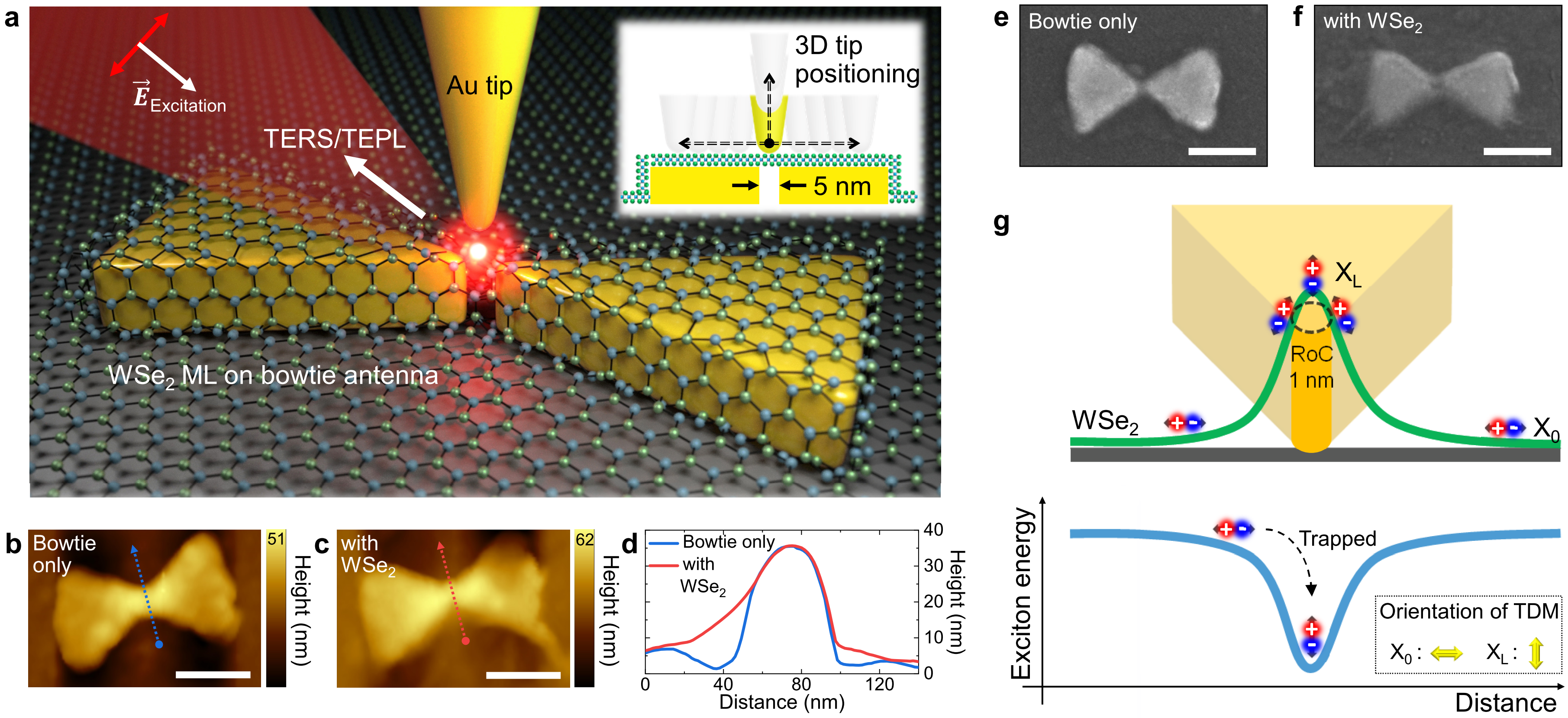
To induce artificial nanoscale strain in WSe2 monolayer (ML), we use sharp tips in an Au bowtie structure fabricated by cascade domino lithography, which overcomes long-standing challenge of sub-nanometer tip fabrication [22]. The tips in the bowtie structure then has a 5 nm gap with a radius of curvature (RoC) of 1 nm. When the WSe2 ML is transferred to this extremely sharp structure, the locally induced strain forms a potential well, which can bound excitons tightly on the nanoscale [27, 28, 12]. To couple optical fields effectively to these XL and detect their PL responses, we use TEPL spectroscopy, as illustrated in Figure 1a [29]. The electrochemically etched Au tip is positioned on the nano-gap to form the triple-sharp-tips geometry and able to control the distance between tip and sample with 0.2 nm precision using shear-force atomic force microscopy (AFM) feedback (see Experimental Section for details).
When a linearly polarized excitation beam (632.8 nm), polarized parallel with respect to the tip axis, is focused onto the triple-sharp-tips structure, both in-plane and out-of-plane optical fields are strongly localized which enable us to measure TEPL response of X0 and XL. We confirm the capping condition of the transferred crystal on the nano-gap through AFM and scanning electron microscopy (SEM) measurements, as shown in Figure 1b-f. As can be seen in the high-resolution 2D images and topographic line profiles, the ML crystal uniformly covers the bowtie structure and forms a stiff curve at the nano-gap. Figure 1g (top) shows an illustration of the steeply curved WSe2 ML formed by the extremely sharp tips of the bowtie antenna. Since the strain is induced in the nanoscale steep curve, neutral excitons drift and are bound to the confinement potential as a form of the localized state [21]. Specifically, a tensile strain is strongly induced into the vertical axis which decreases the energy state of the XL as described in Figure 1g (bottom).
2.2 Nano-chemical characterization of the structure of transferred WSe2 monolayer
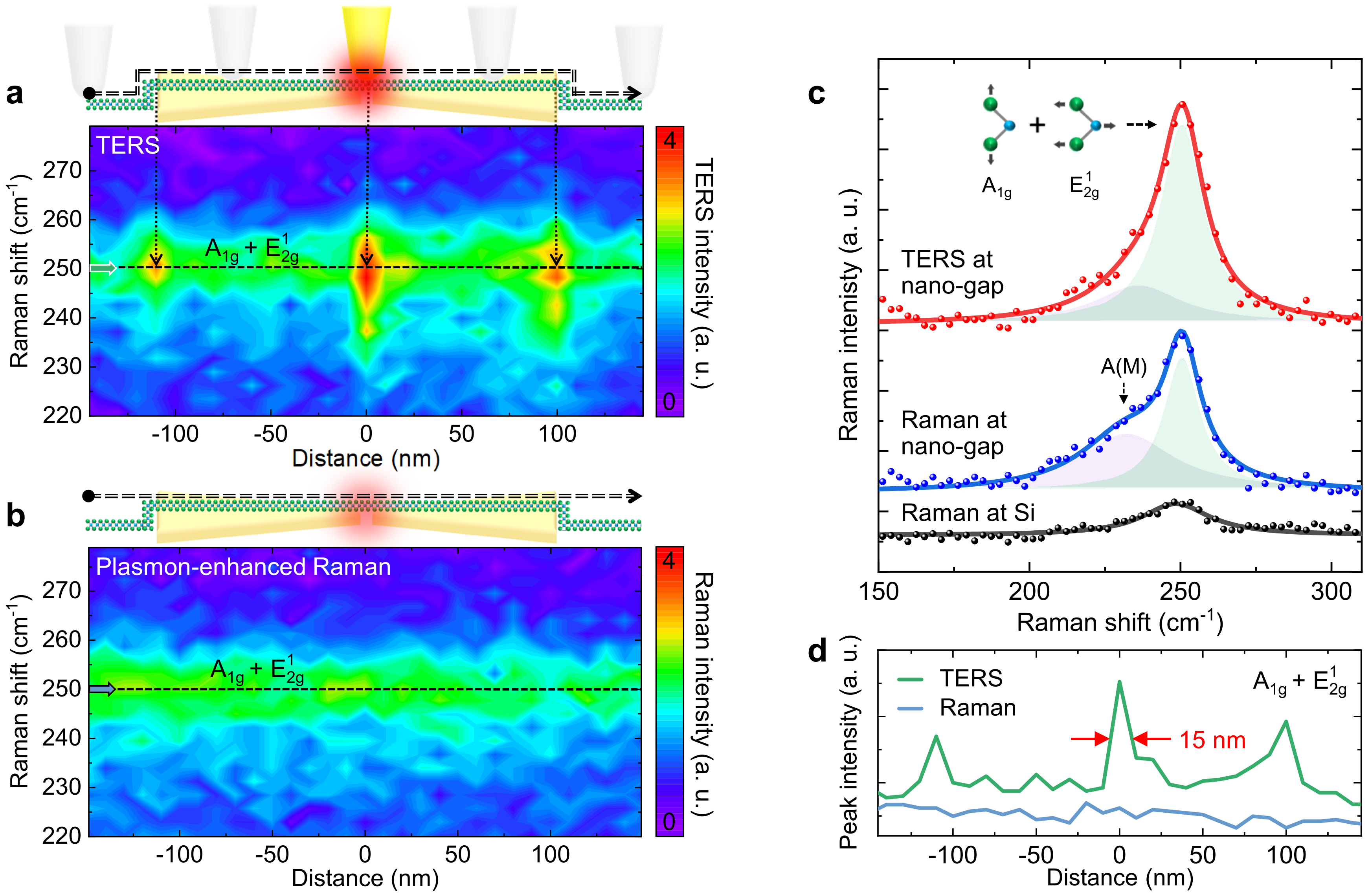
Figure 2a shows a spectral variation of tip-enhanced Raman spectroscopy (TERS) responses for a WSe2 ML when the Au tip moves along the longitudinal axis of the bowtie antenna. The distinct TERS response of the A1g + E mode (250 cm-1, degenerate mode for out-of-plane vibration of Se atoms and in-plane vibration of W and Se atoms [30, 31]) is observed in the nano-gap and both edges of the bowtie antenna. These three spots correspond to the slipping down regions of the transferred crystal.
In contrast, this spatial heterogeneity cannot be resolved in the plasmon-enhanced Raman profile (Figure 2b) due to the resolution limit. To understand the physical mechanism of the strong TERS response in the three local regions, we investigate spectral features by plotting TERS (red) and plasmon-enhanced Raman (blue) spectra in the nano-gap as shown in Figure 2c. While the A(M) mode (235 cm-1, asymmetric phonon mode at the M point [32, 33]) shows no distinct enhancement, the A1g + E mode shows significant signal enhancement in the TERS measurement. In the nano-gap, the vibration direction of the out-of-plane Raman mode (A1g) and in-plane Raman mode (E) are not matched with the polarization axis of the nano-gap plasmon in the bowtie antenna because of the rotated geometry of the 2D crystal caused by the dramatic sloping down structure. The strong enhancement of TERS intensity in the nano-gap well indicates the effect of the tip which enhances the z-polarized near-field dominantly. Therefore, we can assume that the E mode is the dominant vibrational mode in the TERS peak of the A1g E mode. i.e., the E mode is in parallel with respect to the tip-axis and the dominant near-field polarization [34, 35, 36]. Figure 2d shows TERS (green) and plasmon-enhanced Raman (blue) intensity profiles for the A1g E peak to quantify the spatial resolution of our approach, i.e., 15 nm.
2.3 Radiative emission of localized excitons at room temperature
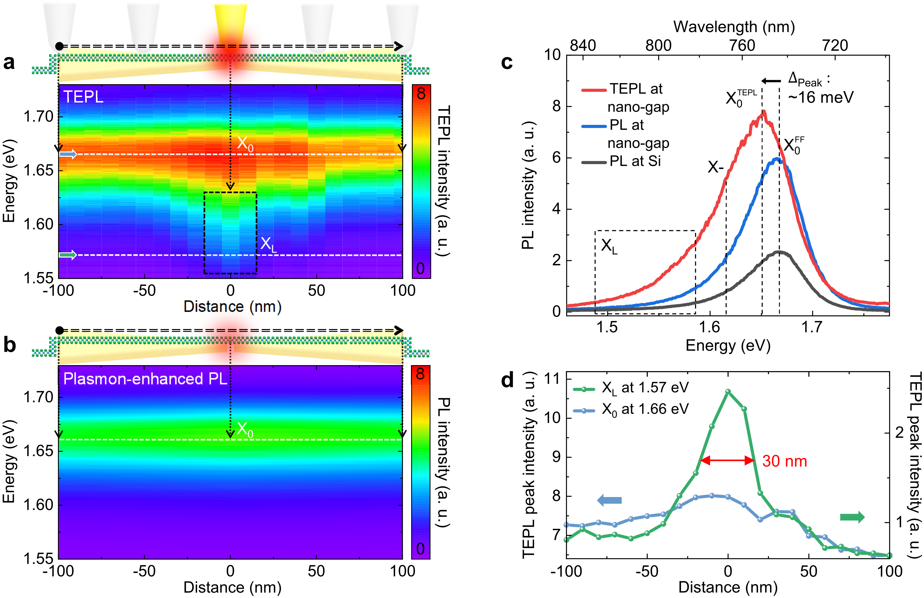
Figure 3a shows a variation of the TEPL spectra of the WSe2 ML when the Au tip moves along the longitudinal axis of the bowtie antenna. When the tip is located on the Au surface of the bowtie antenna, the TEPL signal of X0 is observed, yet with no PL response of XL. In contrast, the pronounced spectral change in TEPL signal is observed when the tip is located above the nano-gap. As indicated in Figure 3a (dashed box, XL), the additional lower-energy shoulder emerges near the nano-gap which corresponds to the radiative emission of XL.
On the other hand, the XL emission is not observed in the plasmon-enhanced far-field PL spectra (Figure 3b) due to the diffraction limited spatial resolution. To investigate the modified spectral feature with the triple-sharp-tips structure in detail, we compare the plasmon-enhanced far-field PL and TEPL spectra in the nano-gap (derived from Figure 3a-b), as shown in Figure 3c. As for the comparison with a far-field PL spectrum of a WSe2 ML on Si substrate (black), a significant PL enhancement of the X0 is observed with the bowtie antenna (blue) owing to the strong in-plane field localization in the nano-gap, yet with no modification of spectral shape. In contrast, the TEPL spectrum (red) shows a peak shift of neutral exciton (X0: from 1.667 eV to 1.651 eV), as well as new emerging shoulders of the localized excitons (XL at 1.580 eV) and the trions (X- at 1.637 eV). Note that we assign the X- peak from the energy difference of 30 meV compared to the PL energy of the X0, based on previous studies [37, 38, 39]. The observed spectral red-shift of 16 meV for the X0 peak is attributed to the applied tensile strain in the nano-gap and corresponds to 0.3 strain based on previous studies [40]. This spectral shift cannot be observed in the plasmon-enhanced PL (Figure 3b) due to the limited spatial resolution in far-field measurement.
To quantify the spatial extent of bound excitons in the strain induced region, we plot the TEPL intensity profiles for the X0 and XL peaks as shown in Figure 3d. In contrast to the gradual increase of the X0 peak near the nano-gap, the XL peak shows dramatic enhancement in the vicinity of the nano-gap with a narrow full-width at half-maximum (FWHM) of 30 nm. Although the strain is formed in the 5 nm gap of the bowtie antenna, the created XL are naturally diffused into the crystal face [41]. The observed length scale is in good agreement with the exciton diffusion length of a WSe2 ML at room temperature [41, 42]. Note that the observed spatial extent of 30 nm for the XL emission is not limited by spatial resolution of TEPL because we achieve a spatial resolution of 15 nm with the same tip for TERS imaging (Figure 2a and d).
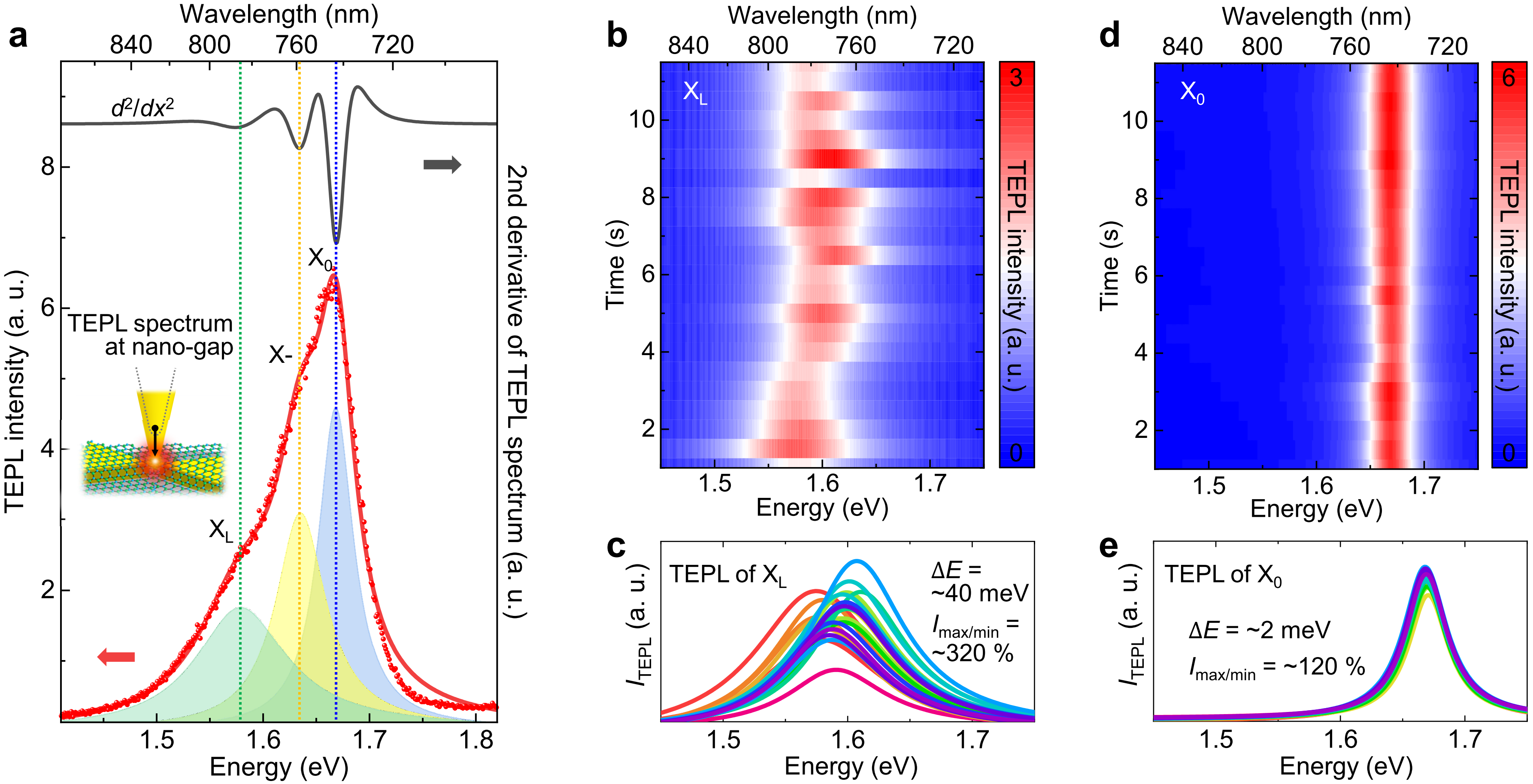
In the hyperspectral TEPL profiling (Figure 3a), the distance between the tip and sample is maintained at 3 nm with shear-force feedback. We then approach the Au tip further into the nano-gap to observe clearer TEPL spectrum from the triple-sharp-tips structure by increasing the field localization as well as the Purcell factor enhancement. Figure 4a shows the measured TEPL spectrum when the tip-sample distance is 1 nm. From fitting to the Voigt line shape function, we can derive distinct peaks of X0 (blue), X- (yellow), and XL (green) responses. In addition, we calculate the second derivative of the TEPL spectrum (black) to reconfirm the peak positions from them. As can be seen in Figure. 4a, the minimum points of the second derivative curve exactly correspond to X0, X-, and XL peaks. The reproducibility of our deterministic XL emission control is confirmed through the repeated experiments with different bowtie antennas (Figure S2 in Supporting Information)
We then measure the TEPL spectra as a function of time at the fixed tip-sample distance to investigate spectral fluctuation and blinking behavior of the XL PL. Figure 4b and d show TEPL evolutions of the XL and X0 peaks derived from Voigt fitting (Figure S3 in Supporting Information for details). While the X0 peaks show stable emission in intensity and energy, the XL peaks show distinct spectral and intensity fluctuations. All the emission spectra of XL and X0 over time are shown in Figure 4c and e to better visualize the spectral variation of the XL peaks. Peak energy shifts are observed as large as 40 meV for the XL peaks and 2 meV for the X0 peaks. In addition, the ratio of maximum and minimum peak intensities are 320 and 120 for the XL and X0 peaks. Furthermore, the XL emission shows a 2.5 broader PL linewidth compared to the X0 emission since different confinement potentials are formed across the strain-induced regions and the XL are trapped with having different energy states [12, 3, 27]. Therefore, the observed spectral fluctuations and broad linewidth of the XL show the typical characteristics of single quantum emitters [43, 44].
2.4 Electromagnetic simulations of the optical field and radiative decay rate
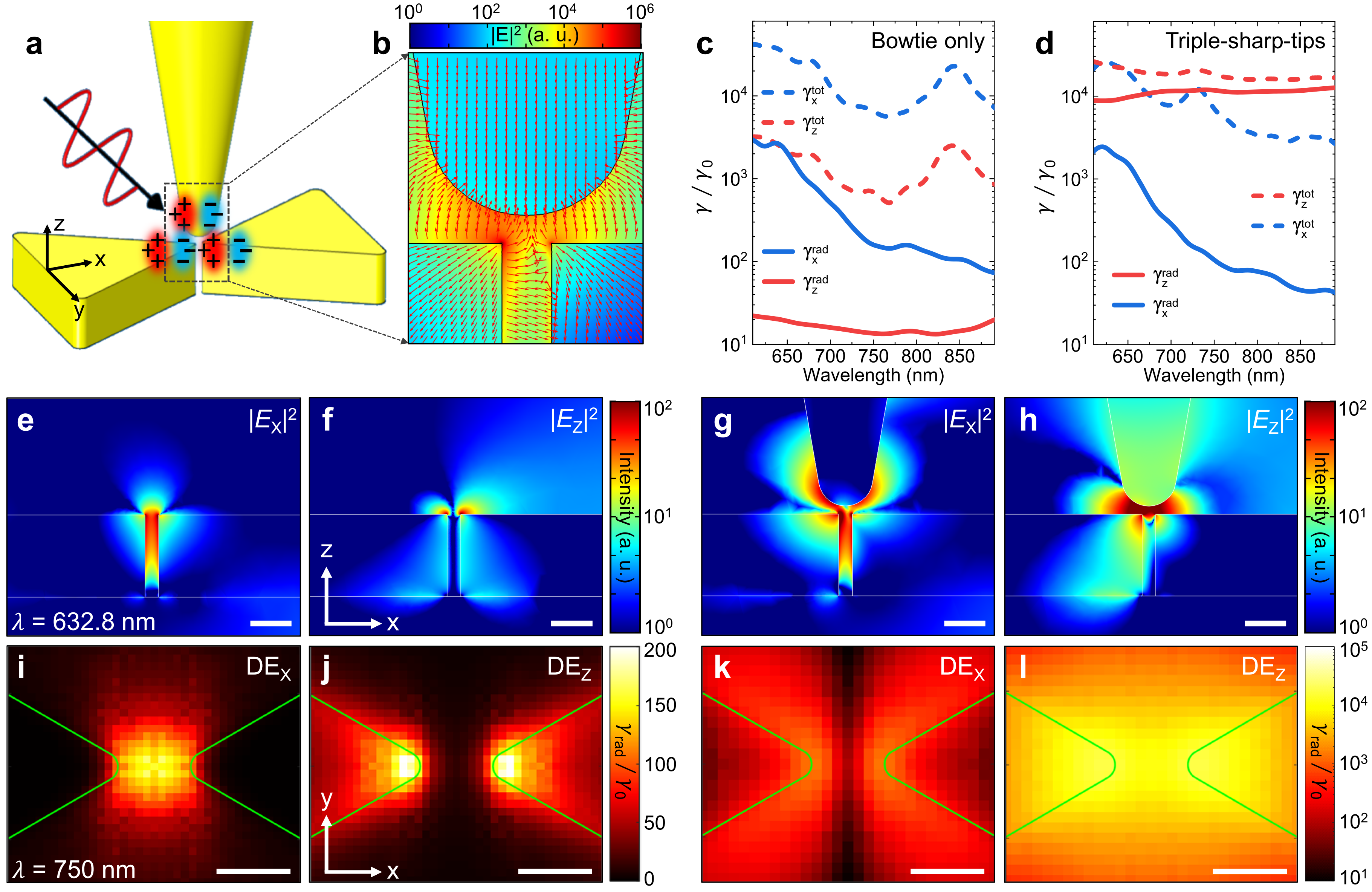
To quantitatively investigate the optical properties of the triple-sharp-tips cavity, we model it (Figure 5a) and perform numerical analysis using finite-element method (FEM) for the field distribution and finite-difference time-domain (FDTD) for local density of states (LDOS) calculation (see Experimental Section for details). When an excitation optical field (632.8 nm) is coupled to the cavity, electric charges of the Au nano-structures resonantly oscillate with the distribution illustrated in Figure 5a. Figure 5b shows the simulated optical field intensity distribution of the cavity with a vector-field map to understand the excitation rate enhancement. In the cavity, the excitation field intensity is enhanced as high as 106 with the dominant out-of-plane optical field in the nano-gap between the etched tip and bowtie tips.
We simulate the decay-rate enhancement of a spontaneous emitter placed in the cavity (1.5 nm above the top surface of the bowtie antenna) with respect to the emission wavelength. Figure 5c and d show the cross-sections of the total- (dashed) and radiative-decay-rate (solid) enhancement of the x- (blue) and z-axis (red) polarized dipole emitters for the bowtie only (c) and triple-sharp-tips (d) cavities. While the nonradiative-decay-rate ( - ) is quite large for both x- and z-polarized dipole emitters in the bowtie-only cavity (Figure 5c), the in the triple-sharp-tips cavity is significantly decreased for the z-polarized emitter in Figure 5d) due to Purcell effect in the confined cavity structure [29].
We then calculate the in-plane and out-of-plane optical field intensity distribution separately to compare the excitation rate for X0 () and XL () in the cavities, as shown in Figure 5e-h. When the Au tip is added to the bowtie antenna, at 1.5 nm above the bowtie nano-gap (Fig. 5g) shows comparable intensity with the bowtie-only antenna (Figure 5e). In contrast, is increased from 10 for the bowtie-only antenna to 102 for the triple-sharp-tips antenna by the added Au tip effect (Figure 5h) and we can estimate the excitation rate for XL in our experiment.
Next, to quantify the enhanced spontaneous emission rate from the Purcell effect in our TEPL measurements, we simulate the distribution of the radiative-decay-rate enhancement (/) for the x- and z-polarized dipole emitters (750 nm, 2D plane 1.5 nm above the top surface of the bowtie antenna) in both cavities, as shown in Figure 5i-l. Similar to the confirmed out-of-plane cavity effect on the excitation rate, we obtain as high as 104 for the z-polarized emitter in the triple-sharp-tips cavity (Figure 5l). These simulated excitation and emission rates for the z-polarized emitters in the cavity explain the room temperature observation of XL emission in our TEPL experiment. In general, XL PL is hard to observe at room temperature with far-field measurement because of the rapid decrease in quantum yield with increasing temperature caused by thermal activation of carriers and low exciton binding energy of XL [19, 17, 18]. On the other hand, the highly increased emission rate as well as the excitation field localization in the triple-sharp-tips cavity allows us to induce and probe XL TEPL in our experiment [14].
3 Discussions
Our experiment is carefully designed to induce, probe, and control the radiative emission of XL at room temperature. We fabricate extremely sharp bowtie tips [22] (RoC of 1 nm) and transfer a WSe2 monolayer on it. The monolayer crystal has a steep curve in the nano-gap which gives rise to an anisotropic tensile strain in the downward direction [45]. This local strain leads to induce XL with a vertically oriented transition dipole moment [43, 11, 46].
Although XL are created in this device, their radiative emission is not observed with far-field measurement. Since the orientation of the transition dipole moment of XL is perpendicular to the polarization of the nano-gap plasmon of the bowtie antenna, the XL cannot be effectively excited, radiatively emitted, and optically detected. Furthermore, the emission cannot be selectively and locally probed with far-field optics due to the diffraction limit. Hence, to locally probe the XL emission, we introduce an Au tip to form triple-sharp-tips structures (Figure 1a).
In this nano-cavity device, we can significantly increase the excitation rate ( 102) of the vertically oriented XL owing to the strong out-of-plane field localization (Figure 5h). In addition, the spontaneous emission rate is largely enhanced by the Purcell effect ( 104) because the mode volume in triple-sharp-tips cavity is extremely small (Figure 5l) compared to a conventional Au tip – metal mirror substrate platform [47, 29]. Based on our electromagnetic simulation results, we can estimate a TEPL enhancement factor of the localized excitons as high as 106 with an equation given by [29]
EF .
As a result, our triple-sharp-tips approach in combination with TEPL nano-spectroscopy enables us to induce and probe XL emission. Moreover, precise 3D tip positioning (0.2 nm) based on atomic force control provides the ability to dynamically engineer the cavity mode volume, field strength, and corresponding XL emission, as can be seen in the lateral (Figure 3a) and vertical (Figure 4a) tip-positioning effects. Therefore, our work demonstrates a systematic method to induce, probe, and control the single quantum emitters in atomically thin semiconductors even at room temperature.
4 Conclusion
In conclusion, we have demonstrated that ultracompact tip-enhanced nano-cavity spectroscopy with a triple-sharp-tips geometry gives access to localized states of excitons, beyond the limitations of previous XL studies, such as observation at cryogenic temperature, limited spatial resolution, or the lack of systematic control. Most importantly, the carefully designed cavity structure provides a Purcell factor as high as 104 for XL emitters with the ability to dynamically control the cavity mode volume (V) and corresponding radiative emission rate ( ) [48, 49, 50, 44]. We expect that this platform enabling bright XL emission and robust control at room temperature will allow a range of device applications for quantum information technology. The presented PL enhancement ( 106) method will be applied to greatly improve the efficiency and performance of quantum photonic devices [51, 52]. In addition, the previously demonstrated electrically-driven single quantum emission (electroluminescence) in 2D materials at cryogenic temperature [53, 54, 55, 14] can be realized in ambient condition by adopting our cavity structure. Furthermore, our tip-enhanced nano-cavity and -spectroscopy approach can be extended to characterize other low-dimensional quantum materials, such as zero-dimensional quantum dots [56, 57] and one-dimensional quantum wires [49], and induce and control their emitter-cavity interactions from the weak to the strong coupling regime [26].
5 Experimental Section
Sample preparation
To transfer the chemical vapor deposition (CVD)-grown WSe2 monolayer onto a flat Au film/coverslip, a wet transfer process was used.
As a first step, poly(methyl methacrylate) (PMMA) was spin-coated onto WSe2 monolayer grown on the SiO2 substrate.
The PMMA coated WSe2 monolayer was then separated from the SiO2 substrate using a hydrogen fluoride solution, and carefully transferred onto the bowtie device after being rinsed in distilled water to remove residual etchant.
Then, it is dried naturally for 6 hours to improve the adhesion.
Lastly, the PMMA was removed using acetone.
Bowtie fabrication
The sharp bowtie nanoantenna fabrication starts on a 500 m thick silicon substrate. Using standard electron beam lithography (Elionix ELS-7800, acceleration voltage 80 kV, beam current: 50 pA), the half bowtie patterns were defined on the copolymer (Microchem, MMA (8.5) MAA EL-8) / PMMA (Microchem, 495 PMMA A2) bilayer positive tone resist having different solubility in the developer. Such a bilayer process produces a T-shaped profile of the resist after development. The copolymer layer was spin-coated (5000 rpm, 60 seconds) and baked at 150∘C on the hotplate and its final thickness was about 250 nm. The PMMA layer was spin-coated (2000 rpm, 60 seconds) on the former copolymer layer and baked at 180∘C, its thickness was about 60 nm. After electron beam exposure, the copolymer / PMMA bilayer resist were developed in MIBK IPA 13 solutions for 23 minutes at 4∘C. A cold development with a longer develop time enables continuous development in the copolymer area affected by secondary electrons from the substrate while development in the PMMA layer is completed. As a result, a highly unstable T-shape resist profile can be made. The developed patterns were rinsed with IPA for 30 seconds and to dry out the remaining liquid, nitrogen gas was blown on the patterned area directly. The unstable resist patterns collapsed, and the collapsed pillars leaned on the adjacent wall where half bowtie patterns were inscribed. This kind of process, called cascade domino lithography, can realize ultra-sharp-edged photoresist masks with single digit nanometer scale gap size. The junctions between the rounded edge planes of the pillar and wall formed a sharp gap spacing resist mask. On the mask, Cr (3 nm) and Au (50 nm) were deposited by electron beam evaporation (KVT KVE-ENS4004), followed by the standard lift-off process. The fabricated bowtie antenna has a 1 nm-radius of curvature and 5 nm gap size, which cannot be realized by conventional electron beam lithography processes.
TERS/TEPL setup
The prepared WSe2 ML on bowtie antenna was loaded on a piezo-electric transducer (PZT, P-611.3x, Physik Instrumente) for XYZ scanning with 0.2 nm positioning precision. The Au tip (apex radius of 10 nm) fabricated with a refined electrochemical etching protocol was attached to a quartz tuning fork (resonance frequency of 32.768 kHz) to regulate the distance between the tip and sample under a shear-force AFM operated by a digital AFM controller (R9, RHK Technology). For TEPL and TERS experiment, a conventional optical spectroscopy set-up was combined with the home-built shear-force AFM. For a high quality wavefront of the excitation beam, a He-Ne laser (632.8 nm, 1 mW) was coupled and passed through a single-mode fiber (core diameter of 3.5 m) and collimated again using an aspheric lens. The collimated beam was then passed through a half-wave plate to make the excitation polarization parallel with respect to the tip axis. Finally, the beam was focused onto the Au tip using a microscope objective (NA0.8, LMPLFLN100, Olympus) with a side-illumination geometry. To ensure highly efficient laser coupling to the Au tip, the tip position was controlled with 30 nm precision by using Picomotor actuators (9062-XYZ-PPP-M, Newport). TEPL and TERS responses were collected using the same microscope objective (backscattering geometry) and passed through an edge filter (LP02-633RE-25, Semrock) to cutoff the fundamental line. The signals were then dispersed onto a spectrometer (f328 mm, Kymera 328i, Andor) and imaged with a thermoelectrically cooled charge-coupled device (CCD, iDus 420, Andor) to obtain TEPL and TERS spectra. Before the experiment, the spectrometer was calibrated with a Mercury lamp. A 150gmm grating with 800 nm blazed (spectral resolution of 0.62 nm) and 600gmm grating with 500 nm blazed (spectral resolution of 3.75 cm-1) were used for PL and Raman measurements, respectively.
Numerical analysis
Three dimensional full-wave simulations were performed to numerically analyze field enhancement and local density of states (LDOS) near the bowtie and the tip. Field enhancements (Figure 5b, e–h) were calculated using the Wave Optics module of COMSOL Multiphysics. A TM-polarized planewave incidence at 45∘ from air to a single bowtie with the tip was considered using the scattered field formulation surrounded by perfectly matched layer (or PML). LDOS (Figure 5c, d, i–l) were calculated using Lumerical FDTD. Total radiated power from an electric dipole and absorbed power to the total system were calculated to obtain the total and nonradiative decay rates [58]. Optical properties of silicon were taken from Palik [59], and gold from Johnson and Christy [60].
Supporting Information Supporting Information is available from the Wiley Online Library or from the author.
Acknowledgements This work was supported by the National Research Foundation of Korea (NRF) grants (No. 2019K2A9A1A06099937, and 2020R1C1C1011301). J.R. acknowledges the NRF grants (NRF-2019R1A2C3003129, CAMM-2019M3A6B3030637, NRF-2019R1A5A8080290, NRF-2018M3D1A1058998) funded by the Ministry of Science and ICT (MSIT). I.K. aknowledges the NRF Global Ph.D. fellowship (NRF-2016H1A2A1906519) funded by the Ministry of Education of the Korea govermnent. Y.K. acknowledges a fellowship from the Hyundai Motor Chung Mong-Koo Foundation. M.S.J. thanks the Creative Materials Discovery Program through NRF funded by the MSIT (NRF-2019M3D1A1078304). The authors thank D.S.L. and J.H.C. for the assistance of figure illustraion.
References
- [1] H. Lee, D. Y. Lee, M. G. Kang, Y. Koo, T. Kim, K.-D. Park, Nanophotonics 2020, 9, 10.
- [2] Y.-M. He, S. Höfling, C. Schneider, Opt. Express 2016, 24, 8 8066.
- [3] Y.-M. He, G. Clark, J. R. Schaibley, Y. He, M.-C. Chen, Y.-J. Wei, X. Ding, Q. Zhang, W. Yao, X. Xu, et al., Nat. Nanotechnol. 2015, 10, 6 497.
- [4] J. Dang, S. Sun, X. Xie, Y. Yu, K. Peng, C. Qian, S. Wu, F. Song, J. Yang, S. Xiao, et al., npj 2D Mater and Appl. 2020, 4, 1 1.
- [5] S. Zhang, C.-G. Wang, M.-Y. Li, D. Huang, L.-J. Li, W. Ji, S. Wu, Phys. Rev. Lett. 2017, 119, 4 046101.
- [6] A. Srivastava, M. Sidler, A. V. Allain, D. S. Lembke, A. Kis, A. Imamoğlu, Nat. Nanotechnol. 2015, 10, 6 491.
- [7] M. Koperski, K. Nogajewski, A. Arora, V. Cherkez, P. Mallet, J.-Y. Veuillen, J. Marcus, P. Kossacki, M. Potemski, Nat. Nanotechnol. 2015, 10, 6 503.
- [8] L.-M. Duan, M. D. Lukin, J. I. Cirac, P. Zoller, Nature 2001, 414, 6862 413.
- [9] Z. Ou, Phys. Rev. A 2008, 78, 2 023819.
- [10] M. Shahriar, P. Kumar, P. Hemmer, Journal Phys. B: At. Mol. Opt. 2012, 45, 12 124018.
- [11] O. Iff, N. Lundt, S. Betzold, L. N. Tripathi, M. Emmerling, S. Tongay, Y. J. Lee, S.-H. Kwon, S. Höfling, C. Schneider, Opt. Express 2018, 26, 20 25944.
- [12] A. Branny, S. Kumar, R. Proux, B. D. Gerardot, Nat. Commun. 2017, 8, 1 1.
- [13] E. Palacios, S. Park, S. Butun, L. Lauhon, K. Aydin, Appl. Phys. Lett. 2017, 111, 3 031101.
- [14] Y. Luo, G. D. Shepard, J. V. Ardelean, D. A. Rhodes, B. Kim, K. Barmak, J. C. Hone, S. Strauf, Nat. Nanotechnol. 2018, 13, 12 1137.
- [15] C. Chakraborty, A. Mukherjee, H. Moon, K. Konthasinghe, L. Qiu, W. Hou, T. Peña, C. Watson, S. M. Wu, D. Englund, et al., Optica 2020, 7, 6 580.
- [16] H. Kim, J. S. Moon, G. Noh, J. Lee, J.-H. Kim, Nano Lett. 2019, 19, 10 7534.
- [17] J. Huang, T. B. Hoang, M. H. Mikkelsen, Sci. Rep. 2016, 6 22414.
- [18] J. Pandey, A. Soni, Appl. Surf. Sci. 2019, 463 52.
- [19] J. S. Ross, S. Wu, H. Yu, N. J. Ghimire, A. M. Jones, G. Aivazian, J. Yan, D. G. Mandrus, D. Xiao, W. Yao, et al., Nature Commun. 2013, 4, 1 1.
- [20] Y. Lee, S. J. Yun, Y. Kim, M. S. Kim, G. H. Han, A. Sood, J. Kim, Nanoscale 2017, 9, 6 2272.
- [21] T. P. Darlington, C. Carmesin, M. Florian, E. Yanev, O. Ajayi, J. Ardelean, D. A. Rhodes, A. Ghiotto, A. Krayev, K. Watanabe, et al., Nat. Nanotechnol. 2020, 1–7.
- [22] I. Kim, J. Mun, K. M. Baek, M. Kim, C. Hao, C.-W. Qiu, Y. S. Jung, J. Rho, Mater. Today 2020.
- [23] E. M. Purcell, H. C. Torrey, R. V. Pound, Phys. Rev. 1946, 69, 1-2 37.
- [24] A. Martín-Jiménez, A. I. Fernández-Domínguez, K. Lauwaet, D. Granados, R. Miranda, F. J. García-Vidal, R. Otero, Nat. Commun. 2020, 11, 1 1.
- [25] G. M. Akselrod, C. Argyropoulos, T. B. Hoang, C. Ciracì, C. Fang, J. Huang, D. R. Smith, M. H. Mikkelsen, Nat. Photon. 2014, 8, 11 835.
- [26] K.-D. Park, M. A. May, H. Leng, J. Wang, J. A. Kropp, T. Gougousi, M. Pelton, M. B. Raschke, Sci. Adv. 2019, 5, 7 eaav5931.
- [27] T. Hidouri, F. Saidi, H. Maaref, P. Rodriguez, L. Auvray, Vacuum 2016, 132 10.
- [28] M. Feierabend, S. Brem, E. Malic, Phys. Chem. Chem. Phys. 2019, 21, 47 26077.
- [29] K.-D. Park, T. Jiang, G. Clark, X. Xu, M. B. Raschke, Nat. Nanotechnol. 2018, 13, 1 59.
- [30] H. Sahin, S. Tongay, S. Horzum, W. Fan, J. Zhou, J. Li, J. Wu, F. Peeters, Phys. Rev. B 2013, 87, 16 165409.
- [31] E. Del Corro, H. Terrones, A. Elias, C. Fantini, S. Feng, M. A. Nguyen, T. E. Mallouk, M. Terrones, M. A. Pimenta, ACS Nano 2014, 8, 9 9629.
- [32] H. Terrones, E. Del Corro, S. Feng, J. Poumirol, D. Rhodes, D. Smirnov, N. Pradhan, Z. Lin, M. Nguyen, A. Elias, et al., Sci. Rep. 2014, 4 4215.
- [33] X. Zhang, X.-F. Qiao, W. Shi, J.-B. Wu, D.-S. Jiang, P.-H. Tan, Chem. Soc. Rev. 2015, 44, 9 2757.
- [34] L. Tong, X. Duan, L. Song, T. Liu, L. Ye, X. Huang, P. Wang, Y. Sun, X. He, L. Zhang, et al., Appl. Mater. Today 2019, 15 203.
- [35] H. Zeng, G.-B. Liu, J. Dai, Y. Yan, B. Zhu, R. He, L. Xie, S. Xu, X. Chen, W. Yao, et al., Sci. Rep. 2013, 3 1608.
- [36] W. Zhao, Z. Ghorannevis, K. K. Amara, J. R. Pang, M. Toh, X. Zhang, C. Kloc, P. H. Tan, G. Eda, Nanoscale 2013, 5, 20 9677.
- [37] W. Bao, N. J. Borys, C. Ko, J. Suh, W. Fan, A. Thron, Y. Zhang, A. Buyanin, J. Zhang, S. Cabrini, et al., Nat. Commun. 2015, 6, 1 1.
- [38] A. M. Jones, H. Yu, N. J. Ghimire, S. Wu, G. Aivazian, J. S. Ross, B. Zhao, J. Yan, D. G. Mandrus, D. Xiao, et al., Nat. Nanotechnol. 2013, 8, 9 634.
- [39] Y. You, X.-X. Zhang, T. C. Berkelbach, M. S. Hybertsen, D. R. Reichman, T. F. Heinz, Nat. Phys. 2015, 11, 6 477.
- [40] R. Schmidt, I. Niehues, R. Schneider, M. Drueppel, T. Deilmann, M. Rohlfing, S. M. De Vasconcellos, A. Castellanos-Gomez, R. Bratschitsch, 2D Mater. 2016, 3, 2 021011.
- [41] K.-D. Park, O. Khatib, V. Kravtsov, G. Clark, X. Xu, M. B. Raschke, Nano Lett. 2016, 16, 4 2621.
- [42] A. M. Van Der Zande, P. Y. Huang, D. A. Chenet, T. C. Berkelbach, Y. You, G.-H. Lee, T. F. Heinz, D. R. Reichman, D. A. Muller, J. C. Hone, Nat. Mater. 2013, 12, 6 554.
- [43] P. Tonndorf, R. Schmidt, R. Schneider, J. Kern, M. Buscema, G. A. Steele, A. Castellanos-Gomez, H. S. van der Zant, S. M. de Vasconcellos, R. Bratschitsch, Optica 2015, 2, 4 347.
- [44] Y. Luo, N. Liu, X. Li, J. C. Hone, S. Strauf, 2D Mater. 2019, 6, 3 035017.
- [45] M. Cotrufo, L. Sun, J. Choi, A. Alù, X. Li, Nanophotonics 2019, 8, 4 577.
- [46] A. Lundskog, C.-W. Hsu, K. F. Karlsson, S. Amloy, D. Nilsson, U. Forsberg, P. O. Holtz, E. Janzén, Light: Sci. & Appl. 2014, 3, 1 e139.
- [47] M.-E. Kleemann, R. Chikkaraddy, E. M. Alexeev, D. Kos, C. Carnegie, W. Deacon, A. C. De Pury, C. Große, B. De Nijs, J. Mertens, et al., Nat. Commun. 2017, 8, 1 1.
- [48] J. A. Schuller, S. Karaveli, T. Schiros, K. He, S. Yang, I. Kymissis, J. Shan, R. Zia, Nat. Nanotechnol. 2013, 8, 4 271.
- [49] Y. Luo, E. D. Ahmadi, K. Shayan, Y. Ma, K. S. Mistry, C. Zhang, J. Hone, J. L. Blackburn, S. Strauf, Nat. Commun. 2017, 8, 1 1.
- [50] M. Pelton, Nat. Photon. 2015, 9, 7 427.
- [51] V. Zwiller, T. Aichele, O. Benson, New J. Phys. 2004, 6, 1 96.
- [52] A. Schlehahn, A. Thoma, P. Munnelly, M. Kamp, S. Höfling, T. Heindel, C. Schneider, S. Reitzenstein, APL Photonics 2016, 1, 1 011301.
- [53] J. S. Ross, P. Klement, A. M. Jones, N. J. Ghimire, J. Yan, D. Mandrus, T. Taniguchi, K. Watanabe, K. Kitamura, W. Yao, et al., Nat. Nanotechnol. 2014, 9, 4 268.
- [54] B. W. Baugher, H. O. Churchill, Y. Yang, P. Jarillo-Herrero, Nat. Nanotechnol. 2014, 9, 4 262.
- [55] A. Pospischil, M. M. Furchi, T. Mueller, Nat. Nanotechnol. 2014, 9, 4 257.
- [56] K. J. Vahala, Nature 2003, 424, 6950 839.
- [57] Ł. Dusanowski, D. Köck, E. Shin, S.-H. Kwon, C. Schneider, S. Höfling, Nano Lett. 2020.
- [58] D. L. Mack, E. Cortés, V. Giannini, P. Török, T. Roschuk, S. A. Maier, Nat. Commun. 2017, 8, 1 1.
- [59] D. P. Edward, I. Palik, Handbook of optical constants of solids, 1985.
- [60] P. B. Johnson, R.-W. Christy, Phys. Rev. B 1972, 6, 12 4370.