Electronic correlation, magnetic structure and magnetotransport in few-layer CrI3
Abstract
Using density functional theory combined with a Hubbard model (DFT+U), the electronic band structure of CrI3 multilayers, both free-standing and enclosed between graphene contacts, is calculated. We show that the DFT+U approach, together with the ‘around mean field’ correction scheme, is able to describe the vertical magnetotransport in line with the experimental measurements of magnetoresistance in multi-layered CrI3 enclosed between graphene contacts. Moreover, by interpolating between different double-counting correction schemes, namely the ‘around mean field’ correction and the fully localized limit, we show their importance for describing both the band structure and the ground-state total energy consistently. Our description of the magnetic exchange interaction is compatible with the experimentally observed antiferromagnetic ground state in the bilayer CrI3 and the transition to a ferromagnetic arrangement in a small external magnetic field. Thus, using spin-polarized DFT+U with an ‘around mean field’ correction, a consistent overall picture is achieved.
I Introduction
Experimental realization of magnetism in two-dimensional (2D) atomic crystals has attracted the attention of many researchers Gibertini et al. (2019), in particular because of its promising applications in spintronics. However, our basic understanding of these materials is still far from complete and poses many challenges to predictive electronic structure theory. Potential pitfalls and remedies will be exemplified by the present study of CrI3 using density functional theory (DFT). Researchers were puzzled by the observation that CrI3 is ferromagnetic (FM) as bulk materialTsubokawa (1960); Dillon and Olsen (1965), while stacks of few atomic layers of CrI3 show antiferromagnetic (AFM) interlayer exchange Huang et al. (2017). Electronic structure calculations with local or semi-local density functionals reproduced the ferromagnetism of bulk and single-layer CrI3 Wang et al. (2011); Sivadas et al. (2018); Lado and Fernández-Rossier (2017); Jiang et al. (2018a); Zheng et al. (2018), but failed to describe the antiferromagnetic coupling in bilayers Jang et al. (2019). This discrepancy could be attributed to the structural anomalies Thiel et al. (2019); Ubrig et al. (2019) in thin films or to an insufficient description of their electronic structure by standard computational methods. Obviously, knowledge of the exact energetic position of the Cr orbitals and their contribution to the electronic band structure play a crucial role for resolving this issue. We show that an informed description of the electronic correlation at the Cr atoms using the DFT+U approach not only reconciles the different magnetic properties of bulk and thin layers of CrI3, but is also mandatory for understanding magnetotransport effects observed in layered structures Klein et al. (2018); Wang et al. (2018). By carefully selecting the appropriate theoretical tools and comparing their implications to available experimental data, we demonstrate that it is possible to assign a meaningful value to the Hubbard parameter U and to analyze electronic, magnetic and transport properties of this complex material in a common theoretical perspective.
In this paper, we briefly review the methodology of DFT+U calculations and discuss the band structure of bilayer CrI3 for two alternative schemes of the double-counting correction. We will argue that the ‘around-mean-field’ correction scheme gives results consistent with experiment, and corroborate this claim by presenting computational results for the magnetic structure of bi- layer and trilayer CrI3. Finally, magnetotransport perpendicular to CrI3 thin films between graphene contacts will be discussed on the basis of calculated band structures in conjunction with a model Hamiltonian.
II Methodology
As starting point of our theoretical investigation, we briefly summarize the basic knowledge of the atomic and electronic structure of CrI3. In its bulk form, CrI3 is a layered compound with a high-temperature (HT) and a low-temperature (LT) phase that differ in the relative spatial arrangement of the stacked layer bundles (see section S2 in the supplementary material). Each layer bundle consists of a central layer of Cr atoms forming a honeycomb lattice, sandwiched between two iodine layers. The Cr atom (valence configuration ) is trivalent in CrI3 and gives away three of its six valence electrons to the monovalent iodine atoms. The remaining three electrons are spin-polarized and occupy orbitals of the majority spin channel, giving rise to a magnetic moment of per formula unit. The conduction band in the majority spin channel is formed by the unoccupied orbitals. In the minority spin channel, all five orbitals of Cr are unoccupied and hybridize to form the conduction bands of minority spin. These qualitative features of the electronic structure of CrI3 are already well reproduced in calculations with local or semi-local DFT functionals. However, a quantitative description of the materials properties relies on knowledge of the precise energetic position of the Cr-derived bands. In particular, the size of the band gap in the majority spin channel has an important effect on the magnitude of the exchange interaction, as will be outlined below. Such an improved description can be achieved by the DFT+U method Anisimov et al. (1991); Dudarev et al. (1998) with a suitably chosen value of the Hubbard parameter that describes the screened on-site Coulomb repulsion of the Cr electrons. This can be seen as part of a more general effort to enhance DFT calculations by a quantum many-body Hamiltonian that may contain the interatomic Hund exchange as well as the Stoner parameter as further parameters in addition to . While the capabilities of model Hamiltonians have been explored e.g. in Ref. Ryee and Han, 2018, here we concentrate solely on the effect of . Note that, even within a material of given chemical composition, the value of may vary for samples of different dimensionality, e.g. bulk or atomically thin films, due to variations of the electrostatic screening of the Coulomb interaction by the environment Rösner et al. (2016). Moreover, it is well known that calculations with the DFT+U scheme require a double-counting (DC) correction, i.e., the Coulomb repulsion of electrons already included in the DFT description must not be counted twice when adding the DFT+U correction term, see e.g. Ref. Park et al., 2014 for an in-depth discussion. Previous calculations Sivadas et al. (2018); Lado and Fernández-Rossier (2017); Jiang et al. (2018a); Zheng et al. (2018); Jang et al. (2019) of CrI3 tacitly relied on the fully localized limit (FLL) for this DC correction, a scheme based on the consideration that each sublevel of the Cr shell with magnetic quantum number is either fully occupied or empty. However, as we will discuss below, the description of the electronic structure by the FLL scheme may not be fully satisfactory, in particular when magnetotransport should be addressed.
Alternatively, we employ the ‘around mean field’ (AMF) scheme Czyżyk and Sawatzky (1994) that becomes exact if the sublevels are all equally occupied with an average occupation compatible with the spin density (per atom) suggested by the DFT treatment. Here, the exchange-correlation potential of DFT is considered as an effective mean field, thus motivating the name ‘around mean field’ correction. A more detailed derivation of the two approaches can be found in section S1 in the supplementary material. The shift of the Cr-derived energy bands introduced by the DC correction is reflected in the formulasPetukhov et al. (2003)
| (1) | |||||
| (2) |
The term stands for the density matrix of each spin channel (indexed by ) that is determined self-consistently during the DFT+U calculation. The indices refer to the magnetic quantum number within the 3d shell of Cr. In a diagonal representation, the diagonal elements of the density matrix, i.e. , have the meaning of occupation numbers. Consequently, the level shifts introduced by the may be positive or negative, depending on the average occupation of the levels. In the AMF scheme, the spin-dependent occupation originating from the DFT calculation serves as reference point. We note that energy correction terms for both types of can be constructed (see Supplemental Material); and thus it is possible to calculate not only the band structure, but also the total energy in both approaches.
We perform spin-polarized DFT calculations using the full-potential all-electron code FHI-aimsBlum et al. (2009) with a highly accurate basis set constructed from atom-centered numerical orbitals. For the exchange-correlation functional of DFT, we employ the generalized-gradient approximation (GGA) augmented with the Tkatchenko-Scheffler Tkatchenko and Scheffler (2009) pairwise dispersive correction in order to account for the dispersive interaction. Spin-orbit interactions was taken into account where indicated, using the method of second-order variations, as described in Ref. Huhn and Blum, 2017. A and Monkhorst-Pack Monkhorst and Pack (1976); Kratzer and Neugebauer (2019) k-point mesh was used for Brillouin zone integration for the bulk and slab geometry, respectively. For the two-dimensional geometries a vacuum of length 20 Å was considered along the normal direction. The geometrical optimization calculations for each scheme, AMF or FLL, were carried out until all the components of force on any atom is less than 5 meV/Å. We employ the isotropic variant of DFT+U Dudarev et al. (1998) treating as a single parameter. Treating the Hund exchange coupling as an independent parameters would offer an alternative approach to describe the electronic structure of CrI3 that has been attempted by others Subhan et al. (2019) recently. In addition to varying , we employ the linear interpolation scheme (see section S1 in the supplementary material) introduced by Petukhov et al.Petukhov et al. (2003) with an additional parameter allowing them to switch smoothly between the limiting cases of AMF ( and FLL . Variations of the Cr–I bond length with the value of and with the double-counting correction scheme were found to be negligibly small, in accord with previous studies Wang et al. (2011).
III Results
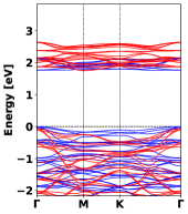
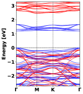
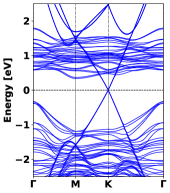
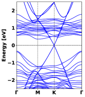
Electronic band structure Typical results for the band structure in the two limiting cases of the AMF or FLL correction are shown in Fig. 1. Our particular interest is in the position of the conduction bands depending on the type of approximation used. As a feature of the AMF scheme essential to the present study, we observe a large up-shift of the majority bands (Fig. 1a) compared to their position in pure DFT, while the up-shift of the unoccupied minority bands is still moderate. As a consequence, both spin channels lie in an overlapping energy range. In contrast, the FLL scheme with any reasonably large parameter results in a very large up-shift of the minority bands, whereas the band gap in the majority spin channel remains small (Fig. 1b). We will see below that the smaller gap in the FLL compared to the AMF scheme is closely related to preferred ferromagnetic ordering in the bilayer, whereas experiments rather point to a subtle energy balance between FM and AFM structures. The origin and sign of the shifts can be understood from the expressions in Eq.s (1) and (2): In the FLL scheme, the ‘neutral point’ where shifts change sign is located at half-filling of a sublevel, as can be seen from the 1/2 in second term in the parentheses in Eq. (2). In the present case of CrI3, it is mandatory to determine the ‘neural point’ independently for each spin channel, thereby preserving the magnetic moment of 3 per formula unit. With this prerequisite, the AMF correction turns out to be the better choice, as will be corroborated by the results presented below.
Magnetic properties CrI3 is a magnetic semiconductor with a gap of 1.2 eV Dillon and Olsen (1965) in bulk and sizable intra-layer coupling of the Cr magnetic moments within one layer, but weaker couplings between adjacent layers. The latter may depend on stacking and thus differ in the LT and HT phase Jang et al. (2019); Sivadas et al. (2018). The experimental observation that the magnetization in thin CrI3 layers can be switched by an external magnetic Huang et al. (2017); Thiel et al. (2019) or even an electric field Huang et al. (2018); Jiang et al. (2018b) points to a subtle balance between AFM and FM couplings in this material. For the intra-layer couplings, it has been suggested recently that there are two kinds of orbital-specific exchange interactions Kashin et al. (2020), an AFM interaction between occupied orbitals at different Cr atoms, and an FM interaction between an occupied orbital at one Cr and an unoccupied orbital at another Cr atom. We propose that this picture extends to the interlayer interactions. Applying arguments from second-order perturbation theory, it has been shown that the magnitude of the interactions is governed by the energetic distance (see Eq. 7 in Ref. Kashin et al., 2020) between these two orbital groups, and thus on the energetic position of the -type conduction bands in the majority spin. A high-lying band, as in Fig.1(a) using AMF DC correction, therefore reduces the strength of the FM interaction, whereas this interaction gets enhanced in case of a low-lying conduction band, as in Fig.1(b) using FLL. Thus it becomes clear that the experimentally observed AFM ground state of few-layer CrI3 can be reproduced only by methods that correctly account for the energetic up-shift of the unoccupied majority spin levels.
To provide evidence for this relation, we calculate the energy difference between FM and AFM interlayer magnetic arrangements as a function of two free parameters, and the interpolation parameter controlling the type of DC correction. Fig. 2 shows contour plots of this energy difference on a 2D grid of parameter values, covering values in a physical reasonable range, between 0.7 eV and 2.5 eV. This range is in agreement with previous studies: The constrained random-phase approximation method obtained eV for monolayer CrI3 and eV Jang et al. (2019). A positive (negative) value of the energy difference indicates an AFM (FM) interlayer magnetic arrangement has lower total energy. Next, we discuss and compare the results for bulk and for few-layer structures. In bulk CrI3, FM interlayer magnetic interaction is found to be favored for almost all choices of and , see Fig. 2(a). Only at high values of ( eV), and close to the AMF limit, i.e., , the energy difference approaches zero. Our results for the HT phase (not shown) of bulk CrI3 are very similar to the LT phase: With the AMF correction scheme we predict FM magnetic arrangement to be stable independent of the value of in the considered range.
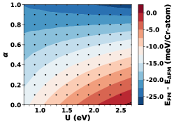
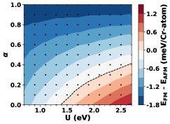
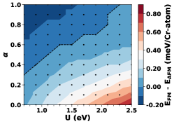
In the bilayer form of CrI3, both in LT and HT phase, our calculations show a cross-over from FM to AFM magnetic arrangement as is increased. The LT structure of bulk CrI3 would only become AFM at unrealistically high values of eV. For LT bilayer and trilayer (shown in the Fig. S1 in the supplementary material) CrI3, however, an AFM ground state is predicted for eV and small . In the AMF limit (), we can describe the magnetic exchange energy per Cr atom by an empirical relationship for the bilayer and for the trilayer.
Since is found to depend sensitively on , experimental information about the magnetic switching behavior can be used to determine the physically meaningful value of for a particular structure. In the remainder of this paper, we will argue that GGA+U with a value of eV, together with AMF DC correction, gives the best description of the electronic structure in few-layer structures that is in line with all experimental findings. The choice of eV for bilayers and trilayers is motivated by the experimentally observed magnetic field of 0.9 T required to induce the first transition of the magnetic structure when increasing the -fieldKlein et al. (2018). The Zeeman energy of 0.32 meV for flipping a magnetic moment of in this field equals the exchange energy obtained at eV in our calculation for the LT bilayer (Fig. 2(b)). The second magnetic transition was experimentally observed at a field about twice as large, B=1.8 TKlein et al. (2018). This is compatible with the idea that the AFM interlayer exchange interactions both to the layer above and below the central layer(s) must be overcome to induce switching in thicker samples. Different interpretations of magnetic switching, for instance a relation with a possible structural change from the HT to the LT phase, as has been suggested by experimental work Thiel et al. (2019); Ubrig et al. (2019), are also compatible with our calculations: The CrI3 bilayer in the HT phase is predicted to be AFM in the AMF correction scheme at any reasonable value (cf. Fig. 2(c)), and could thus serve as starting point at for the magnetic transitions observed. If one assumed the HT structure, one would arrive at a slightly smaller value of eV at which the Zeeman energy of 0.32 meV matches the exchange energy . However, the HT phase is 1.38 meV per Cr atom higher in energy than the LT phase according to our calculations (with eV and ), and we therefore prefer to continue the discussion under the assumption of the LT phase being present. Elaborating further on the relation between dimensionality and , we note that a low value (e.g. eV as suggested in Ref. Jang et al., 2019) may also be more appropriate inside bulk CrI3 due to enhanced dielectric screening. This would not affect our claim that the GGA+U scheme with AMF correction correctly captures the difference in magnetic properties of bulk and thin films, since this scheme predicts the interlayer exchange interaction in bulk to be FM over a wide range of values both in the LT (Fig. 2(a)) and the HT phase.
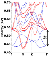
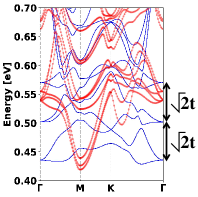
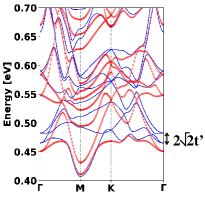
Magnetotransport Tunneling magnetotransport perpendicular to the layers has been measured both in atomically thin samples Klein et al. (2018) and in samples several tens of nanometers thick Wang et al. (2018), using graphene as contact material. In both studies, the tunneling current originated from electrons, rather than hole carriers. It was observed that the tunneling resistance is significantly lowered when the magnetization in the layers is aligned by an external magnetic field; this lowering amounts to a factor of 2, 4 and 6.5 in samples of 2, 3, and 4 layers (corresponding to magnetoresistance ratios of 100%, 300% and 550%, see Ref. Klein et al., 2018). Even larger magnetoresistance ratios, up to 8000%, were observed in thicker samplesWang et al. (2018). It is noteworthy that the magnetic fields at which the reduction of the resistance occurs are very similar, 0.9 T and 1.8 T in both types of samples, pointing to a common microscopic mechanism. In the following, we will argue that these findings are compatible with majority and minority conduction bands at about the same energy, as found in our GGA+U calculation with AMF correction, but cannot be reconciled with vastly different band energies, as typical for the FLL correction scheme.
A qualitative explanation of the magnetoresistance effect can be given already from a schematic energy level diagram as illustrated in Fig. 4. The van der Waals gap between CrI3 layers constitutes a barrier that must be overcome by the tunneling electrons. In an FM sample, the electrons will experience a periodic potential along the direction normal to the layers, with a period given by the layer thickness. The spin channel responsible for the conduction band minimum at the point formed by the orbitals with symmetry will contribute dominantly to the tunneling current. This is different from the situation of antiparallel magnetization between adjacent layers: In the limit of the number of layers being large, electrons of either spin will contribute equally to the tunneling current, since spin majority electrons in one layer are minority electrons in the next layer, and vice versa; thus both electron spin states are equivalent. However, despite the two channels contributing, the overall current will be lower than in the ferromagnetic case because the tunneling barriers are higher.

For a more quantitative analysis, we have worked out a toy model in form of a tight-binding Hamiltonian (see section S4 in the supplementary material) with two hopping amplitudes and for parallel and antiparallel layer magnetization, respectively. It is even possible to obtain estimates for these parameters from the GGA+U band structures. Comparing level splittings obtained from the eigenvalues of the tight-binding Hamiltonian with the calculated band structures in Fig. 3(a) and 3(b) yields meV as best estimate. In a similar way, the value meV can be derived by comparing the analytically obtained eigenvalues with the calculated band structure in Fig. 3(c).
According to the Landauer-Büttiker approach Datta (2005) to transport, the conductance is with the transmission probability or for parallel or antiparallel magnetization of the layers, respectively. The latter two quantities can be expressed in terms of the Green function of the tunneling electrons, and is hence related to the hopping amplitudes and in the Hamiltonian (see section S4 in the supplementary material for details). The transmission probability through a van-der-Waals gap between two layers with parallel spin alignment can be shown to be . For a ferromagnetic stack of layers, this expression generalizes to . For a stack with alternating spin orientation, tunneling through two subsequent van der Waals gaps yield a probability . For layers ( odd), the total probability is thus . For a spin-filter model similar to the one considered in Ref. Klein et al., 2018 the magnetoresistance ratio is given as
where the factor 2 stems from both spin channels contributing to transport in the antiparallel case. By inserting the values of meV and meV from our band structure calculations, we obtain ratios of 35 and 2400 for bi- and trilayers, respectively. We note that a modest increase of the magnetoresistance ratio with the number of layers, as observed in the experiment Klein et al. (2018), can be obtained only if and are of comparable magnitude, which in turn implies that the potentials experienced by spin-up and spin-down conduction electrons must be rather similar. For the AMF correction (see e.g. Fig. 1(a)) we are close to achieving this condition by fine-tuning around eV, while this goal is out of reach in calculations with the FLL correction (Fig. 1(b)), lending additional support to the AMF correction being the appropriate scheme for CrI3.
Eventually, we analyze the role of the graphene contacts. Clearly, the electrons need to tunnel from the graphene into the first layer of CrI3, and likewise tunnel out of the terminating CrI3 layer into the graphene at the other contact. Our GGA+U calculations including graphene top and bottom contacts show that the structure of the valence and conduction bands in CrI3 is essentially the same as in the free-standing bilayer. The weak van-der Waals interaction has a minor effect on the band structure, mostly mediated by the in-plane lattice constants which we assume to adjust to obtain a commensurate superstructure. The Dirac point of graphene, and thus the Fermi energy of (undoped) graphene, falls into the band gap of CrI3. Without applied voltage, the off-set between the conduction band edge and amounts to 0.42 eV at the M point and 0.44 eV at the -point (formed by orbitals of Cr). Under operating conditions, the potential drop between the graphene injector and the CrI3 central layers will pull the CrI3 conduction band minima closer to the Fermi energy in graphene. Our value for the off-set, being an upper bound for the injection barrier, is thus compatible with the activation energy of 0.15 eV found in temperature-dependent measurements of the magnetotransport Wang et al. (2018).
When analyzing the magnetoresistance ratio of multilayer samples between graphene contacts, one should take into consideration that at least the outermost layer, but possibly even two or three subsurface layers of CrI3, display magnetic ordering different from bulk. This is supported by experiments Wang et al. (2018) that report switching of the magnetic structure by applied magnetic fields similar to those in the few-layer samples. From the perspective of our GGA+U method with AMF correction, one is tempted to assume that some critical value of may exist for Cr atoms in a surface layer, in analogy to the transition for bilayer CrI3 observed in Fig. 2(b). If the critical value is exceeded, the interlayer coupling will turn AFM. It is plausible that Cr atoms in a surface layer should be described by a quite large , in between the values for bulk and bilayer, since dielectric screening is reduced near a surface or interface. Since this effect is to be expected both near the upper and lower interface of the sample with the graphene contacts, it could also help to explain the very large values of the magnetoresistance ratio observed in the thicker samples Wang et al. (2018).
IV Conclusions
In conclusion, we have demonstrated that the GGA+U approach to electronic structure, when applied in conjunction with double-counting corrections of ‘around mean field’ type, gives a consistent overall picture of the electronic structure of CrI3, its magnetic and transport properties. This approach carries over to other chromium trihalides; moreover, we believe that a fresh look at double counting correction schemes other than the commonly used ‘fully localized limit’ is in place when extending the GGA+U approach beyond transition metal oxides. This finding may have important consequences for calculations aiming at the prediction of magnetic exchange parameters and of magnetic ordering temperatures.
V Acknowledgments
The authors gratefully acknowledge the funding of this project by computing time provided by the Paderborn Center for Parallel Computing (PC2).
References
- Gibertini et al. (2019) M. Gibertini, M. Koperski, A. F. Morpurgo, and K. S. Novoselov, Nat. Nanotechnol. 14, 408 (2019).
- Tsubokawa (1960) I. Tsubokawa, J. Phys. Soc. Jpn. 15, 1664 (1960).
- Dillon and Olsen (1965) J. F. Dillon and C. E. Olsen, J. Appl. Phys. 36, 1259 (1965).
- Huang et al. (2017) B. Huang, G. Clark, E. Navarro-Moratalla, D. R. Klein, R. Cheng, K. L. Seyler, D. Zhong, E. Schmidgall, M. A. McGuire, D. H. Cobden, W. Yao, D. Xiao, P. Jarillo-Herrero, and X. Xu, Nature 546, 270 (2017).
- Wang et al. (2011) H. Wang, V. Eyert, and U. Schwingenschlögl, J. Phys.: Condens. Matter 23, 116003 (2011).
- Sivadas et al. (2018) N. Sivadas, S. Okamoto, X. Xu, C. J. Fennie, and D. Xiao, Nano Lett. 18, 7658 (2018).
- Lado and Fernández-Rossier (2017) J. L. Lado and J. Fernández-Rossier, 2D Mater. 4, 035002 (2017).
- Jiang et al. (2018a) P. Jiang, L. Li, Z. Liao, Y. X. Zhao, and Z. Zhong, Nano Lett. 18, 3844 (2018a).
- Zheng et al. (2018) F. Zheng, J. Zhao, Z. Liu, M. Li, M. Zhou, S. Zhang, and P. Zhang, Nanoscale 10, 14298 (2018).
- Jang et al. (2019) S. W. Jang, M. Y. Jeong, H. Yoon, S. Ryee, and M. J. Han, Phys. Rev. Materials 3, 031001 (2019).
- Thiel et al. (2019) L. Thiel, Z. Wang, M. A. Tschudin, D. Rohner, I. Gutiérrez-Lezama, N. Ubrig, M. Gibertini, E. Giannini, A. F. Morpurgo, and P. Maletinsky, Science 364, 973 (2019).
- Ubrig et al. (2019) N. Ubrig, Z. Wang, J. Teyssier, T. Taniguchi, K. Watanabe, E. Giannini, A. F. Morpurgo, and M. Gibertini, 2D Materials 7, 015007 (2019).
- Klein et al. (2018) D. R. Klein, D. MacNeill, J. L. Lado, D. Soriano, E. Navarro-Moratalla, K. Watanabe, T. Taniguchi, S. Manni, P. Canfield, J. Fernández-Rossier, and P. Jarillo-Herrero, Science 360, 1218 (2018).
- Wang et al. (2018) Z. Wang, I. Gutiérrez-Lezama, N. Ubrig, M. Kroner, M. Gibertini, T. Taniguchi, K. Watanabe, A. Imamoğlu, E. Giannini, and A. F. Morpurgo, Nat. Commun. 9, 2516 (2018).
- Anisimov et al. (1991) V. I. Anisimov, J. Zaanen, and O. K. Andersen, Phys. Rev. B 44, 943 (1991).
- Dudarev et al. (1998) S. L. Dudarev, G. A. Botton, S. Y. Savrasov, C. J. Humphreys, and A. P. Sutton, Phys. Rev. B 57, 1505 (1998).
- Ryee and Han (2018) S. Ryee and M. J. Han, Sci. Rep. 8, 9559 (2018).
- Rösner et al. (2016) M. Rösner, C. Steinke, M. Lorke, C. Gies, F. Jahnke, and T. O. Wehling, 2D Mater. 16, 2322 (2016).
- Park et al. (2014) H. Park, A. J. Millis, and C. A. Marianetti, Phys. Rev. B 90, 235103 (2014).
- Czyżyk and Sawatzky (1994) M. T. Czyżyk and G. A. Sawatzky, Phys. Rev. B 49, 14211 (1994).
- Petukhov et al. (2003) A. G. Petukhov, I. I. Mazin, L. Chioncel, and A. I. Lichtenstein, Phys. Rev. B 67, 153106 (2003).
- Blum et al. (2009) V. Blum, R. Gehrke, F. Hanke, P. Havu, V. Havu, X. Ren, K. Reuter, and M. Scheffler, Comput. Phys. Comm. 180, 2175 (2009).
- Tkatchenko and Scheffler (2009) A. Tkatchenko and M. Scheffler, Phys. Rev. Lett. 102, 073005 (2009).
- Huhn and Blum (2017) W. P. Huhn and V. Blum, Phys. Rev. Materials 1, 033803 (2017).
- Monkhorst and Pack (1976) H. J. Monkhorst and J. D. Pack, Phys. Rev. B 13, 5188 (1976).
- Kratzer and Neugebauer (2019) P. Kratzer and J. Neugebauer, Frontiers in Chemistry 7, 106 (2019).
- Subhan et al. (2019) F. Subhan, I. Khan, and J. Hong, J. Phys. Cond. Matter 31, 355001 (2019).
- Huang et al. (2018) B. Huang, G. Clark, D. R. Klein, D. MacNeill, E. Navarro-Moratalla, K. L. Seyler, N. Wilson, M. A. McGuire, D. H. Cobden, D. Xiao, W. Yao, P. Jarillo-Herrero, and X. Xu, Nat. Nanotechnol. 13, 544 (2018).
- Jiang et al. (2018b) S. Jiang, J. Shan, and K. F. Mak, Nat. Mater. 17, 406 (2018b).
- Kashin et al. (2020) I. V. Kashin, V. V. Mazurenko, M. I. Katsnelson, and A. N. Rudenko, 2D Mater. 7, 025036 (2020).
- Datta (2005) S. Datta, Quantum transport: atom to transistor (Cambridge University Press, Cambridge, 2005).