Analysis of low-threshold optically pumped III-nitride microdisk lasers
Abstract
Low-threshold lasing under pulsed optical pumping is demonstrated at room temperature for III-nitride microdisks with InGaN/GaN quantum wells on Si in the blue spectral range. Thresholds in the range of have been achieved along with narrow linewidths of 0.07 nm and a large peak to background dynamic of 300. We compare this threshold range with the one that can be calculated using a rate equation model. We show that thresholds in the few range constitute the best that can be achieved with III-nitride quantum wells at room temperature. The sensitivity of lasing on the fabrication process is also discussed.
Small foot-print microresonators such as microdisks are an important building block for integrated photonic circuits. The first microdisk laser was reported in 1991 by McCall et al. using the InP platform in the near-infrared (NIR) McCall et al. (1992). To go towards the visible (VIS) and ultraviolet (UV) spectral ranges requires large band gap semiconductors and is very interesting for visible light communication Islim et al. (2017) or bio-sensing Estevez, Alvarez, and Lechuga (2012). III-nitrides are the optimal candidates, as they provide a large transparency window from the UVC to the NIR and allow for the monolithic integration of active emitters in the UV-VIS spectral range. III-nitride photonic cavities have been studied for the past 15 years Butté and Grandjean (2020). Individual microdisk lasers have been demonstrated from the UVC to the green spectral range, mainly under pulsed optical pumping at room temperature Haberer et al. (2004); Simeonov et al. (2007, 2008); Aharonovich et al. (2013); Sellés et al. (2016a, b); Zhu et al. (2020). A few reports have also been made on continuous-wave (CW) lasing in III-nitride microdisks Tamboli et al. (2007); Athanasiou et al. (2014, 2017). Large quality (Q) factors in the range of 7000 to 10000 have been reported Mexis et al. (2011); Rousseau et al. (2018). Electrically injected microdisk lasers have been demonstrated in the blue and UVA under pulsed and CW pumping Kneissl et al. (2004); Feng et al. (2018); Wang et al. (2019, 2020). Microdisk lasers have been monolithically integrated into photonic circuits in the blue Tabataba-Vakili et al. (2018, 2019a) and UVA Tabataba-Vakili et al. (2020) spectral range and a scheme to combine photonic circuit and electrical injection has been proposed Tabataba-Vakili et al. (2019b).
In this letter, we will discuss our recent advances in III-nitride optically pumped microdisk lasers. We demonstrate a significantly low threshold down to at room temperature under pulsed optical pumping. This low threshold comes along with a narrow linewidth and a large peak-to-background ratio. We discuss the parameters governing the threshold in III-nitride microdisks following a rate equation analysis. This includes the transparency carrier density, the cavity quality factor, the modal overlap of the active region with the confined mode, the material gain, and the carrier lifetime. We find an excellent agreement between experimental values and the calculated ones using appropriate values for these III-nitride microresonators. We will show that in order to attain the transparency carrier density in blue InGaN quantum wells (QWs) a minimum pump power of a few kW/cm2 is required. The thresholds reported in this work are thus close to the optimum for room temperature lasing with III-nitride microdisks. The rate equation analysis allows us to discuss previous values reported in the literature.
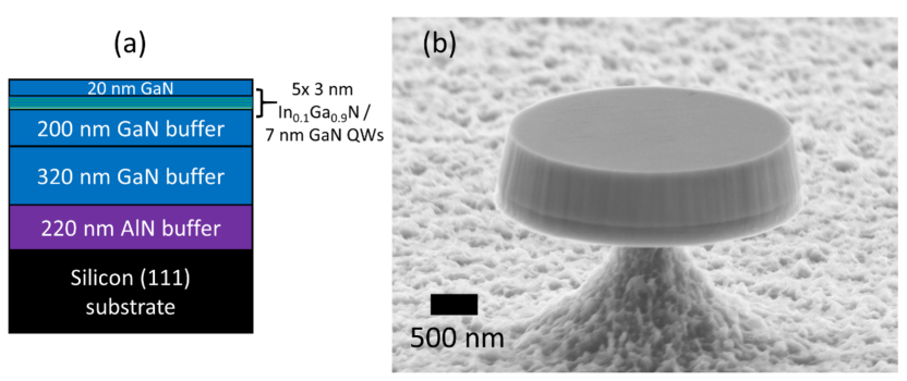
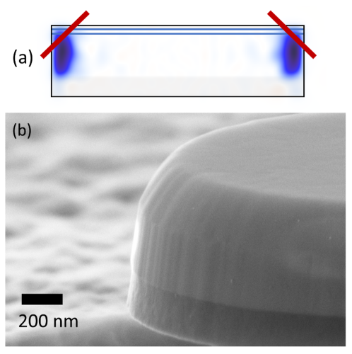
The investigated sample was grown by metal organic chemical vapor deposition (MOCVD) on Si (111). In a first growth run, a template was grown consisting of 220 nm AlN and 320 nm GaN. Then in a second growth run another 200 nm of GaN were grown, followed by the active region consisting of 3 nm In0.1Ga0.9N / 7 nm GaN QWs, and a 20 nm GaN cap layer. The total thickness is 810 nm. A schematic of the heterostructure is depicted in Fig. 1 (a). The threading dislocation density is estimated to be from a atomic force microscopy image (see Fig. S1 in the supplementary material), a standard value for thin III-nitride layers grown on Si. A photoluminescence (PL) measurement of the as-grown sample is shown in Fig. S2 of the supplementary material, showing QW emission centered around 428 nm. We fabricated microdisks using standard cleanroom processing. We used a plasma enhanced chemical vapor deposition (PECVD) SiO2 hard mask, e-beam lithography using UV5 positive resist, and inductively coupled plasma (ICP) etching using CH2F2 and CF4 gases for the SiO2 and Cl2 and BCl3 gases for the III-nitride. The Si was underetched using XeF2 gas. A scanning electron microscope (SEM) image of a diameter disk is depicted in Fig. 1 (b), showing smooth slightly-inclined side-walls.
We use a standard -PL setup with a 355 nm pulsed laser (4 ns pulse width, 7 kHz repetition rate) and a microscope objective to both pump the microdisk and collect its emission from the top. A spectrometer and a Peltier-cooled charge coupled device (CCD) are used as the detector.
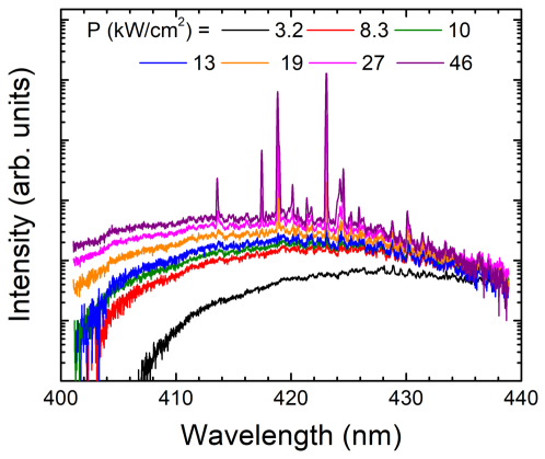
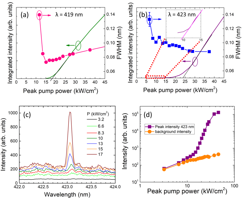
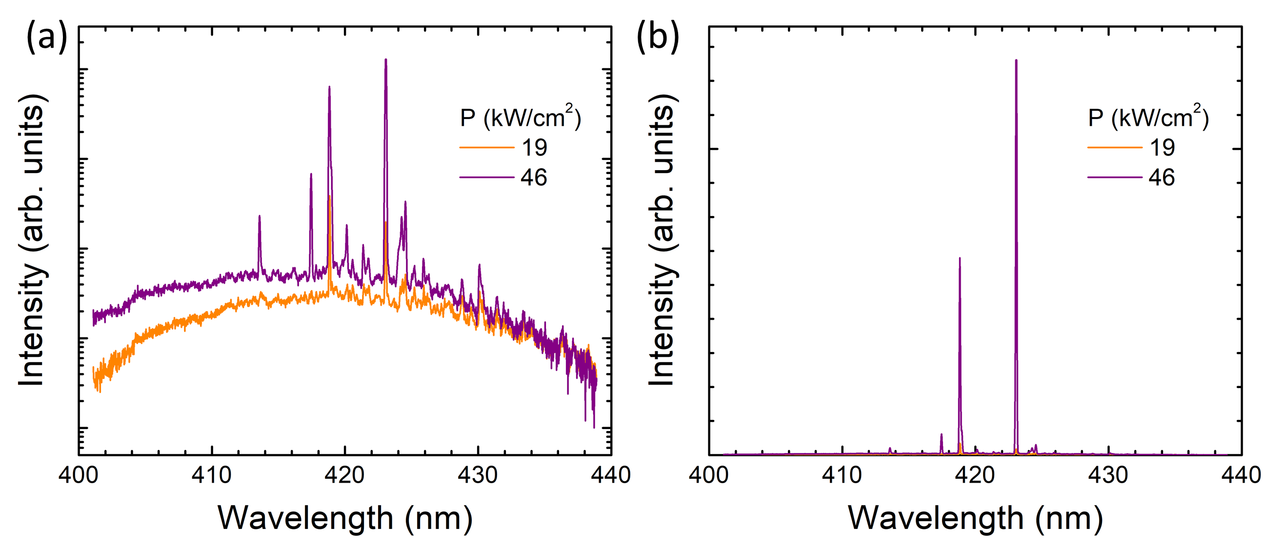
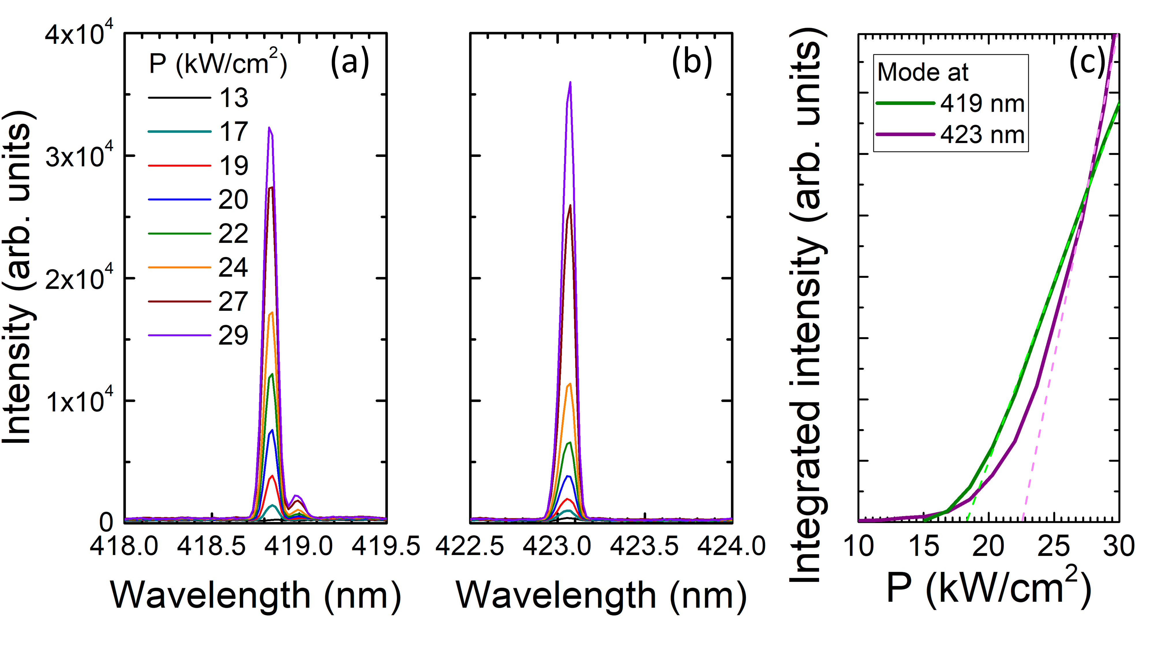
Fig. 2 shows pump power dependent spectra of a diameter disk. Several modes are lasing and we can see clamping of the spontaneous emission at low energy (see Fig. S3 in the supplementary material). The two strongest modes at 419 and 423 nm have very similar thresholds and are in strong competition. Figs. 3 (a) and (b) show the integrated intensity and linewidth over peak pump power for the modes at 419 and 423 nm, respectively. We point out the limited visibility of whispering-gallery modes (WGMs) below threshold in a top-collection setup, as WGMs radiate preferentially in-plane. For the mode at 419 nm (Fig. 3 (a)), the narrowest linewidth of 0.07 nm is observed at peak power and the threshold is around (or threshold energy per pulse of ). At higher power densities, a second mode appears at nearly the same wavelength (see Fig. S4 in the supplementary material), thus making the linewidth analysis complex. For the mode at 423 nm (Fig. 3 (b)), the linewidth starts narrowing at . A zoom of the low power range of -, given in Fig. 3 (c), shows the onset of the mode dynamics and indicates a threshold at consistent with the linewidth narrowing. There is nonetheless mode competition with the 419 nm mode, which is discussed in more detail in the supplementary material (Fig. S5). Consequently, Fig. 3 (b)) indicates an overall threshold to be around . A close-up of the mode at 423 nm at low pump powers below threshold is shown in Fig. 3 (c). A large dynamic between the peak intensity and the background spontaneous emission of can be discerned for the 423 nm mode in Fig. 3 (d), where we plot the peak and background intensities over pump power in a double logarithmic plot. At the last point of the CCD is saturated.
Using the rate equation model introduced by Baba and Sano, we get the following formula for the threshold power Baba and Sano (2003):
| (1) |
with the photon energy of the pump laser, the total thickness of the active medium, the ratio between the homogeneous broadening of the laser mode and the spectral broadening of the spontaneous emission Baba and Sano (2003), the injection efficiency of the carriers into the QWs, the surface reflectivity, the spontaneous emission factor, the spontaneous emission lifetime, the non-radiative lifetime, and the threshold carrier density, which is given by
| (2) |
where is the transparency carrier density, the group index, the speed of light, the overlap of the optical mode with the QWs, the dynamic gain, and the photon lifetime. Equation 2 indicates that the first requirement to obtain a net positive gain is to reach transparency. Once transparency is attained, another important factor to reach threshold is . For the TE0 mode, we calculate for our 5 QWs (see Fig. S6 in the supplementary material), which is very small and could be improved in future work. We calculate and is given by , where is an empirical gain coefficient, which we estimate to be , based on Ref. Vico Triviño et al. (2015), where they study a fairly similar QW (3 nm, 15% In) and which constitutes a typical value. For more information on the threshold gain, refer to the supplementary material.
The photon lifetime is given by
| (3) |
with the quality factor and the peak wavelength. We calculate using the below threshold linewidth, which is in good agreement with our previous samples Sellés et al. (2016b); Tabataba-Vakili et al. (2019a), and . We get .
The sheet transparency carrier density is around for InGaN QWs, which gives us for our 3 nm QWs Chow, Wright, and Nelson (1996); Hangleiter et al. (1997); Vico Triviño et al. (2015). Using Eq. 2, we thus get .
We can calculate using Baba and Sano (2003)
| (4) |
where is the polarization anisotropy of the spontaneous emission, is the relative confinement factor, is the effective refractive index, is the mode volume, and is the homogeneous broadening of the QW emission. We calculate the mode volume using the finite-difference time-domain (FDTD) method with and obtain for a first order radial TE0 mode. Note that this weak mode volume is linked to the short wavelength investigated. Using (consistent with the formula for , the spontaneous emission factor, in Ref. Coldren, Corzine, and Masanovic (2012), p. 562), (for a cavity with many modes Baba (1997)), , and , we get . This value is still fairly small and can thus be neglected in Eq. 1.
Note that , the spontaneous emission factor, is in first approximation inversely proportional to the number of allowed cavity modes in the spectral broadening. This spontaneous emission factor is in the literature often presented as Vico Triviño et al. (2015); Sellés et al. (2016b); Athanasiou et al. (2014). By accounting for the homogeneous broadening in the calculation of , we assume to be in the so-called bad emitter regime, i.e. emitter linewidth larger than the cavity linewidth Van Exter, Nienhuis, and Woerdman (1996); Coldren, Corzine, and Masanovic (2012). Note that Eq. 1 is the same as in Ref. Coldren, Corzine, and Masanovic (2012) (p. 252) except for the pre-factor that accounts for homogeneous broadening.
Using the standard rate equations given in Ref. Coldren, Corzine, and Masanovic (2012) (p. 249), we can fit the L-L curve of Fig. 3 (b) in the range up to . We obtain a value of for the spontaneous emission factor, which is within a factor of 3 of the calculated value of . For the here presented range of microdisk parameters the equations for the laser threshold are equivalent to those for ridge waveguide lasers Morkoç (2009); Coldren, Corzine, and Masanovic (2012) where the spontaneous emission factor is weak.
for our pump laser and for our 5 QWs. The reflectivity of GaN at 355 nm is 19% Kawashima et al. (1997). We can estimate and using the ABC model Scheibenzuber et al. (2011) with
| (5) |
where the first term describes Shockley-Read-Hall recombination, the second term describes radiative recombination, and the third term describes Auger-type recombination. We use , , and (see Refs. Scheibenzuber et al. (2011); Vico Triviño et al. (2015)). As discussed below, there is a large spread on these values in the literature. We use the aforementioned values because they have been measured for InGaN laser diodes emitting in the same spectral range as our sample and at high carrier densities. However, the laser diodes studied by Scheibenzuber et al. Scheibenzuber et al. (2011) were grown on bulk GaN, thus having a much smaller dislocation density than our material, which has an influence on the non-radiative lifetime. Assuming a 5 times larger would increase by a factor of 2, a 10 times larger would result in a factor 3 increase in . Given that our measured thresholds are quite low, the non-radiative lifetime cannot be extremely short. At threshold, we calculate , , and using the ABC values of Scheibenzuber et al. Scheibenzuber et al. (2011). It corresponds to an internal quantum efficiency of 24% at threshold. This is very close to and a bit larger than the pulse width of 4 ns, which can influence the carrier dynamics and increase the threshold. Meanwhile, a 5 times larger would result in a of , which is significantly shorter than the pulse width, and a factor 2 larger , which would still fit well with our experimental values. Our threshold calculation assumes a pseudo-continuous modeling. In the supplementary material, we compare the carrier lifetimes and thresholds obtained for the ABC values of Scheibenzuber et al. Scheibenzuber et al. (2011) and Espenlaub et al. Espenlaub et al. (2019) for our sample as well as the samples of Refs. Tamboli et al. (2007) and Vico Triviño et al. (2015).
The parameters and in Eq. 1 are not well-known. is the ratio between the homogeneous broadening and the spectral broadening. It is unlikely that all the spontaneous emission participates homogeneously to the laser mode, and is certainly less than one. Under non-resonant optical pumping, the carriers are photo-induced in the barriers and subsequently captured in the QWs. Moreover, at room temperature, a fraction of the carriers can thermally escape from the QWs. There are 5 QWs in our active structure. Considering a value of 0.4 (for a spectral broadening of 35 nm and a homogeneous broadening of 15 nm) and a large range of between 0.3 and 0.7, their product is likely in the 0.1-0.3 range.
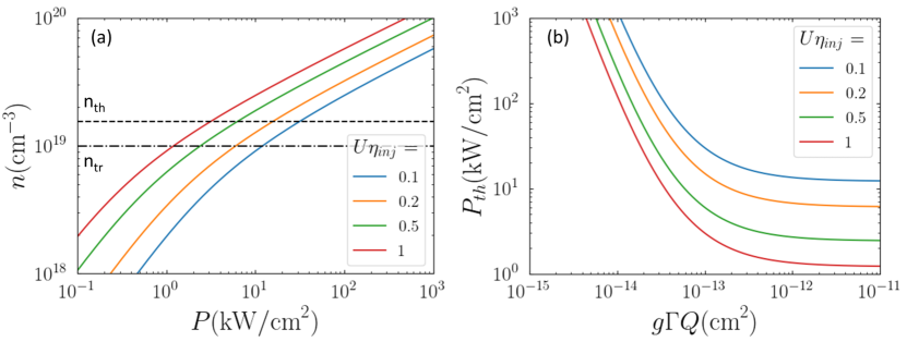
In Fig. 4 (a), we plot over below threshold for different values of between 0.1 and 1 using Eqs. 1 (which is valid below and at threshold) and 5. The values of and of our sample are indicated. For , we get , which is the value we observed experimentally, indicating that the parameters considered for the III-nitride microresonators on silicon are relevant. We cannot be sure which vertical mode order is lasing. For the TE1 mode, we would have a larger value of , , and the same value would be attained for a smaller value of of 0.1. A different vertical order would also imply a different mode volume. A would correspond to a .
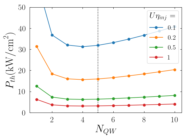
In Fig. 4 (b), we plot as a function of using Eqs. 1, 2, 3, and 5. High gain, high Q and strong overlap are parameters governing the threshold. For large values of (i.e. for a very high-Q cavity), goes towards , the power needed to reach transparency. We can see that even for an unrealistic at room temperature, is still . Using a single QW, as opposed to 5, can reduce the minimum power needed to reach transparency to . We recall that for III-nitrides the relatively large threshold values as compared to other compound semiconductors are directly associated to the large density of states due to the heavy electron and holes effective masses characteristic of III-nitrides.
In Fig. S7 in the supplementary information, we show as a function of the number of QWs.
While low-threshold lasing has been demonstrated under electrical injection Kozaki et al. (2006), we note that care needs to be taken when comparing such lasing thresholds with those measured under optical pumping. M. Martens Martens (2018) (p. 32-33) reported for virtually identical structures a threshold of under optical pumping at 266 nm and under electrical injection. We can estimate the expected threshold current density of an equivalent structure to ours using Rosencher and Vinter (2004) (p. 635)
| (6) |
where is the elementary charge, and using , , and and obtain for an ideal electrical injection, whereas we have measured under optical pumping.
Achieving a threshold below for a multi-QW (MQW) at room temperature is thus highly challenging. In the literature, a claim of lasing at threshold powers as low as at a similar wavelength and for a comparable active region (also 5 QWs) was reported in Ref. Tamboli et al. (2007). They demonstrate a dynamic between peak and background of only a factor of around 8 at , which is 40 times smaller than in our case. We need to consider the large variability of ABC parameters in literature Piprek (2010); Karpov (2015); Espenlaub et al. (2019); David et al. (2019). In order to achieve with the parameters of the sample reported by Tamboli et al. Tamboli et al. (2007), a of 110 ns would be required at , which would require to be around one order of magnitude smaller as compared to the values of Scheibenzuber et al. Scheibenzuber et al. (2011), along with a smaller value and a much smaller value, i.e. very long radiative lifetimes and high material quality leading to very long non-radiative lifetimes. We discuss different ABC parameters and resulting calculated thresholds in the supplementary material. This radiative lifetime improvement could be combined with an increase of the factor by decreasing the cavity size. If a different gain medium was studied, i.e. quantum dots instead of QWs, or generally more localized emitters, the density of states would be different Arakawa and Sakaki (1982), and the threshold could possibly be reduced since would be lower. Localized states are expected in InGaN QWs, but for the pump powers reported by Tamboli et al. Tamboli et al. (2007) or in this work, it is expected that they are saturated and that a 2D density of states is recovered, thus justifying the QW rate equation analysis.
The here discussed linewidth of 0.07 nm at threshold is one of the narrowest values reported for III-nitride microdisks. The only smaller value we found, 0.033 nm, was reported by Simeonov et al. Simeonov et al. (2007, 2008) for III-nitride microdisks on sapphire with a higher threshold of . As for III-nitride microdisk lasers on silicon, we have not found any narrower values.
While even a perfect resonator cannot infinitely reduce the threshold, a badly processed microdisk can easily result in no lasing being observed at all. Fig. 5 (a) shows a schematic of the cross-section of a diameter disk depicting the field of a first order radial mode (for a perfect microdisk) and indicating truncated edges that strongly reduce the overlap of the mode with the QWs, which are at the top of the structure, not taking into account that the truncated edges would also change the mode profile a bit. In Fig. 5 (b) we show an SEM image of such a disk, which does not lase under pulsed optical pumping. We have also observed an order of magnitude difference in threshold for microdisks on two samples separately processed from the same wafer, highlighting the need for a high quality cavity.
We did not observe CW lasing for our sample, which is likely due to the fact that our microdisks are fairly large ( diameter) and our CW laser is not sufficiently powerful. Meanwhile, CW lasing is always challenging for microdisk structures due to thermal management and pedestal size. A weak dependence of threshold vs. temperature is also mandatory and will be the subject of future work.
In conclusion, we have demonstrated low threshold ( peak power) pulsed optically pumped lasing in III-nitride microdisks grown by MOCVD on Si with a narrow linewidth and a large peak to background dynamic of 300. We calculated the threshold power using a rate equation model and obtained values that are in good agreement with our measurements, which highlights the fact that InGaN MQWs require a minimum power in the order of kW/cm2 to reach the transparency carrier density. The presented microresonators fabricated on Si are thus close to the best that can be achieved with III-nitride QWs.
Supplementary material
See the supplementary material for material characterization, additional lasing spectra, a 1D simulation of the mode overlap, a discussion of the threshold gain, a discussion of the dependence of the threshold on the number of QWs, as well as a discussion of the calculated lasing thresholds using different ABC values.
Acknowledgements.
We thank Damir Vodenicarevic for his help with python scripts for data analysis. This work was supported by the French Agence Nationale de la Recherche (ANR) under MILAGAN convention (ANR-17-CE08-0043-02). We acknowledge support by a public grant overseen by the ANR as part of the “Investissements d’Avenir” program: Labex GANEX (Grant No. ANR-11-LABX-0014). This work was also partly supported by the RENATECH network. We acknowledge the support from the technical teams at PTA-Grenoble and Nanofab (Institut Néel).Data availability
The data that supports the findings of this study are available within the article [and its supplementary material].
References
- McCall et al. (1992) S. L. McCall, A. F. J. Levi, R. E. Slusher, S. J. Pearton, and R. A. Logan, “Whispering-gallery mode microdisk lasers,” Appl. Phys. Lett. 60, 289–291 (1992).
- Islim et al. (2017) M. S. Islim, R. X. Ferreira, X. He, E. Xie, S. Videv, S. Viola, S. Watson, N. Bamiedakis, R. V. Penty, I. H. White, A. E. Kelly, E. Gu, H. Haas, and M. D. Dawson, “Towards 10 Gb/s orthogonal frequency division multiplexing-based visible light communication using a GaN violet micro-LED,” Photonics Res. 5, A35–A43 (2017).
- Estevez, Alvarez, and Lechuga (2012) M. C. Estevez, M. Alvarez, and L. M. Lechuga, “Integrated optical devices for lab-on-a-chip biosensing applications,” Laser & Photonics Reviews 6, 463–487 (2012).
- Butté and Grandjean (2020) R. Butté and N. Grandjean, “III-nitride photonic cavities,” Nanophotonics 9, 569–598 (2020).
- Haberer et al. (2004) E. D. Haberer, R. Sharma, C. Meier, A. R. Stonas, S. Nakamura, S. P. DenBaars, and E. L. Hu, “Free-standing, optically pumped, GaN/InGaN microdisk lasers fabricated by photoelectrochemical etching,” Appl. Phys. Lett. 84, 5179–5181 (2004).
- Simeonov et al. (2007) D. Simeonov, E. Feltin, H.-J. Bühlmann, T. Zhu, A. Castiglia, M. Mosca, J.-F. Carlin, R. Butté, and N. Grandjean, “Blue lasing at room temperature in high quality factor GaN/AlInN microdisks with InGaN quantum wells,” Appl. Phys. Lett. 90, 061106 (2007).
- Simeonov et al. (2008) D. Simeonov, E. Feltin, A. Altoukhov, A. Castiglia, J.-F. Carlin, R. Butté, and N. Grandjean, “High quality nitride based microdisks obtained via selective wet etching of AlInN sacrificial layers,” Appl. Phys. Lett. 92, 171102 (2008).
- Aharonovich et al. (2013) I. Aharonovich, A. Woolf, K. J. Russell, T. Zhu, N. Niu, M. J. Kappers, R. A. Oliver, and E. L. Hu, “Low threshold, room-temperature microdisk lasers in the blue spectral range,” Appl. Phys. Lett. 103, 021112 (2013).
- Sellés et al. (2016a) J. Sellés, C. Brimont, G. Cassabois, P. Valvin, T. Guillet, I. Roland, Y. Zeng, X. Checoury, P. Boucaud, M. Mexis, F. Semond, and B. Gayral, “Deep-UV nitride-on-silicon microdisk lasers,” Sci. Rep. 6, 21650 (2016a).
- Sellés et al. (2016b) J. Sellés, V. Crepel, I. Roland, M. El Kurdi, X. Checoury, P. Boucaud, M. Mexis, M. Leroux, B. Damilano, S. Rennesson, F. Semond, B. Gayral, C. Brimont, and T. Guillet, “III-nitride-on-silicon microdisk lasers from the blue to the deep ultra-violet,” Appl. Phys. Lett. 109, 231101 (2016b).
- Zhu et al. (2020) G. Zhu, J. Li, N. Zhang, X. Li, J. Dai, Q. Cui, Q. Song, C. Xu, and Y. Wang, “Whispering-gallery mode lasing in a floating GaN microdisk with a vertical slit,” Sci. Rep. 10, 253 (2020).
- Tamboli et al. (2007) A. C. Tamboli, E. D. Haberer, R. Sharma, K. H. Lee, S. Nakamura, and E. L. Hu, “Room-temperature continuous-wave lasing in GaN/InGaN microdisks,” Nature Photonics 1, 61–64 (2007).
- Athanasiou et al. (2014) M. Athanasiou, R. Smith, B. Liu, and T. Wang, “Room temperature continuous-wave green lasing from an InGaN microdisk on silicon,” Sci. Rep. 4, 7250 (2014).
- Athanasiou et al. (2017) M. Athanasiou, R. M. Smith, J. Pugh, Y. Gong, M. J. Cryan, and T. Wang, “Monolithically multi-color lasing from an InGaN microdisk on a Si substrate,” Sci. Rep. 7, 10086 (2017).
- Mexis et al. (2011) M. Mexis, S. Sergent, T. Guillet, C. Brimont, T. Bretagnon, B. Gil, F. Semond, M. Leroux, D. Néel, S. David, X. Checoury, and P. Boucaud, “High quality factor nitride-based optical cavities: microdisks with embedded GaN/Al(Ga)N quantum dots,” Optics Letters 36, 2203–2205 (2011).
- Rousseau et al. (2018) I. Rousseau, G. Callsen, G. Jacopin, J.-F. Carlin, R. Butté, and N. Grandjean, “Optical absorption and oxygen passivation of surface states in III-nitride photonic devices,” J. Appl. Phys. 123, 113103 (2018).
- Kneissl et al. (2004) M. Kneissl, M. Teepe, N. Miyashita, N. M. Johnson, G. D. Chern, and R. K. Chang, “Current-injection spiral-shaped microcavity disk laser diodes with unidirectional emission,” Appl. Phys. Lett. 84, 2485–2487 (2004).
- Feng et al. (2018) M. Feng, J. He, Q. Sun, H. Gao, Z. Li, Y. Zhou, J. Liu, S. Zhang, D. Li, L. Zhang, X. Sun, D. Li, H. Wang, M. Ikeda, R. Wang, and H. Yang, “Room-temperature electrically pumped InGaN based microdisk laser grown on Si,” Opt. Express 26, 5043–5051 (2018).
- Wang et al. (2019) J. Wang, M. Feng, R. Zhou, Q. Sun, J. Liu, Y. Huang, Y. Zhou, H. Gao, X. Zheng, M. Ikeda, and H. Yang, “GaN-based ultraviolet microdisk laser diode grown on Si,” Photonics Research 7, B32–B35 (2019).
- Wang et al. (2020) J. Wang, M. Feng, R. Zhou, Q. Sun, J. Liu, X. Sun, X. Zheng, M. Ikeda, X. Sheng, and H. Yang, “Continuous-wave electrically injected GaN-on-Si microdisk laser diodes,” Optics Express 28, 12201–12208 (2020).
- Tabataba-Vakili et al. (2018) F. Tabataba-Vakili, L. Doyennette, C. Brimont, T. Guillet, S. Rennesson, E. Frayssinet, B. Damilano, J.-Y. Duboz, F. Semond, I. Roland, M. El Kurdi, X. Checoury, S. Sauvage, B. Gayral, and P. Boucaud, “Blue microlasers integrated on a photonic platform on silicon,” ACS Photonics 5, 3643–3648 (2018).
- Tabataba-Vakili et al. (2019a) F. Tabataba-Vakili, L. Doyennette, C. Brimont, T. Guillet, S. Rennesson, B. Damilano, E. Frayssinet, J.-Y. Duboz, X. Checoury, S. Sauvage, M. El Kurdi, F. Semond, B. Gayral, and P. Boucaud, “Demonstration of critical coupling in an active III-nitride microdisk photonic circuit on silicon,” Sci. Rep. 9, 18095 (2019a).
- Tabataba-Vakili et al. (2020) F. Tabataba-Vakili, B. Alloing, B. Damilano, H. Souissi, C. Brimont, L. Doyennette, T. Guillet, X. Checoury, M. E. Kurdi, S. Chenot, E. Frayssinet, J.-Y. Duboz, F. Semond, B. Gayral, and P. Boucaud, “Monolithic integration of ultraviolet microdisk lasers into photonic circuits in a III-nitride-on-silicon platform,” Opt. Lett. 45, 4276–4279 (2020).
- Tabataba-Vakili et al. (2019b) F. Tabataba-Vakili, S. Rennesson, B. Damilano, E. Frayssinet, J.-Y. Duboz, F. Semond, I. Roland, B. Paulillo, R. Colombelli, M. El Kurdi, X. Checoury, S. Sauvage, L. Doyennette, C. Brimont, T. Guillet, B. Gayral, and P. Boucaud, “III-nitride on silicon electrically injected microrings for nanophotonic circuits,” Opt. Express 27, 11800–11808 (2019b).
- Baba and Sano (2003) T. Baba and D. Sano, “Low-threshold lasing and Purcell effect in microdisk lasers at room temperature,” IEEE J. Sel. Top. Quantum Electronics 9, 1340–1346 (2003).
- Vico Triviño et al. (2015) N. Vico Triviño, R. Butté, J.-F. Carlin, and N. Grandjean, “Continuous wave blue lasing in III-nitride nanobeam cavity on silicon,” Nano Lett. 15, 1259–1263 (2015).
- Chow, Wright, and Nelson (1996) W. Chow, A. Wright, and J. Nelson, “Theoretical study of room temperature optical gain in GaN strained quantum wells,” Applied physics letters 68, 296–298 (1996).
- Hangleiter et al. (1997) A. Hangleiter, G. Frankowsky, V. Härle, and F. Scholz, “Optical gain in the nitrides: are there differences to other III–V semiconductors?” Materials Science and Engineering: B 43, 201–206 (1997).
- Coldren, Corzine, and Masanovic (2012) L. A. Coldren, S. W. Corzine, and M. L. Masanovic, Diode lasers and photonic integrated circuits, Vol. 218 (John Wiley & Sons, Hoboken, New Jersey, 2012).
- Baba (1997) T. Baba, “Photonic crystals and microdisk cavities based on GaInAsP-InP system,” IEEE journal of selected topics in quantum electronics 3, 808–830 (1997).
- Van Exter, Nienhuis, and Woerdman (1996) M. Van Exter, G. Nienhuis, and J. Woerdman, “Two simple expressions for the spontaneous emission factor ,” Physical Review A 54, 3553–3558 (1996).
- Morkoç (2009) H. Morkoç, Handbook of Nitride Semiconductors and Devices: GaN-based optical and electronic devices (Wiley-VCH, Weinheim, 2009).
- Kawashima et al. (1997) T. Kawashima, H. Yoshikawa, S. Adachi, S. Fuke, and K. Ohtsuka, “Optical properties of hexagonal GaN,” Journal of Applied Physics 82, 3528–3535 (1997).
- Scheibenzuber et al. (2011) W. Scheibenzuber, U. Schwarz, L. Sulmoni, J. Dorsaz, J.-F. Carlin, and N. Grandjean, “Recombination coefficients of GaN-based laser diodes,” Journal of Applied Physics 109, 093106 (2011).
- Espenlaub et al. (2019) A. C. Espenlaub, D. J. Myers, E. C. Young, S. Marcinkevičius, C. Weisbuch, and J. S. Speck, “Evidence of trap-assisted Auger recombination in low radiative efficiency MBE-grown III-nitride LEDs,” Journal of Applied Physics 126, 184502 (2019).
- Kozaki et al. (2006) T. Kozaki, H. Matsumura, Y. Sugimoto, S.-i. Nagahama, and T. Mukai, “High-power and wide wavelength range GaN-based laser diodes,” in Novel In-Plane Semiconductor Lasers V, Vol. 6133 (International Society for Optics and Photonics, 2006) p. 613306.
- Martens (2018) M. Martens, Optical gain and modal loss in AlGaN based deep UV lasers, Ph.D. thesis, Technische Universität Berlin (2018).
- Rosencher and Vinter (2004) E. Rosencher and B. Vinter, Optoelectronics (Cambridge University Press, Cambridge, 2004).
- Piprek (2010) J. Piprek, “Efficiency droop in nitride-based light-emitting diodes,” physica status solidi (a) 207, 2217–2225 (2010).
- Karpov (2015) S. Karpov, “ABC-model for interpretation of internal quantum efficiency and its droop in III-nitride LEDs: a review,” Optical and Quantum Electronics 47, 1293–1303 (2015).
- David et al. (2019) A. David, N. G. Young, C. Lund, and M. D. Craven, “The physics of recombinations in III-nitride emitters,” ECS Journal of Solid State Science and Technology 9, 016021 (2019).
- Arakawa and Sakaki (1982) Y. Arakawa and H. Sakaki, “Multidimensional quantum well laser and temperature dependence of its threshold current,” Applied Physics Letters 40, 939–941 (1982).
- (43) “OMS: 1-D mode solver for dielectric multilayer slab waveguides,” https://www.computational-photonics.eu/oms.html, accessed: 2020-02-28.
Supplementary information for
Analysis of low-threshold optically pumped III-nitride microdisk lasers
Farsane Tabataba-Vakili,1,2 Christelle Brimont,3 Blandine Alloing,4 Benjamin Damilano,4 Laetitia Doyennette,3 Thierry Guillet,3 Moustafa El Kurdi,1 Sébastien Chenot,4 Virginie Brändli,4 Eric Frayssinet,4 Jean-Yves Duboz,4 Fabrice Semond,4 Bruno Gayral2 and Philippe Boucaud4,∗
1Université Paris-Saclay, CNRS, C2N, 91120, Palaiseau, France.
2Univ. Grenoble Alpes, CEA, IRIG-Pheliqs, 38000 Grenoble, France.
3L2C, Université de Montpellier, CNRS, 34095 Montpellier, France.
4Université Côte d’Azur, CNRS, CRHEA, 06560 Valbonne, France.
∗Electronic address: philippe.boucaud@crhea.cnrs.fr
Material characterization
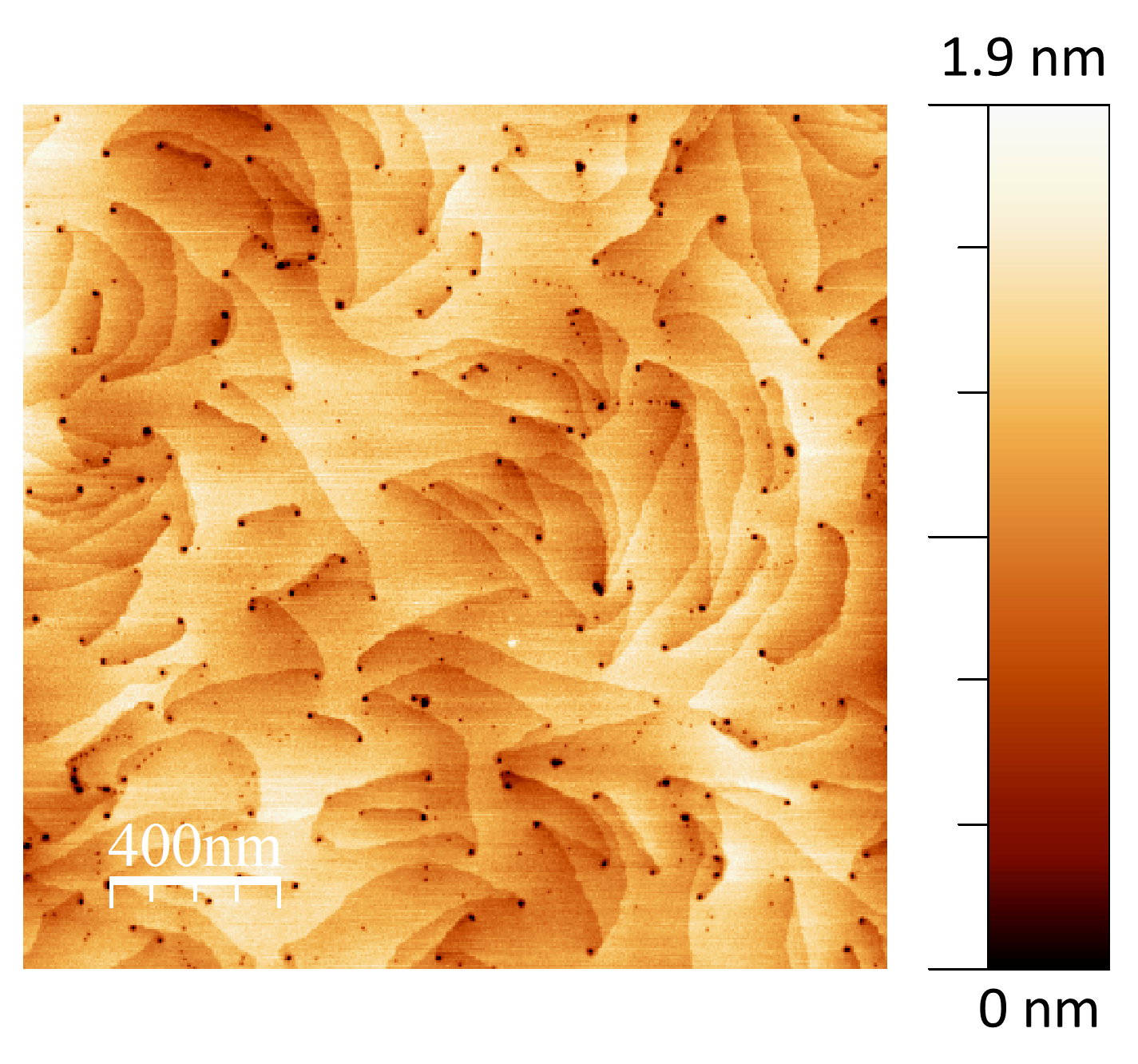
Fig. S1 shows a atomic force microscopy (AFM) image of the sample discussed in the main text with a threading dislocation density (TDD) of . This is a typical value for thin III-nitride layers on silicon substrate.
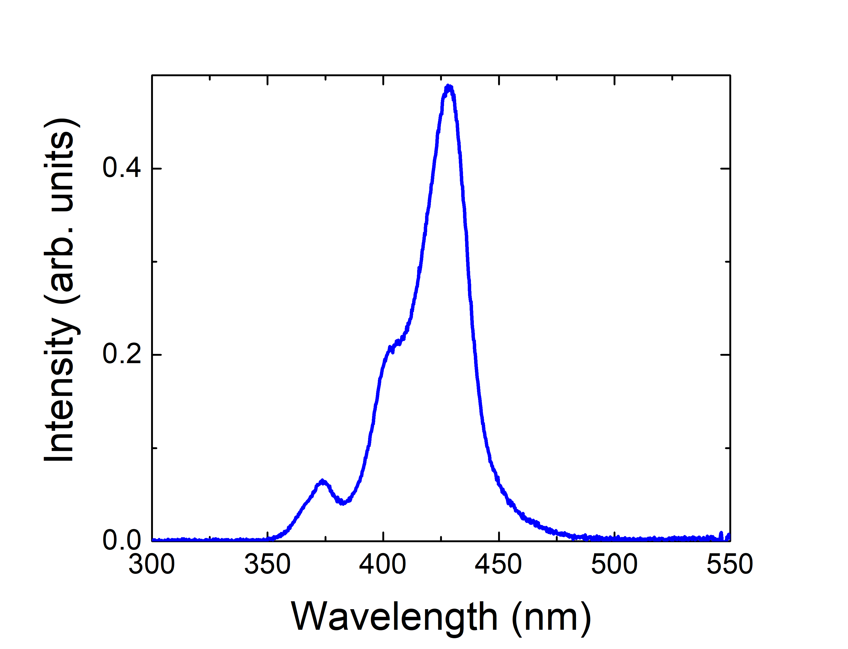
Fig. S2 shows a room temperature high excitation power density -photoluminescence (-PL) spectrum of the as-grown sample using a 266 nm pump laser with 400 ps pulse width and 7 kHz repetition rate, measured at . The QW emission is centered around 428 nm with a shoulder at 400 nm that is likely related to the emission of excited states. We further observe emission from the tensile strained GaN buffer layer around 373 nm. The full width at half maximum (FWHM) of the main resonance is 22 nm. The main lasing peaks are observed around 423 nm, i.e. on the high-energy side of the -PL spectra.
Lasing spectra
The lasing experiments were performed using a 55 cm focal length spectrometer, with a grating with 1200 lines/mm. The spectral resolution is 0.3 meV, 0.04 nm. The laser spot size was 6 m.
Fig. S3 shows two lasing spectra of Fig. 2 in the main text at pump powers of 19 and with (a) a logarithmic and (b) a linear intensity axis to more clearly show the clamping of the background emission in the low energy range (long wavelength). At shorter wavelength the background emission is not fully clamped due to inhomogeneous spectral broadening. The peak to background dynamic is in the range of 300 at , that is . In Ref. Tamboli et al. (2007), they only demonstrate a factor of around 8 at .
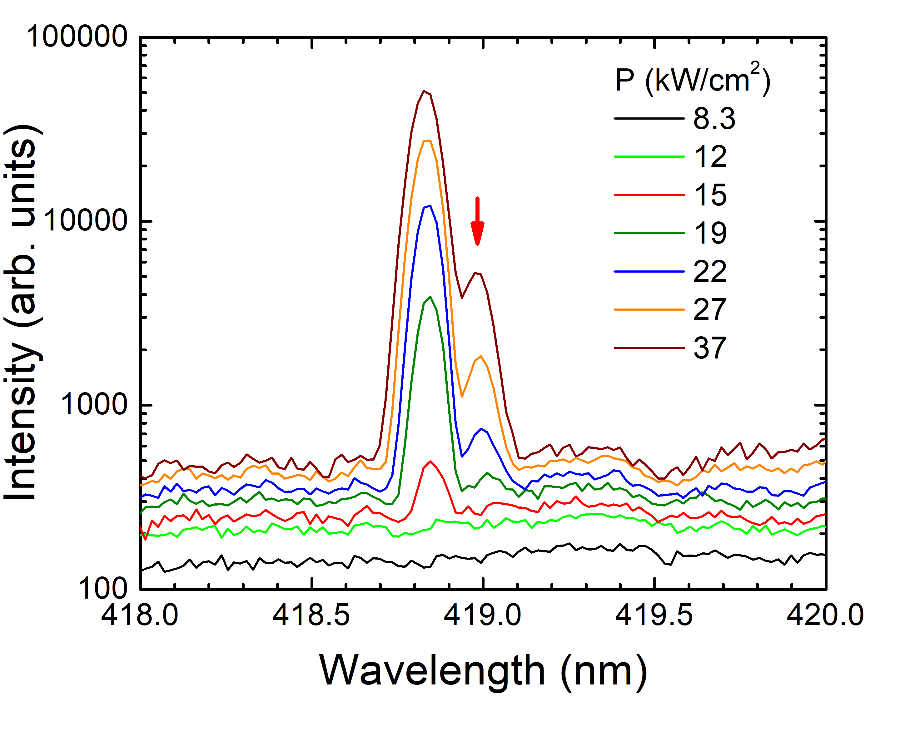
Fig. S4 shows a close-up of the spectra in Fig. 2 around 419 nm. As described in the main text, a second lasing mode appears at higher excitation power at nearly the same wavelength, making the linewidth analysis more complex.
Figs. S5 (a) and (b) show the modes at 419 nm and 423 nm, respectively. While initially the mode at 423 nm is more intense, the mode at 419 nm becomes stronger at around 17 kW/cm2. Then at around 29 kW/cm2, the mode at 423 nm takes over again. This mode competiton can also clearly be seen in Fig. S5 (c), which shows the integrated intensity over pump power for both modes.
Mode overlap
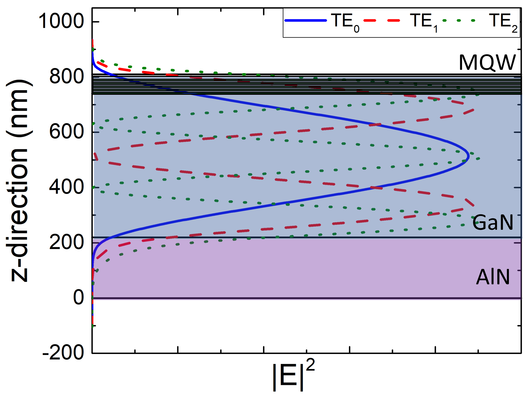
Figure S6 shows the overlap of the TE0, TE1, and TE2 modes with the 5 QWs in a 1D slab waveguide determined using a 1D mode solver OMS . The overlap of the 5 QWs with the modes is 0.44%, 1.6%, 2.8% for the TE0, TE1, and TE2 modes, respectively. Using the same approach, we have calculated an overlap factor of for the structure investigated in Ref. Tamboli et al. (2007), assuming a quantum well width of 4 nm, which was not indicated in their article and is based on information in a previous publication Haberer et al. (2004).
Discussion of the threshold gain
The carrier density at threshold can be described by a different equivalent set of equations. Eq. 2 in the main text can be rewritten as
| (S1) |
where is the threshold gain that is given by
| (S2) |
We assume a constant 2D transparency carrier density of and an empirical gain coefficient (Ref. Vico Triviño et al. (2015)) for our sample and the results of Refs. Tamboli et al. (2007); Vico Triviño et al. (2015). The 3D transparency carrier density is given by , where is the thickness of 1 QW.
Using the values , , that we give in the main text for our sample, we obtain . This gives us a factor of between and .
Meanwhile, for Ref. Vico Triviño et al. (2015), using , , and that they indicate, we obtain using Eq. 3 in the main text, and and using Eqs. S1 and S2, which matches well with the values reported in their article.
For Ref. Tamboli et al. (2007), we obtain and using , calculated from the structure given in Ref. Haberer et al. (2004), and and , i.e. , as indicated in Ref. 12. A much stronger overlap factor of the quantum wells leads to a much smaller difference between and . Note that there is only a factor 2 for the threshold carrier density between our work and Ref. Tamboli et al. (2007). This is based on the assumption that the QWs in Tamboli et al. are 4 nm thick, which is not explicitly stated. If they are thinner, is larger and is smaller.
Furthermore, in a less approximated form, Eq. S1 can also be written as
| (S3) |
Dependence of the lasing threshold on QW number
The lasing threshold has a double dependence on the number of QWs, . There is a linear dependence that can be seen in Eq. 1 in the main text, as the total thickness of the active region is given by . The second non-linear dependence is given in Eq. 2 in the main text, as also depends on the QW number and is in first approximation given as where is the overlap for one single quantum well.
The lasing threshold is thus given by
| (S4) |
Fig. S7 shows as a function of . A minimum can be observed for around 3-4 QWs. However, our 5 QWs are not far from this optimal value for the here considered heterostructure.
Lasing thresholds for different ABC values
As discussed in the main text, there is a large variation in the ABC parameters in literature. This variation is obviously a signature of the heterostructure quality and design, including the In content of the layers. We compare the carrier lifetimes and lasing thresholds obtained with the ABC values taken from two articles Scheibenzuber et al. (2011); Espenlaub et al. (2019) for our sample as well as the results reported in literature Tamboli et al. (2007); Vico Triviño et al. (2015). Then we further discuss the results of Tamboli et al. Tamboli et al. (2007) using the ABC model discussed by David et al. David et al. (2019).
| This work | Vico Triviño et al. Vico Triviño et al. (2015) | Tamboli et al. Tamboli et al. (2007) | ||
|---|---|---|---|---|
| (ns) | 5.1 | 6.7 | 11 | |
| (kW/cm 2) | 0.2 | 16 | 2.6 | 5.3 |
| (kW/cm 2) | 0.5 | 6.4 | 1.0 | 2.1 |
| (kW/cm 2) (experimental) | 18 | 0.74 | 0.3 |
Table S1 shows and calculated using the ABC values of Scheibenzuber et al. Scheibenzuber et al. (2011) for our samples as well as for Refs. Vico Triviño et al. (2015); Tamboli et al. (2007) for two different values of . The ABC values of Scheibenzuber et al. were obtained around threshold from laser diodes emitting around 415 nm.
Next, we consider the ABC values of Espenlaub et al. (Ref. 35) (, , and ), which were obtained for MBE-grown LEDs on sapphire with low efficiency quantum wells. Table S2 shows and calculated using these ABC values for our samples as well as for Refs. Vico Triviño et al. (2015); Tamboli et al. (2007) for two different values of .
| This work | Vico Triviño et al. Vico Triviño et al. (2015) | Tamboli et al. Tamboli et al. (2007) | ||
|---|---|---|---|---|
| (ns) | 1.6 | 1.7 | 1.7 | |
| (kW/cm 2) | 0.2 | 50 | 11 | 33 |
| (kW/cm 2) | 0.5 | 20 | 4.2 | 13 |
| (kW/cm 2) (experimental) | 18 | 0.74 | 0.3 |
Clearly, the calculated thresholds obtained with the ABC values from Scheibenzuber et al. Scheibenzuber et al. (2011) are much closer to the experimental thresholds than the ones calculated using the ABC values of Espenlaub et al. Espenlaub et al. (2019), which can be easily understood given the higher material quality of the samples investigated in Ref. Scheibenzuber et al. (2011). We note that the heterostructure discussed in Ref. Scheibenzuber et al. (2011) was grown on GaN substrate. The same ABC values were used in Ref. Vico Triviño et al. (2015) for cavities with thin III-nitride layers grown on silicon substrates, i.e. in a configuration close to the one that we have investigated in this work.
Lastly, we investigate the dependence of the ABC values on carrier density and on each other for the structure of Tamboli et al. Tamboli et al. (2007), based on the review by David et al. David et al. (2019). Table S3 shows three sets of ABC parameters. First, we determine by looking at Fig. 6 (b) of Ref. David et al. (2019) and assuming a QW thickness in the range of 3-4 nm and a threshold carrier density in the range of 0.8 to , since the QW thickness is not stated in Ref. Tamboli et al. (2007) (we have been assuming 4 nm until now, based on Ref. Haberer et al. (2004)). Next, we deduce based on Fig. 7 (a) from Ref. David et al. (2019) and based on Figs. 9 and 10 (a).
We can see in Table S4 that for the set of parameters labeled David1, the predicted threshold power densities are larger than the one experimentally reported in Ref. Tamboli et al. (2007). The threshold values are nonetheless closer than those obtained with data from Ref. Scheibenzuber et al. (2011) and Ref. Espenlaub et al. (2019). Only when the lifetime is in the range of 100 ns and above (David2 and David3) can the theoretical threshold power density reach the 0.3 kW/cm 2 range. These values can only be obtained with the highest-quality InGaN quantum wells, as emphasized in Ref. David et al. (2019), equivalent to those used in the best LED structures on the market.
| David1 | David2 | David3 | |
|---|---|---|---|
| () | 7.9 | 2.5 | 1.6 |
| () | 30 | 10 | 7 |
| () | 23 | 4.2 | 2.5 |
| David1 | David2 | David3 | ||
|---|---|---|---|---|
| (ns) | 27 | 97 | 140 | |
| (kW/cm 2) | 0.2 | 2.2 | 0.6 | 0.41 |
| (kW/cm 2) | 0.5 | 0.87 | 0.24 | 0.16 |