∎
11email: p.calado13@imperial.ac.uk
1 Department of Physics, Imperial College London, London SW7 2AZ, UK.
2 Institute of Chemical Research of Catalonia (ICIQ), Barcelona Institute of Science and Technology (BIST), Avda. Paisos Catalans 16, 43007 Tarragona, Spain.
Driftfusion ††thanks: UK Engineering and Physical Sciences Research Council grant No. EP/J002305/1, EP/M025020/1, EP/M014797/1, EP/R020574/1, EP/R023581/1, EP/L016702/1, EP/T028513/1 (ATIP) and European Union’s Horizon 2020 research and innovation program grant agreement No. 742708.
Abstract
The recent emergence of lead-halide perovskites as active layer materials for thin film semiconductor devices including solar cells, light emitting diodes, and memristors has motivated the development of several new drift-diffusion models that include the effects of both electronic and mobile ionic charge carriers. In this work we introduce Driftfusion, a versatile simulation tool built for modelling one-dimensional ordered semiconductor devices with mixed ionic-electronic conducting layers. Driftfusion enables users to model devices with multiple, distinct, material layers using up to four charge carrier species: electrons and holes plus up to two ionic species. The time-dependent carrier continuity equations are fully-coupled to Poisson’s equation enabling transient optoelectronic device measurement protocols to be simulated. In addition to material and device-wide properties, users have direct access to adapt the physical models for carrier transport, generation and recombination. Furthermore, a discrete interlayer interface approach circumvents the requirement for boundary conditions at material interfaces and enables interface-specific properties to be introduced.
Keywords:
semiconductor device simulation numerical modelling drift-diffusion solar cells perovskites ionic-electronic conductors device physics1 Introduction
Accurate models of semiconductor devices are essential to further our understanding of the key physical processes governing these systems and hence rationally optimise them. One approach to modelling devices on the mesoscopic scale is to use continuum mechanics, whereby charge carriers are treated as continuous media as opposed to discrete particles. Typically, electronic carriers are modelled at discrete energy levels with a transport model describing the dynamics of carriers in response to an electric field (drift) and carrier density gradients (diffusion). This drift-diffusion (Poisson-Nernst-Planck) treatment leads to a system of coupled partial differential equations (the van Roosbroeck systemVanRoosbroeck1950 ): a set of continuity equations, defining how the density of each charge carrier changes with time at each spatial location, are coupled with Poisson’s equation (Gauss’ Law), which relates the space-charge density to the electrostatic potential. For many architectures of thin-film semiconductor device (with the notable exception of transistors), provided that the materials are homogeneous and isotropic, it is sufficient to model devices with properties that vary in a single spatial dimension. In all but the most elementary of cases the resulting system of equations must be solved numerically.
1.1 The emergence of lead-halide perovskites and recent progress in mixed electronic-ionic conductor device models
The recent emergence of lead-halide perovskites (referred to herein as perovskites) as active layer materials for thin film semiconductor devices including solar cells, light emitting diodes (LEDs), and memristors has motivated the development of several new drift-diffusion models that include mobile ionic species in addition to electronic carriers.Foster2014 ; VanReenen2015a ; Richardson2016 ; Neukom2017 ; Sherkar2017a ; Garcia-Rosell2018b ; Courtier2019 ; Bertoluzzi2019 ; Huang2020 Ab initio calculations and experimental evidence has shown that the charge density distribution, and consequently the electric field, in perovskite materials is dominated by high densities of relatively slow-moving mobile ionic defects.Xiao2014a ; Eames2015 ; Yang2015 ; Haruyama2015 This has a profound impact on the optoelectronic response of devices with perovskite active layers, leading to strong hysteresis effects in experimental measurements on timescales from microseconds to hundreds-of-seconds.Moia2019 ; Calado2019_ideality
To date, both experimental and theoretical research into perovskites has primarily focussed on their application as a photovoltaic absorber material for solar cells and we now review the recent advances in device-level modelling in this field of application. Van Reenen, Kemerink & Snaith were the first to publish perovskite solar cell (PSC) simulations using a coupled model that included continuity equations for three charge carriers: electrons, holes and a single mobile ionic species.VanReenen2015a They found that current-voltage (-) hysteresis in PSCs could only be reproduced by including a density of trap states close to one of the interfaces acting as a recombination centre.VanReenen2015a Later calculations of a nm Debye length111Based on an ion density of cm-3.Richardson2016 suggested, however, that the choice of a nm mesh spacing in the simulations was too coarse to properly resolve the ionic charge profiles at the perovskite active layer-transport layer interfaces (described herein simply as interfaces). Richardson and co-workers overcame the numerical challenge of high ionic carrier and potential gradients at the interfaces by using an asymptotic analytical model to calculate the potential drop in the Debye layers of a single mixed electronic-ionic conducting material layer.Foster2014 ; Richardson2016 While this approach enabled the reproduction of hysteresis effects using high rates of bulk recombination, the inability to accurately model interfacial recombination limited the degree to which the simulation could represent real-world devices.Richardson2016 In a later publication by the same group modelling dark current transients, interfacial recombination was implemented, but only at the inner boundary of the Debye layer.OKane2017 Furthermore, since these models were limited to a single layer, unrealistically large ionic charge densities were calculated at the interfaces as compared to three-layer models with discrete electron and hole transport layers (ETL and HTL respectively).
Our own work simulating PSCs began with a three-layer p-i-n dual homojunction model in which the p- and n-type regions simulated the HTL and ETL and where interfacial recombination was approximated by including high rates of recombination throughout these layers. Our results supported van Reenen et al.’s conclusion that both mobile ions and high rates of interfacial recombination are required to reproduce - hysteresis effects and other comparatively slow transient optoelectronic phenomena in p-i-n solar cells.Calado2016 Shortly after Neukom et al. published a modelling study with similar conclusions.Neukom2017 They used the commercial package SETFOSfluxim2019semiconducting to solve for electronic carriers in combination with a separate MATLAB code that solved for the ionic carrier distributions. More recently, Courtier et al. published results from IonMonger, a freely-available, fully-coupled, three-layer device model that included a single ionic charge carrying species and boundary conditions at the interfaces such that surface recombination of electronic carriers at interfaces between the different layers could be explicitly included.Courtier2019 ; Courtier2019a There remained some limitations with the model however; only the majority carriers were calculated in the ETL and HTL, excluding the possibility of simulating single carrier devices, and intrinsic or low-doped transport layers such as organic semiconductors; ions were confined to the perovskite layer and; users only have the possibility to simulate three-layer devices. Jacobs et al. also published results from a three-layer coupled electronic-ionic carrier simulation implemented using COMSOL Multiphyics®COMSOL2019 and MATLAB Livelink™.MATLAB2017 ; Jacobs2018 Most recently, Tessler & Vaynzof published impressive results from a similar three-layer PSC device model that included the option to use either Boltzmann or Fermi-Dirac statistics.Tessler2020 Notwithstanding, the methodological details from both Jacobs et al.Jacobs2018 and Tessler & VaynzofTessler2020 are sparse and at the time of writing neither code is publicly available.
1.2 Driftfusion: An open source code for simulating ordered semiconductor devices with mixed ionic-electronic conducting materials in one-dimension
Here we present a comprehensive guide to Driftfusion, our open source simulation tool designed for simulating semiconductor devices with mixed ionic-electronic conducting layers in one dimension. The software (based in MATLAB) enables users to simulate devices with any number of distinct material layers and up to four charge carrying species: electrons and holes by default plus up to two ionic species. The time-dependent continuity equations are fully-coupled to Poisson’s equation enabling transient optoelectronic measurements to be accurately simulated. In addition to common material parameters, users have direct access to adapt the carrier transport, recombination and generation models as well as the system’s initial and boundary conditions.Singh2021 Driftfusion uses a discrete interlayer interface approach for junctions between material layers (heterojunctions) such that energetic and carrier density properties are graded between adjacent layers using a range of grading options. This method has the added benefits that it both circumvents the requirement for boundary conditions at heterojunctions, and enables interface-specific properties to be defined within the interface regions. While the example architectures and outputs given in this work use PSCs as a model system, Driftfusion can, in principle, be used to model any ordered one-dimensional mixed ionic-electronic semiconductor or redox system for which the drift-diffusion approach is valid.
This work is divided into four main sections; we begin with a general overview of the simulation tool in Section 2; in Section 3 the default physical models for charge carrier transport, generation and recombination are outlined; Section 4 provides a detailed description of the system architecture and a step-by-step guide of the important commands and functions that will enable readers to get started with using Driftfusion; we conclude in Section 5 by comparing calculations from Driftfusion to two analytical and two numerical models to validate the simulation solutions and the discrete interface approach.
2 General overview of Driftfusion
2.1 Workflow
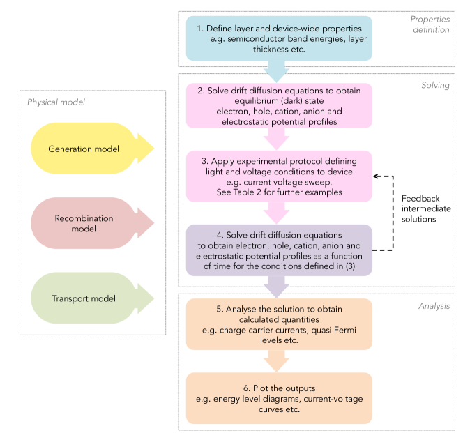
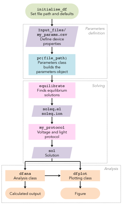
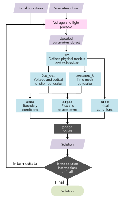
A flow diagram summarising Driftfusion’s general workflow is given in Figure 1. The system is designed such that the user performs a linear series of steps to obtain a solution; (1) the process begins with the creation of a semiconductor device object for which both device-wide properties, such as the carrier extraction coefficients, and layer-specific properties, such carrier mobilities are defined. A user-definable physical model comprised of one-dimensional generation, recombination and transport models determines the continuity equation for each charge carrier (see Section 3 for the default expressions); (2) the continuity equations are solved simultaneously with Poisson’s equation (Equation 17) to obtain a solution for the electron density, hole density, cation density (optional), anion density (optional), and electrostatic potential distributions at equilibrium; (3) an experimental protocol such as a current-voltage scan is defined using the appropriate input parameters e.g. scan rate and voltage limits. The protocol generates time-dependent voltage and light conditions that are subsequently applied to the device, typically using the equilibrium solution as the initial conditions. In more sophisticated protocols the solution is broken into a series of steps whereby intermediate solutions are fed back into the solver. Likewise, protocols can be cascaded such that the solution from one protocol supplies the initial conditions for the next; (4) the desired solution is output as a MATLAB data structure (see Solution structures highlighted box); (5) the solution structure can be analysed to obtain calculated outputs such as the charge carrier currents, quasi-Fermi levels etc; (6) a multitude of plotting tools are available to visualise the simulation outputs. Instructions on how to run each step programmatically and further details of the system architecture, protocols, solutions, and analysis functions are given in Section 4.
2.2 Licensing information
The front end code of Driftfusion has been made open-source under the GNU Affero General Public License v3.0 in order to accelerate the rate of development and expand our collective knowledge of mixed ionic-electronic conducting devices.Calado2017 It is important to note, however, that Driftfusion currently uses MATLAB’s Partial Differential Equation solver for Parabolic and Elliptic equations (pdepe), licensed under the MathWorks, Inc. Software License Agreement, which strictly prohibits modification and distribution. If you use Driftfusion please consider giving back to the project by providing feedback and/or contributing to its continued development and dissemination.
We now proceed to describe the default physical models underlying this release of Driftfusion.Calado2017 Herein relevant Driftfusion functions and commands are highlighted using boxes and referred to using command line typeface.
3 Implementation of established semiconductor theoretical principles in Driftfusion
The device physics implemented in Driftfusion is principally based on established semi-classical semiconductor transport and continuity principles, which are well described in Sze & KwokSze1981 and NelsonNelson2003 . Elements of this section are adapted from Ref. calado2017transient and are provided here as a direct reference for the reader. The equations described herein are written in terms of a single spatial dimension and can only be applied to devices with one-dimensional architectures and for which the material layers are homogeneous.
Driftfusion evolved from a diffusion-only code written to simulate transient processes in dye sensitised solar cellsBarnes2011 and uses MATLAB’sMATLAB2017 built-in pdepe solver.pdepe2013 The code solves the continuity equations and Poisson’s equation for electron density , hole density , cation density (optional), anion density (optional), and the electrostatic potential as a function of position , and time .
The full details of the numerical methods employed by the pdepe solver for discretising the equations are given in Skeel & Berlizns 1990.Skeel1990
3.1 Semiconductor energy levels
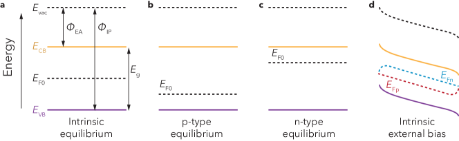
Figure 2a shows the energy levels associated with an idealised intrinsic semiconductor. The electron affinity and ionisation potential are the energies required to add an electron to the conduction band (CB) from the vacuum level and to remove an electron from the valence band (VB) to respectively. Note that in contrast to the established convention and the description given here, in Driftfusion and are input as negative values for consistency with other energetic properties referenced using the electron energy scale.
The electronic band gap of the material can be defined as:
| (1) |
3.1.1 The vacuum energy
The vacuum energy, is defined as the energy at which an electron is free of all forces from a solid including atomic and external potentials.Nelson2003 Spatial changes in the electrostatic potential, are therefore reflected in such that, at any point in space,
| (2) |
where is the elementary charge.
3.1.2 Conduction and valence band energies
The conduction and valence band energies and are defined as the difference between the vacuum energy and and respectively.
| (3) |
| (4) |
The band energies then, include both the potential energy associated with the specific molecular orbitals of the solid and the electrostatic potential arising from the existence of charge both within and external to the material.
3.2 Electronic carrier densities and quasi-Fermi levels
3.2.1 The occupation probability distribution function and electronic equilibrium carrier densities
At equilibrium the net exchange of mass and energy into and out of, as well as between different locations within a system is zero. Under these conditions the average probability, that an electron will occupy a particular state of energy, at equilibrium in a semiconductor at temperature is given by the Fermi-Dirac (F-D) distribution function:
| (5) |
where is Boltzmann’s constant. The equilibrium Fermi energy defines the energy at which a hypothetical electronic state has a % probability of occupation. At equilibrium, and for , the Fermi energy is identical to the chemical potential of the material. For an intrinsic semiconductor, lies close to the middle of the gap. Where the semiconductor is p-type, dopant atoms accept electrons from the bands, shifting towards the valence band (Figure 2b). Similarly, where the semiconductor is n-type, dopants donate electrons to the bands, shifting towards the conduction band (Figure 2c). Note that herein the subscript ‘’ denotes the value or expression of properties at equilibrium e.g. is the conduction band energy at equilibrium.222It follows that is only dependent on position, while is also time dependent due to the time-dependent nature of .
To obtain the density of free electrons in the conduction band, , the product of the probability distribution function, and the conduction band density of states (DOS) function, is integrated across energies above the conduction band edge, :
| (6) |
Similarly, to obtain the density of free holes in the valence band , the product of the average probability that an electron is not at energy (i.e. ) with the valence band DOS function, is integrated across all energies up to the valence band edge :
| (7) |
For semiconductor materials, and are typically modelled as parabolic functions with respect to electron energy at energies close to the band edges. Specifcally, and , where and are the effective electron and hole masses and is Planck’s constant. Unfortunately, closed-form solutions cannot be found to Equations 6 and 7 using the parabolic band approximation and the F-D distribution function (Equation 5). Hence, we use Blakemore’s approximationBlakemore1982 to the above integrals to obtain closed-form expressions for the equilibrium carrier densities:
| (8) |
| (9) |
where and are the temperature-dependent333For simplicity, the temperature-dependence of and has been omitted from the equations herein and it should further be noted that this temperature dependence is not explicitly dealt with in this release of Driftfusion. effective density of states (eDOS)444 and of the conduction and valence bands respectively. is a constant defining how close the approximation is to the Boltzmann regime (note that Equations 8 and 9 reduce to the Boltzmann approximation for ). Following Farrell et al., we set by default for ordered materials.Farrell2017a This results in a close agreement to F-D statistics for , such that degenerate semiconductor states are permissible within the scope of the model.
3.2.2 Equilibrium Fermi levels in doped materials
In charge-neutral n-type materials the equilibrium electron density is approximately equal to the density of donor dopant atoms such that . Similarly in p-type materials, , where is the density of acceptor dopants. In Driftfusion users input values for for each material layer and the corresponding equilibrium carrier and doping densities, , , , and are calculated during creation of the device parameters object (see Section 4.2) according to Equations 8 and 9.
3.2.3 Quasi-Fermi levels
A key approximation in semiconductor physics is the assumption that, under external optical or electrical bias, the electron and hole populations at any particular location can be treated separately, with individual distribution functions and associated quasi-Fermi levels (QFLs), and (Figure 2d). This is permitted because thermal relaxation of carriers to the band edges is typically significantly faster than interband relaxation, resulting in quasi-equilibrium states for each population.Nelson2003 Under these circumstances a similar approach to that taken for the true equilibrium state can be used to derive expressions for the QFLs:
| (10) |
| (11) |
It can be helpful to conceptualise the QFLs as the sum of the electrostatic () and average chemical potential energy ( for electrons, for holes) components of the carriers at each location. It follows that the gradient of the QFLs provides a convenient way to determine the direction of the current since, from the perspective of the electron energy scale, electrons move ‘downhill’, and holes move ‘uphill’ in response to electrochemical potential gradients. Moreover, the electron and hole currents, and , can be expressed in terms of the product of the electron and hole QFL gradients with the corresponding carrier conductivities, and :
| (12) |
| (13) |
Here, the conductivities are the product of the electronic carrier mobilities and with their corresponding concentrations and the elementary charge:
| (14) |
| (15) |
3.2.4 Open circuit voltage
The open circuit voltage, is the maximum energy per unit charge that can be extracted from an electrochemical cell for a given charge state at open circuit. The can be calculated using the difference in the electron QFL at the location of the cathode () and the hole QFL at the location of the anode () with the cell at open circuit.
| (16) |
3.3 Poisson’s equation
Poisson’s equation (Gauss’s Law) relates the electrostatic potential to the space charge density and the material dielectric constant via the Divergence Theorem. The space charge density is the sum of the mobile carrier and static charge densities at each spatial location. Doping is simulated via the inclusion of fixed charge density terms for ionising donor and acceptor atoms. In the default version of Driftfusion mobile ionic carriers are modelled as Schottky defectsWalsh2015 for which every ion has an oppositely charged counterpart, maintaining overall ionic defect charge neutrality within the device.555For clarity only charge neutrality of the Schottky defect terms is guaranteed, this does not include the contribution from dopant atoms, which may not be compensated by electronic carriers in regions where an electric field is present. The mobile cation density is initially balanced by a uniform static counter-ion density and the mobile anion density is similarly balanced by a static density . For the one-dimensional system described, Poisson’s equation can be explicitly stated as:
| (17) |
where is permittivity of free space. We emphasise that , , , and represent mobile species, while , , and are static ion densities. , and are the integer charge states for the ionic species (by default , and ).
3.4 Charge transport: Drift and diffusion
As the name suggests, the drift-diffusion (Poisson-Nernst-Planck) model assumes that charge transport within semiconductors is driven by two processes:
-
1.
Drift arising from the Lorentz force on charges due to an electric field , where .
-
2.
Diffusion arising from the entropic drive for carriers to move from regions of high to low concentration.
3.4.1 Bulk transport
Within the bulk of material layers the expressions for the flux density of electrons , holes , anions , and cations with mobility and diffusion coefficient (where denotes a generic charge carrier) are given by:
| (18) |
| (19) |
| (20) |
| (21) |
Figure LABEL:fig:Fluxes illustrates how the direction of electron and hole flux densities is determined from gradients in the electric potential and charge carrier densities. An analogous diagram can be drawn for mobile ionic species by substituting cations for holes and anions for electrons. The carrier (particle) currents are calculated as the product of the flux densities with the specific carrier charge such that .
3.4.2 Diffusion enhancement
The implementation of electronic carrier statistics beyond the Boltzmann approximation (Section 3.2.1) necessitates the inclusion of a generalised Einstein relation to define the relationship between the carrier mobilities and diffusion coefficients as a function of band state occupancy.Farrell2017a The result is a non-linear diffusion enhancement as the QFLs approach and move into the bands. Under Blakemore’s approximation,Blakemore1982 the diffusion coefficient-mobility relationships for electrons and holes can be expressed using the closed-forms:
| (22) |
| (23) |
We use similar expressions to those above for the ionic carriers from a model proposed by Kilic et al.Kilic2007 to account for steric effects at high ion densities:
| (24) |
| (25) |
Here and denote the limiting anion and cation densities. In the first instance these are set to the lattice cite density for the corresponding ions.
3.4.3 Transport across heterojunctions
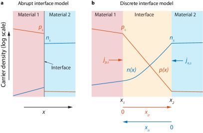
At the interface between two different semiconductor materials there is a change in the band energies and electronic density of states. In Driftfusion we choose to model the mixing of states at the interface using a smooth transition in material properties over a discrete interlayer region, in contrast to the commonly employed abrupt interface model777We note that while either model may be closer in one or more aspects to the real situation, both lack a comprehensive quantum mechanical treatment. (see Figure 4 below for a schematic illustrating the difference between the two models). To accommodate this approach, Equations 18 and 19 are modified to include additional gradient terms for spatial changes in , , , and . This leads to an adapted set of flux equations for electrons and holes within the interfaces:Zeman2011
| (26) |
| (27) |
Values of between nm have been extensively tested for the interfacial region thickness and are used in the example parameter files accompanying Driftfusion. By default, and are graded linearly, while and are graded exponentially within the interfacial regions.
3.4.4 Displacement current
The displacement current , as established in the Maxwell-Ampere law, is the rate of change of the electric displacement field, . In terms of the electric field the displacement current can be expressed as:
| (28) |
3.4.5 Total current
The total current, is the sum of the individual current components at each point in space and time:
| (29) |
3.4.6 Validity criteria for the drift-diffusion equations
The drift-diffusion approach set out above is valid for semiconductor materials that satisfy the following criteria:Nelson2003
-
1.
The electron and hole populations are at quasi-thermal equilibrium.
-
2.
The electron and hole population temperatures are the same as that of the lattice.
-
3.
Changes in state occupancy are more likely to be due to scattering collisions within a band than generation and recombination events between bands or trapping events.
-
4.
The electron and hole states can be described by a quantum number, .
-
5.
The mean free path length of carriers, is significantly shorter than the layer thickness, ().
3.5 Charge continuity
The continuity equations are a set of ‘book-keeping’ equations, based on the conservation of charge, describing how charge carrier densities change in time at each location. In one-dimension, the continuity equation for a generic carrier density with flux density , and source/sink term can be expressed as:
| (30) |
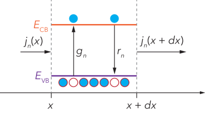
For electronic carriers is composed of two components; 1. Generation, of carriers by both thermal and photo excitation and; 2. Recombination, of carriers through radiative (photon emission) and non-radiative pathways. Figure 3 illustrates the principle of continuity: changes in the electron concentration with time within a thin slab are determined by the generation, recombination, and difference between the incoming and outgoing flux density of carriers.
Where chemical reactions take place within devices, additional generation and recombination terms for carriers may also contribute to . In the current version of Driftfusion, mobile ionic charge carriers are treated as inert such that . Users are, however, free to edit the default source terms using the Equation Editor (Section 4.5). A guide describing how to do this is included in the Supplemental Information Section LABEL:sec:edit_equations.
In one-dimension the continuity equations for electrons, holes, cations and anions are given by:
| (31) |
| (32) |
| (33) |
| (34) |
3.5.1 Steady-state approximation to electronic carrier densities and fluxes within the interfacial regions
To better understand the discrete interface model employed by Driftfusion we solve the electron and hole continuity equations (Equations 26, 27, 31 and 32) to obtain analytical expressions for the electronic carrier densities within the discrete interfacial regions using the following approximations and assumptions:
-
1.
Carriers within an interface are at steady-state with respect to the surroundings layers (, ).
-
2.
There is no optical generation within the interface ().
-
3.
The electric field can be treated as approximately constant throughout the interfacial region ().
-
4.
The recombination rate, within the interfacial region is constant and distributed uniformly.
-
5.
QFLs remain within the Boltzmann regime ( and )
As detailed in the Supplemental Information Section LABEL:sec:ss_carriers_interfaces, using the boundary conditions , , , and (see Figure 4b), the following expressions can be obtained for the carrier densities within the interfacial regions:
| (35) |
| (36) |
where,
| (37) |
| (38) |
The corresponding fluxes are given by:
| (39) |
| (40) |
As illustrated in Figure 4b, the translated co-ordinates and are taken to be in the direction for which and are negative and typically the direction for which carrier densities decay.
Example solutions comparing the analytical approximations to numerical solutions calculated using Driftfusion under different transport and recombination regimes are given in the Supplemental Information, Section LABEL:sec:interface_ana_validation. Where transport is a limiting factor within the interfaces the solutions become strongly dependent on the boundary flux and recombination rates. It is noteworthy however that in the limiting case of infinitely fast transport () Equations 35 and 36 converge towards purely exponential forms for which the carrier densities change by a Boltzmann factor ( and ) across the width of the interface, . For the special case where , the result is a change in carrier densities equivalent to that expected from an abrupt interface model using Boltzmann statistics. The results presented in this section are applied below in Section 3.7.3 to the interfacial volumetric surface recombination model.
3.6 Electronic carrier generation
Two optical models for electronic carrier generation are currently available for use in Driftfusion; uniform generation for which a uniform volumetric generation rate, is defined for each layer (excluding interfacial regions) and; Beer-Lambert law generation as described below. Irrespective of the choice of optical model the generation rate is zeroed within the interfacial regions to avoid potential stability issues.
3.6.1 Beer-Lambert law generation
The Beer-Lambert law models the photon flux density as falling exponentially within a material with a characteristic photon energy-dependent absorption coefficient . The volumetric generation rate , over a range of photon energies with incident photon flux density , is given by the integral across the spectrum:
| (41) |
where is the reflectance. For simplicity, we assume that a single electron-hole pair is generated by a single photon.
3.6.2 Arbitrary generation profiles
An arbitrary generation profile can be inserted following creation of the parameters object for users who wish to use profiles calculated from different models using an external software package. Details on how to do this are given in Section 4.2.7.
3.7 Recombination
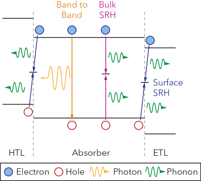
By default, two established models for recombination are included in Driftfusion: band-to-band recombination and trap-mediated Shockley-Read-Hall (SRH) recombination. Figure 5 is a simplified energy level schematic illustrating these mechanisms. The recombination expressions can be modified in the source terms of the Equation Editor (Section 4.5).
3.7.1 Band-to-band recombination
The rate of band-to-band recombination (also commonly termed direct, radiative or bimolecular recombination) is proportional to the product of the electron and hole densities at a given location such that:
| (42) |
where is the band-to-band recombination rate coefficient. The term is equivalent to including an expression for thermal generation and ensures that at steady-state.
3.7.2 Shockley-Read-Hall (SRH) recombination
Recombination via trap states is modelled using a simplified Shockley-Read-Hall (SRH) recombinationShockley1952 expression for which the capture cross section, mean thermal velocity of carriers, and trap density are collected into SRH time constants, and for electrons and holes respectively:
| (43) |
Here, and are parameters that define the dependence of the recombination rate to the trap level and are given by the electron and hole densities when their respective QFLs are at the position of the trap energy, :
| (44) |
| (45) |
It should be noted that Equation 43 is valid only when trapped carriers are in thermal equilibrium with those in the bands. It follows that the rate of trapping and de-trapping of carriers is assumed to be fast compared to the timescale being simulated, such that the approximation is reasonable. In the current version of Driftfusion we also assume that the quantity of trapped carriers is negligible compared to that of the free carriers such that trapped carriers can be neglected in Poisson’s equation. To more completely simulate the dynamics of capture and emission of carriers, and the associated contribution to the chemical capacitance of devices, one or more additional variables could be included.
3.7.3 Surface recombination at interfaces
Abrupt interface models typically use a SRH surface recombination model to determine the recombination flux, between majority carriers and at the interface between two materials (see Figure 4a):Courtier2019a
| (46) |
Here, and are the surface recombination velocities for electrons and holes at the interface. This model implies that the electron and hole populations in the two materials have delocalised wave functions that overlap significantly such that recombination events are probable.
Since Driftfusion uses discrete interfacial regions, in order to obtain an equivalent recombination flux to the abrupt interface model, we convert Equation 46 into a volumetric surface recombination rate, by distributing the recombination uniformly across a zone of thickness, within the interface (see Figure LABEL:fig:rec_zone), such that . By default the recombination zone is automatically located next to the interface with the highest minority carrier density at equilibrium. To obtain an expression for , Equations 35 and 36 can be rearranged to express and in terms of and :
| (47) |
| (48) |
For sufficiently high values of , and the and terms dominate Equations 47 and 48 and the carrier density profiles within the interfaces tend towards purely exponential functions, such that and . In many instances it is then sufficient to approximate the volumetric surface recombination rate within the recombination zone as:
| (49) |
where and are given in Equations 37 and 38, and the term is subsumed into the volumetric surface recombination time constants, and such that:
| (50) |
| (51) |
We stress here that this is not a physically motivated model in the sense that we do not anticipate recombination to be distributed uniformly throughout a recombination zone in reality. This approach does however result in a good approximation to the established abrupt interface surface recombination model for a wide variety of devices and conditions (see Section 5.4).
3.8 Initial conditions
At present two sets of initial conditions are used in Driftfusion, dependent on the number of layers. These conditions are designed to be consistent with the boundary conditions and to minimise the error in the space charge density at junctions which can lead to large electric fields and convergence failure.
3.8.1 Single layer device
A linearly varying electrostatic potential and exponentially varying electronic carrier densities over the layer thickness are used as the initial conditions (Equations 53, 54, and 52) when simulating a single layer. Uniform ionic carrier density profiles are used throughout the layer to guarantee ionic defect charge neutrality (Equations 56 and 55).
| (52) |
| (53) |
| (54) |
| (55) |
| (56) |
Here, the built-in potential of the device is determined by the difference in boundary electrode workfunctions and :
| (57) |
3.8.2 Multilayer device
For multilayer devices the electrostatic potential is set to fall uniformly throughout the device (Equation 58), while the electronic carrier densities are chosen to be the equilibrium densities for the individual layers ( and ). As with the single layers, the ionic carriers are given a uniform density (Equations 59 - 61), thus guaranteeing local electro-neutrality.
| (58) |
| (59) |
| (60) |
| (61) |
| (62) |
Here, the device thickness is the sum of the individual layer thicknesses (). Driftfusion auto-detects the number of layers in the device and uses the appropriate set of initial conditions when running the equilibrate protocol to obtain the equilibrium solutions for the device (Section 4.3).
3.9 Boundary conditions
Solving Equation 17 and Equations 31 - 34 requires two constants of integration for each variable, which are provided by the system boundary conditions. For the charge carriers, Neumann (defined-flux value) conditions are used to set the flux density into and out of the system. The electrostatic potential uses Dirichlet conditions (defined-variable value) such that the potential is fixed at both boundaries at each point in time as detailed in Section 3.9.1. The details of these boundary conditions are discussed in the following subsections.
3.9.1 Electrostatic potential boundary conditions
In Driftfusion the electrostatic potential at the left-hand boundary is set to zero (Equation 63) and used as the reference potential. The applied electrical bias, and an effective potential arising from series resistance are applied to the right-hand boundary as described in Equation 64.
| (63) |
| (64) |
Here, Ohm’s law is used to calculate from the electron and hole flux densities:
| (65) |
where is the area-normalised series resistance, given by the product of the external series resistance and the device active area. Setting to a high value (e.g. cm2) approximates an open circuit condition for devices with metal electrodes. Technically this can be achieved using the lightonRs protocol (see Section 4.4 for a description of protocols).888Note that at the time of writing this method is not stable for all input parameter sets.
3.9.2 Carrier selectivity and surface recombination at the system boundaries
Many architectures of semiconductor device, including solar cells and LEDs employ selective contact layers that block minority carriers from being extracted (or injected) via energetic barriers. These are known variously as transport layers, blocking layers, blocking contacts, or selective contacts. For solar cells semiconductor layers are typically sandwiched between two metallic electrodes constituted of metals or highly-doped semiconductors. Such materials can be numerically challenging to simulate owing to their high charge carrier densities and thin depletion widths. Consequently, a common approach is to use boundary conditions defining charge carrier extraction and recombination flux densities to simulate the properties of either the contact or electrode material. It should be noted, however, that the employment of fixed electrostatic potential boundary conditions (as defined in Section 3.9.1) implies that the potential falls only within the discrete system and not within the electrodes. This approximation is only realistic for contact materials with vanishingly small depletion widths (infinite interfacial capacitances) i.e. metals and highly doped semiconductors. It follows that to accurately simulate semiconductor contacts layers with finite depletion regions these layers must also be included within the discretised system.
For electronic carriers the surface recombination velocity coefficients and determine the carrier extraction/recombination rate at the boundaries of the system. For majority carriers in solar cells, high values of and (e.g. cm s-1Tress2011 ) are advantageous for carrier extraction, while low values imply poor contact extraction properties. For minority carriers, high values of and are typically undesirable as they imply high rates of surface recombination at the electrode. In Driftfusion the expressions for electronic boundary carrier flux densities, and are given by the typical first-order expressions:
| (66) |
| (67) |
| (68) |
| (69) |
where , , , and are the equilibrium carrier densities at the left () and right-hand () boundaries, calculated using Equations 8 and 9 under the assumption that the semiconductor QFLs are at the same energy as the electrode Fermi energy, which is assumed to remain constant. For the left-hand boundary and are given by Equations 70 and 71.
| (70) |
| (71) |
where is the left-hand electrode work function. Analogous expressions are used for and at the right-hand boundary. Extraction barriers can also be modelled with this approach by including a term for the barrier energy in the exponent of Equations 70 and 71. At present, however, quantum mechanical tunnelling and image charge density models for energetic barriers at the system boundaries are not accounted for in Driftfusion.
3.9.3 Ionic carrier boundary conditions
In the simplest case, ionic carriers are confined to the device and do not react at the electrode boundaries. This leads to a set of zero flux density boundary conditions for mobile anions and cations:
| (72) |
| (73) |
| (74) |
| (75) |
Where an infinite reservoir of ions exists at a system boundary (such as an electrolyte), a Dirichlet boundary condition defining a constant ion density could alternatively be imposed.
This concludes our description of the physical models employed in Driftfusion. In the following section the system architecture and key commands are introduced as well as a guide on how to get started with using Driftfusion.
4 System architecture and how to use Driftfusion
Driftfusion is designed such that the user performs a linear sequence of simple procedures to obtain a solution. The key steps are summarised in Figure 6; Following initialisation of the system, the user defines a device by creating a parameters object containing all the individual layer and device-wide properties; The equilibrium solutions (soleq.el and soleq.ion) for the device are then obtained before applying a voltage and light protocol, which may involve intermediate solutions; Once a desired solution (sol) has been obtained, analysis and plotting functions can be called to calculate outputs and visualise the solutions. Below, the principal functions are discussed in further detail.
4.1 Initialising the system: initialisedf
At the start of each MATLAB session, initialisedf needs to be called from within the Driftfusion parent folder (not one of its subfolders) to add the program folders to the file path and set plotting defaults. This action must be completed before any saved data objects are loaded into the MATLAB workspace to ensure that objects are associated with their corresponding class definitions.
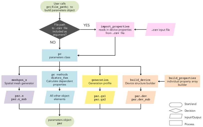
4.2 Defining device properties and creating a parameters object: pc(filepath)
The parameters class, pc contains the default device properties and functions required to build a parameters object, which we shall denote herein as par. The parameters object defines both layer-specific and device-wide properties. Layer-specific properties must be a cell or numerical array containing the same number of elements as there are layers, including interface layers. For example, a three-layer device with two heterojunctions requires layer-specific property arrays to have five elements. Examples can be found in the /Input_ files folder (see Section 4.2.1).
Figure 7 shows the processes through which the main components of the parameters object are built; The user is required to define a set of material properties for each layer. The comments in pc describe each of the parameters in detail and give their units (also see Supplemental Information, Table LABEL:tbl:symbols for quick reference); Several subfunctions (methods) of pc then calculate dependent properties, such as the equilibrium carrier densities for example, from the choice of probability distribution function (probdistrofunction) and other user-defined properties. The treatment of properties in the device interfaces is dealt with, and can be changed, using the device builder builddevice (see below).
4.2.1 Importing properties
Typically, the most important user-definable properties are stored in a .csv file, which is easily editable with a spreadsheet editor such as LibreOffice or Microsoft Excel. The file path to the .csv file can then be used as an input argument for pc, for example:
This allows the user to easily create and store sets of key device parameters without editing pc. Default values for properties set in the parameters class pc will be overwritten by the values in the .csv file during creation of the parameters object par. New properties defined in pc can easily be added to the .csv file provided that they are also included in importproperties, which tests to see which properties are present in the text file and reads them into the parameters object where present. Following the properties read-in step performed by importproperties, the number of rows in the layertype column (see Section 4.2.2) is used for error checking all other entries to confirm that properties have been defined for each discrete layer of the system (this does not include the electrode rows, which are pseudo-layers). To avoid potential incompatibility, new user-defined material properties defined in pc, which have distinct values for each layer, should be included in the .csv file and added to the list of importable properties in importproperties, as well as builddevice. An example of how to do this is given in the Supplemental Information, Section LABEL:sec:edit_equations.
| Column heading | Description | Options/range | Units | Section ref. |
|---|---|---|---|---|
| layertype | Layer type | electrode, layer, active, interface | - | 4.2.2 |
| material | Chemical short-form name | Materials contained within ./Libraries/IndexofRefractionlibrary.xls | - | 4.2.7 |
| thickness | Layer thickness | cm | 4.2.3 | |
| layerpoints | Number of points in the layer | - | 4.2.3 | |
| xmeshceoff | A parameter defining how densely the spatial mesh points are concentrated at the boundaries of the layer for xmeshtype = ‘erf-linear’ | norm. | 4.2.3 | |
| PhiEA | Electron affinity1 | - | eV | 3.1 |
| PhiIP | Ionisation potential1 | - | eV | 3.1 |
| EF0 | Equilibrium Fermi energy2,3 | PhiIP, PhiEA | eV | 3.2.1 |
| Et | SRH trap energy level (single trap level model) | PhiIP, PhiEA | eV | 3.7, 3.7.3 |
| Nc | Effective density of conduction band states | - | cm-3 | 3.2.1 |
| Nv | Effective density of valence band states | - | cm-3 | 3.2.1 |
| Ncat | Intrinsic Schottky defect density (mobile cations) at equilibrium | cmax | cm-3 | 3.3 |
| Nani | Intrinsic Schottky defect density (mobile anions) at equilibrium | amax | cm-3 | 3.3 |
| cmax | Limiting mobile cation density | Ncat | cm-3 | 3.4.2 |
| amax | Limiting mobile anion density | Nani | cm-3 | 3.4.2 |
| mun | Electron mobility | cm2 V-1 s-1 | 3.4 | |
| mup | Hole mobility | cm2 V-1 s-1 | 3.4 | |
| muc | Cation mobility | cm2 V-1 s-1 | 3.4 | |
| mua | Anion mobility | cm2 V-1 s-1 | 3.4 | |
| epp | Relative dielectric constant | - | 3.3 | |
| g0 | Uniform generation rate | cm-3 s-1 | 3.6, 4.2.7 | |
| B | Band-to-band recombination rate coefficient | cm-3 s-1 | 3.7.1 | |
| taun | SRH electron lifetime | s | 3.7.2 | |
| taup | SRH hole lifetime | s | 3.7.2 | |
| sn | Electron surface recombination velocity2,4 | cm s-1 | 3.7.3, 3.9 | |
| sp | Hole surface recombination velocity2,4 | cm s-1 | 3.7.3, 3.9 | |
| vsrzoneloc | Volumetric interfacial surface recombination zone location | auto, L, C, R | - | 3.7.3 |
| Red | Layer colour red RGB triplet component | norm. | - | |
| Green | Layer colour green RGB triplet component | norm. | - | |
| Blue | Layer colour blue RGB triplet component | norm. | - | |
| opticalmodel | Optical model | uniform, Beer-Lambert | - | 3.6,4.2.7,3.6.1 |
| xmeshtype | Spatial mesh type | linear, erf-linear | - | 4.2.3 |
| side | Illumination side | left, right | - | - |
| Nionicspecies | Number of mobile ionic species | (cations), (cations & anions) | - | - |
4.2.2 Layer types
Layer types, set using the layertype property, flag how each layer should be treated. Driftfusion currently uses three layer types:
-
1.
‘electrode’: A pseudo-layer which defines the boundary properties of the system. These are not discrete layers and do not appear in visualised outputs.
-
2.
‘layer’: A slab of semiconductor for which all properties are spatially constant.
-
3.
‘active’: As layer but flags the active layer of the device. The number of the first layer designated ‘active’ is stored in the activelayer property and is used for calculating further properties such as the active layer thickness, dactive. Flagging the active layer proves particularly useful when automating parameter explorations as the active layer can easily be indexed.
-
4.
‘interface’: An interfacial region between two different material layers. The properties of the interface are varied according to the specific choice of grading method as defined in builddevice (see below). It is critical that interfacial layers are included between material layers with different energy levels and eDOS values i.e. at heterojunctions. See the included default input files for examples of how to set up devices with heterojunctions.
4.2.3 Spatial mesh
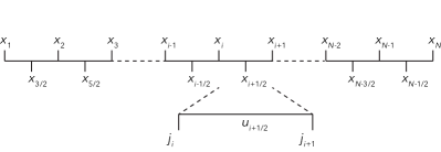
The computational grid is divided into intervals with subintervals, where the position of the subintervals is defined by for . pdepe solves for the variable values on the subintervals () and their associated flux densities on the integer intervals () as illustrated in Figure 8.
Owing to the use of a finite element discretisation scheme the details of the spatial mesh in Driftfusion are of critical importance to ensure fast and reliable convergence. In this release of Driftfusion two types of spatial mesh are available:
-
1.
‘linear’: Linear piece-wise spacing
-
2.
‘erf-linear’: Mixed error function (bulk regions)- linear (interfacial regions) piece-wise spacing
meshgenx generates integer and subinterval spatial meshes, x and xsub respectively (see Figure 8), based on the layer thickness, the number of layerpoints defined in the device properties, and the xmeshtype. The solution is interpolated for the integer grid points when generating the output solution matrix sol.u (see Section 4.6). The property xmeshcoeff controls the spread of points for regions where an error function is used for point spacing i.e. layer and active layer types: higher values determine higher point densities close to the layer boundaries. In general we recommend using ‘erf-linear’ for devices with relatively high ionic defect densities as, where ionic carriers are confined, high point densities are required at the layer boundaries to resolve the carrier distributions. Where the depletion of ionic carriers extends into the bulk xmeshceoff can be reduced to increase the bulk point density.
4.2.4 Time mesh
pdepe uses an adaptive time step for forward time integration and solution output is interpolated for the user-defined time mesh. Convergence of the solver is weakly-dependent of the user-defined time mesh interval spacing and strongly-dependent on the maximum time and the maximum time step. These can be adjusted by changing the tmax and MaxStepFactor properties of the parameters object (see Section 4.2). The options for different time mesh types (tmeshtype) are:
-
1.
‘linear’ or 1
-
2.
‘’ or 2
Typically, the time mesh is changed frequently for intermediate solutions within protocols to accommodate the different timescales on which carriers move. For example, in some cases the ionic carriers may be frozen to obtain a stable short timescale solution for the electronic carriers, before a second, longer timescale, solution is calculated with the ionic carriers mobile. Similarly the tmeshtype is adjusted dependent on the voltage and light conditions. For example during a scan a linear time mesh is used in keeping with the linear change in the applied voltage with time. In other instances a logarithmic mesh is more appropriate in order to resolve time periods for which the carrier time derivatives are larger.
4.2.5 The device structures
builddevice and buildproperty are called during creation of the parameters object to build two important data structures, which we call the ‘device structures’: dev, defined on the integer grid intervals (), is used to determine the initial conditions only, while devsub, defined on the subintervals (), is used by the pdepe solver function. dev and devsub contain arrays defining all spatially varying properties at every location within the device including the interfacial regions. buildproperty enables the user to specify different types of interface grading for each property listed in builddevice. At present there are four generic grading option types:
-
1.
‘zeroed’: The value of the property is set to zero throughout the interfacial region.
-
2.
‘constant’: The value of the property is set to be constant throughout the interfacial region. Note that the user must define this value in the .csv file.
-
3.
‘lin_ graded’: The property is linearly graded using the property values of the adjoining layers.
-
4.
‘exp_ graded’: The property is exponentially graded using the property values of the adjoining layers.
For the volumetric surface recombination scheme described in Section 3.7.3, we also introduce parameter-specific grading schemes for the VSR time constants:
The interface grading type for each property is set in the builddevice function e.g. the default grading type for the electron affinity, is ‘lin_ graded’.
Dependent on the choice of grading option, input values may, or may not, be required for a given material property in the interfacial layers. For example, when using the ‘lin_ graded’ option a value is not needed because the interface property values are calculated from those of the adjacent layers. By contrast, when using the ‘constant’ option, a property value does need to be specified for the interfacial layer to avoid an error. Since property values that are not required are ignored, we recommend that users specify all property values for all layers to future-proof against problems arising when experimenting with grading options.
4.2.6 The electronic carrier probability distribution function
The class distro_ fun defines the electronic carrier probability distribution function for the model and calculates equilibrium boundary, and initial carrier densities when building the parameters object. At present there are two available options for the choice of probability distribution function:
-
1.
‘Boltz’ - The Boltzmann approximation ()
-
2.
‘Blakemore’ - The Blakemore approximation ( see Section 3.2.1)
While the Boltzmann approximation results in marginally faster calculations owing to the absence of a diffusion enhancement we recommend using Blakemore statistics for their extended domain of validity.
4.2.7 The electronic carrier generation profile function
generation calculates the two generation profiles gx1 and gx2, which can be used for a constant bias light and a pulse source for example, at each spatial location in the device for the chosen opticalmodel and light sources (see Section 3.6 and the flow diagram in the Supplemental Information Figure LABEL:fig:generation_flow). The light sources can be set using the light_ source1 and light_ source2 properties. There are two options for the opticalmodel:
-
1.
‘uniform’: a uniform volumetric generation rate defined by the property g0 is applied layers with layer and active layer types. The multiplier properties int1 and int2 define the intensities for light source and respectively.
-
2.
‘Beer_ Lambert’: The generation profile follows the Beer-Lambert law as detailed in Section 3.6.1 with material layer optical properties taken from ./Libraries/IndexofRefraction_ library.xls for the corresponding materials defined in the par.material cell array. As with uniform generation, the generation rate profile is multiplied by the intensity properties int1 and int2 before being applied.
A arbitrary generation profile calculated using an external program (such as SolcoreAlonso-Alvarez2018a or the McGeeHee Group’s Transfer Matrix codeBurkhard2010 ) can be inserted into the parameters object par by overwriting the generation profile properties gx1 or gx2 following creation of the object. The profile must be interpolated for the subinterval () grid points defined by x_ sub (see Section 4.2.3). We also recommend that the generation rate is set to zero within the interfacial regions to avoid stability issues.
The light source time-dependencies are controlled using the g1_ fun_ type and g2_ fun_ type properties, which define the function type (e.g. sine wave) and the g1_ fun_ arg and g2_ fun_ arg properties, which are coefficient arrays for the function generator (see Section 4.5.5) e.g. the frequency, amplitude, etc.
4.3 Protocols: equilibrate
Once a device has been created and stored in the MATLAB workspace as a parameters object the next step is to find the equilibrium solution for the device. The function equilibrate starts with the initial conditions described in Section 3.8 and runs through a number of steps to find the equilibrium solutions, with and without mobile ionic carriers, for the device described by par. The output structure soleq contains two solutions (see Section 4.6);
-
1.
soleq.el: only the electronic charge carriers are mobile and are at equilibrium.
-
2.
soleq.ion: electronic and ionic carriers are mobile and are at equilibrium.
Storing both solutions in this way allows devices with and without mobile ionic charge to be compared easily.
4.4 Protocols: General
A Driftfusion protocol is defined as a function that contains a series of instructions that takes an input solution (initial conditions) and produces an output solution. For many of the existing protocols, listed in Table 2, with the exception of equilibrate, the input is one of the equilibrium solutions, soleq.el or soleq.ion. Figure 9 is a flow diagram illustrating the key functions called during execution of a protocol.
Protocols typically start by creating a temporary parameters object that is a duplicate of the input solution parameters object. This temporary object can then be used to write new voltage and light parameters that will be used by the function generator to define the generation rate at each point in space and time and the potential at the boundary at each point in time. Additional parameters, for example those defining the output time mesh or carrier transport are also frequently adjusted. The approach is to split a complex experimental protocol into a series of intermediate steps that facilitate convergence of the solver. For example, where ionic mobilities are separated by many orders of magnitude from electronic mobilities, a steady-state solution is easiest found by accelerating the ions to similar values to the electronic carriers using the K_ a and K_ c properties. The simulation can then be run with an appropriate time step and checked to confirm that a steady-state has been reached. The possibilities are too numerous to list here and users are encouraged to investigate the existing protocols listed in Table 2 in preparation of writing their own.
| Command | Description |
|---|---|
| changeLight | Switches light intensity using incremental intensity steps. |
| doCV | Cyclic Voltammogram (CV) simulation using triangle wave function generator . |
| doIMPS | Intensity Modulated Photocurrent Spectroscopy (IMPS) simulation at a specified frequency and light intensities. |
| doIMVS | Switches to open circuit (OC), runs to steady-state OC, then performs Intensity Modulated Photovoltage Spectroscopy (IMVS) measurement simulation at a specified frequency and light intensities. |
| doJV | Forward and reverse current-voltage (JV) scan with options for dark and constant illumination conditions. |
| doLightPulse | Uses light source 2 with square wave generator superimposed on light source 1 (determined by the initial conditions) to optically pulse the device. |
| doSDP | Step, Dwell, Probe (SDP) measurement protocol: Jump to an applied potential, remain at the applied potential for a specified dwell time and then perform optically pulsed current transient. See Ref. Belisle2016 for further details of the experimental protocol. |
| doSPV | Surface PhotoVoltage (SPV) simulation: Switches light on with high series resistance. |
| doTPV | Transient PhotoVoltage (TPV) simulation: Switches to open circuit with bias light and optically pulses the device. |
| equilibrate | Start from base initial conditions and find equilibrium solutions without mobile ionic charge (soleq.el) and with mobile ionic charge (soleq.ion). |
| findVoc | Obtains steady-state open circuit condition using Newton-Rhaphson minimisation. |
| findVocDirect | Obtains an approximate steady-state open circuit condition using 1 M cm2 series resistance. |
| genIntStructs | Generates solutions at various light intensities. |
| genIntStructsRealVoc | Generates open circuit solutions at various light intensities. |
| genVappStructs | Generates solutions at various applied voltages. |
| jumptoV | Jumps to a new applied voltage and stabilises the cell at the new voltage for a user-defined time period. |
| lightonRs | Switches on the light for a specified period of time with a user-defined series resistance. |
| stabilize | Runs a set of initial conditions to a steady-state. |
| sweepLight | Linear sweep of the light intensity over a user-defined time period. |
| transient_ nid | Simulates a transient ideality factor () measurement protocol.Calado2019_ideality |
| VappFunction | Applies a user-defined voltage function to a set of initial conditions. |
4.5 The Driftfusion master function df
df is the core of Driftfusion. The function takes the device parameters, and voltage and light conditions, calls the solver and outputs the solution (Figure 9). The underlying equations in Driftfusion can be customised for specific models and applications using the Equation Editor in the dfpde subfunction. df contains three important subfunctions: dfpde, dfic, and dfbc which we now proceed to describe.
4.5.1 Driftfusion Partial Differential Equation function dfpde and the Equation Editor
dfpde defines the equations to be solved by MATLAB’s Partial Differential Equation: Parabolic and Elliptic solver toolbox (pdepe).pdepe2013 For one-dimensional Cartesian co-ordinates, pdepe solves equations of the form:
| (76) |
Here, is a vector containing the variables , , , , and at each position in space and time . is a vector defining the prefactor for the time derivative, is a vector determining the flux density terms (note: does not denote the electric field in this section), and is a vector containing the source/sink terms for the components of . By default for charge carriers but could, for example, be used to change the active volume fraction of a layer in a mesoporous structure. The equations can be easily reviewed and edited in the dfpde Equation Editor as shown in Listing 1. Here, device properties that have a spatial dependence are indexed with the variable to obtain the corresponding value at the location given by x_ sub(i). A step-by-step example of how to change the physical model using the Equation Editor is given in the Supplemental Information, Section LABEL:sec:edit_equations.
4.5.2 Driftfusion Initial Conditions dfic
dfic defines the initial conditions to be used by pedpe. If running equilibrate to obtain the equilibrium solution or running df with an empty input solution, the first set of initial conditions are as described in Section 3.8. Otherwise, the final time point of the input solution is used.
4.5.3 Driftfusion Boundary Conditions dfbc
dfbc defines the system boundary conditions. The boundary condition expressions are passed to pdepe using two coefficients and , with elements, where is the number of independent variables being solved for. The boundary conditions are expressed in the form:
| (77) |
For Dirichlet conditions must be non-zero to define the variable values, whereas for Neumann conditions must be non-zero to define the flux density. Listing 2 shows how the default Driftfusion boundary conditions (described in Section 3.9) are implemented in the current version of the code.
In addition to these subfunctions, df also calls two important external functions: the time mesh generator, meshgen_ t and the function generator, fun_ gen.
4.5.4 The time mesh generator meshgen_ t.
df calls the time mesh generator meshgen_ t at the start of the code. As discussed in Section 4.2.4, the solver uses an adaptive time step and interpolates the solution to the user-defined mesh. Hence the choice of mesh is not critical to time integration convergence. The values of the mesh should be chosen such as to resolve the solution properly on the appropriate timescales. The total time step of the solution tmax and the maximum time step (controlled using the MaxStepFactor property) do however influence convergence strongly. For this reason, where convergence is proving problematic it is recommended that either tmax or MaxStepFactor is reduced and the solution obtained in multiple stages.
4.5.5 The function generator fun_ gen.
df calls fun_ gen to generate time-dependent algebraic functions that define the applied voltage and light intensity conditions. df includes the ability to call two different light intensity functions with different light sources, enabling users to simulate a constant bias light and additional pump pulse using the square wave generator for example. Each function type requires a coefficients array with a number of elements determined by the function type and detailed in the comments of fun_ gen. Listing 3 is an example from the ./Scripts/Vapp_ function_ script script showing how to define a sine wave function for the applied voltage:
4.6 Solution structures
df outputs a solution structure sol with the following components:
-
•
The solution matrix u: This is a three dimensional matrix for which the dimensions are (time, space, variable). The order of the variables are as follows:
-
1.
Electrostatic potential
-
2.
Electron density
-
3.
Hole density
-
4.
Cation density (where 1 mobile ionic carrier is stipulated)
-
5.
Anion density (where 2 mobile ionic carriers are stipulated)
-
1.
-
•
The spatial mesh x.
-
•
The time mesh t.
-
•
The parameters object par.
All other outputs can be calculated from the above by calling methods from dfana.
4.7 Calculating outputs: dfana
dfana is a collection of functions (methods) that enable the user to calculate outputs such as carrier currents, quasi-Fermi levels, recombination rates etc. from the solution matrix u, the parameters object par and the specified physical models. The use of a class in this instance enables the package syntax dfana.my_ calculation(sol) to be used. For example the command:
outputs a two dimensional matrix containing the space charge density as function of time and position. Many other examples of how dfana methods can be used to calculate outputs are given in the highlighted boxes of Section 3. The full list of the available analysis methods can be viewed and easily navigated by selecting the dfana.m in the Current Folder window and opening the functions browser sub-window.
4.8 Plotting the output: dfplot
dfplot is a class containing a collection of plotting methods. Similar to dfana, this enables the package syntax dfplot.my_ plot(sol) to be used. For variables plotted as a function of position, an optional vector argument can be included to plot the solution at , where is the time point to be plotted. For example the command:
plots the electrostatic potential component of the solution as a function of position at , , , , and s (an example is shown below in Figure 15a). If no second argument is given then only the final time point is plotted. dfplot also includes the generic property plotting function dfplot.x2d to allow users to easily create new two-dimensional plots.
For variables plotted as a function of time the second argument defines the position. For example the command:
plots the current density for each carrier as a function of position at cm. For plots where variables are integrated over a region of space, the second argument is a vector containing the limits . Further details can be found in the comments of dfplot.
4.9 Getting started and the example scripts
While the underlying system may appear complex, Driftfusion has been designed such that with a few simple commands, users can simulate complex devices and transient optoelectronic experiment protocols. Table 2 is a complete list of protocols available at the time of writing. In addition to the brief guide below, a quick start with up-to-date instructions can be found in the README.md file in the Driftfusion GitHub repository,Calado2017 and a series of example scripts for running specific protocols are also presented in the Scripts folder. New users are advised to study these scripts and adapt them to their own purposes. In addition, we have written an introductory workshop to guide students through the process of building basic semiconductor devices and applying optical and voltage biases to them. This can be found in the Getting-started-workshop-2021 branch of the Driftfusion GitHub repository.
4.9.1 How to build a device object, find the equilibrium solution and run a cyclic voltammogram
In this section some commonly-used commands are put together to show new users how to create a device object, obtain the device equilibrium solutions, and run a protocol, which in this example simulates a cyclic voltammogram (CV). The doCV protocol applies a triangular wave voltage function to the device, with optional constant illumination, for a set number of cycles enabling the device current-voltage characteristics at a given scan rate to be calculated.
At the start of each session, the system must be initialised by typing the command:
To create a parameters object using the default parameters for a Spiro-OMeTAD/perovskite/TiO2 perovskite solar cell the parameters class, pc is called with the file path to the appropriate .csv file as the input argument:
The equilibrium solutions with and without mobile ionic carriers for the device can now be obtained by calling the equilibrate protocol:
As discussed in Section 4.3, the output structure soleq contains two solutions: soleq.el and soleq.ion. In this example we are interested in seeing how mobile ionic carriers influence the device currents so we will use the solution including mobile ionic charge carriers, soleq.ion.
To perform a cyclic voltammogram simulation from to to to V at mVs-1, under sun illumination we call the doCV protocol with the appropriate argument values as detailed in the protocol comments shown in Listing 4.
Once a solution has been calculated the different components of the currents can be plotted as a function of voltage using the command:
The second argument of dfplot.JVapp is the pre-calculated dependent property d_ midactive, the value of which is equal to the position at the midpoint of the active layer of the device. The resulting plot is given in Figure 10 for reference.
4.9.2 How to change the physical model
A detailed step-by-step example of how to modify the physical model to account for the possible effects of photogenerated mobile ionic charge carriers is described in Section LABEL:sec:edit_equations of the Supplemental Information.
4.10 Advanced features
4.10.1 Rebuilding device structures and spatial meshes: refresh_ device
In some situations where device properties, such as layer widths, are changed in a user-defined script or function users may need to rebuild the device structures dev and dev_ sub, and spatial meshes x and x_ sub. To maintain code performance this is not performed automatically since non-device-related parameters are frequently changed within protocols. meshgen_ x and build_ device can be rerun and stored using the new parameter set (‘refreshed’) using the syntax:
To further illustrate how to use refresh_ device, refresh_ device_ script, a script describing the necessary steps to change the interfacial recombination parameters, is provided in the Scripts folder of the Driftfusion repository.
4.10.2 Parallel computing and parameter exploration: explore
Driftfusion’s parameter exploration class explore, takes advantage of MATLAB’s parallel computing toolbox, to enable multiple simulations to be calculated using a parallel pool. explore_ script is an example script demonstrating how to use explore to run an active layer thickness versus light intensity parameter exploration and plot the outputs using explore’s embedded plotting tools.
5 Validation against existing models
To verify the numerical accuracy of the simulation, results from Driftfusion were compared against those from two analytical and two numerical models. In Section 5.1 current-voltage characteristics obtained using analytical and numerical solutions for a p-n junction solar cell are compared. In Section 5.2 the simulation’s time integration is verified by calculating the transient photovoltage response of a single, field-free layer and comparing it to the solution obtained using a zero-dimensional kinetic model. In Section 5.3, numerical solutions for three-layer, dual heterojunction devices obtained using Driftfusion are compared with those from the Advanced Semiconductor Analysis (ASA) simulation tool, an established, commercially available package.Zeman2011 . Finally, in Section 5.4, - characteristics calculated using Driftfusion for devices dominated by bulk and interfacial recombination processes are compared with those of IonMonger Courtier2019a , a recently published, free-to-use, mixed ionic-electronic carrier semiconductor device simulator.
The location of the MATLAB scripts and the parameter sets used to obtain the results in this section can be found in the Supplemental Information, Section LABEL:sec:SI_Comparisons.
5.1 The depletion approximation for a p-n junction
The p-n junction depletion approximation
The Depletion Approximation (DA) allows the continuity equations and Poisson’s Equation (Equations 31, 32 and 17) to be solved analytically for a p-n homojunction.Shockley1949 The depletion region at the junction of the device is assumed to have zero free carriers such that the space charge density can be described using a step function with magnitude equal to the background doping density (see Figure 11, top panel). Transport and recombination of free carriers in the depletion region is also ignored. Poisson’s equation can then be solved by applying fixed carrier density ( and ) and zero-field boundary conditions to obtain the depletion widths for n- and p-type regions, and respectively:Sze1981
| (78) |
| (79) |
Solving the DA for the current flowing across the junction under the assumption that the diffusion length of both carriers is significantly greater than the device thickness ( yields the Shockley diode equation:
| (80) |
where and are the short circuit and dark saturation current densities respectively. Here we use the convention that a positive applied (forward) bias generates a positive current flowing across the junction.
To make the comparison between numerical and analytical current-voltage (-) characteristics, values for and need to be related to input parameters for the simulation. embodies the recombination characteristics of the device. For the contribution to recombination in the quasi-neutral region, can be related to the electron and hole diffusion lengths and , minority carrier lifetimes and , and diffusion coefficients and , according to:Sze1981
| (81) |
where and .
The material band gap and AM solar spectrum were used to calculate the theoretical maximum current density and corresponding uniform generation rate throughout the depletion region . Figure LABEL:fig:AM1p5_Jsc of the Supplemental Information shows the AM1.5 Global Tilt solar spectrum obtained from Ref.Burkhard2010a used for the calculation.
The limiting short circuit photocurrent for a perfectly absorbing semiconductor of band gap is given by:Nelson2003
| (82) |
where is the external quantum efficiency. If for photon energies , and for , the maximum theoretically achievable short circuit current for a single junction is given by the integral of from the bandgap energy to infinity. Figure LABEL:fig:AM1p5_Jsc of the Supplemental Information shows the maximum achievable current density over a range of band gap energies. For the comparison we use the bandgap of silicon eV resulting in mA cm-2.
Simulation methods
A p-n junction was devised in Driftfusion with very thick n- and p-type layers (m, cm-3, cm-3) to approximate the assumptions and boundary conditions used in the DA. Furthermore, ionic carriers and trapped electronic charges are not included in the simulations in this section. The surface recombination velocity was set to zero for minority carriers at both boundaries. A special recombination scheme was implemented using the following simplified first order expressions:
| (83) |
| (84) |
where and are the electron and hole lifetimes respectively. For simplicity, and were set equal to one another and, for consistency with the DA, recombination was switched off in the depletion region.
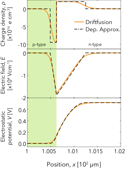
To convert the value obtained for into a uniform carrier generation rate, the short circuit flux density () was divided by the depletion region thickness , yielding . The complete parameter sets for the simulations in this section are given in Tables LABEL:tbl:Par_dep_approx_layers and LABEL:tbl:Par_dep_approx_device_wide.
Results
Both the analytical and numerical solutions for the space charge density, electric field, and electric potential are shown in Figure 11: The space charge widths, field strength and potential profiles all show good agreement.
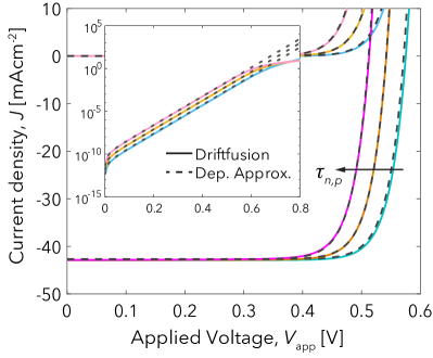
Figure 12 shows the light and dark current-voltage curves for the analytical solution obtained using equation 80, as compared to the numerical solutions from Driftfusion for three values of . For and the agreement is very good, even at current densities as low as A cm-2. The solutions begin to diverge at s, for which m such that and the underlying assumptions of the DA are no longer valid. The deviation from the ideal model in Driftfusion at higher current densities (Figure 12, inset) is expected due to the absence of series resistance in the DA.
5.2 Transient photovoltage response of a single layer field-free device
Analytical methods
To verify the time-dependence of the solution from Driftfusion, the transient photovoltage (TPV) response for a field-free slab of intrinsic semiconductor was calculated numerically and compared to results from a zero-dimensional (0-D) kinetic model. During a TPV experiment the device is illuminated at open circuit with a constant bias light and pulsed with an optical excitation source such as to produce a small additional photovoltage . As detailed in Supplemental Information Section LABEL:sec:TPV_derivation, it can be shown using a kinetic model that is given by:
| (85) |
| (86) |
where is the length of the laser pulse, is the additional volumetric generation rate due to the excitation pulse, is the steady-state open circuit carrier density, and is the decay rate constant of the TPV signal.
Simulation methods
A nm field-free single layer of semiconductor with eV was simulated in Driftfusion with the zero flux density boundary conditions for electronic carriers representing perfect blocking contacts. The constant volumetric generation rate was set to cm-3 s-1 sun equivalent based on the integrated photon flux density for the AMG solar spectrum and a step function absorption. In this special case the splitting of the quasi-Fermi levels in the simulation is solely attributable to changes in chemical potential, such that no series resistance term is needed for the potential boundary conditions. It should be noted that for instances where an electric field is present in the device these boundary conditions will not represent an open circuit condition; a high value for or a mirrored cell approach (see Ref. Calado2016 for details) should be used instead. The second order band-to-band recombination coefficient was set to cm3s-1 and SRH recombination was switched off. Since the underlying kinetic theory demands that the TPV perturbation must be small such that the additional carrier density , we used s and set the pulse intensity equivalent to be of the bias light intensity. The complete parameter sets for the simulations are given in Tables LABEL:tbl:Par_tpv_layers and LABEL:tbl:Par_tpv_device_wide.
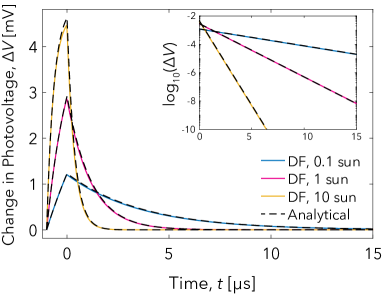
Results
A comparison of the results from the analytical and simulation models for bias light intensities of , , and sun equivalent is shown in Figure 13. The steady-state charge carrier densities and open circuit voltage obtained using Driftfusion agreed to within decimal places with the analytical values calculated using Equations LABEL:eq:n_btb and LABEL:eq:Voc_zero_D ( cm-3, V at 1 sun equivalent). The transient photovoltage perturbations also behaved as predicted, with the rate constants extracted from fitting the TPV decays correct to within significant figures of the values calculated using the analytical expression in Equation 86.
5.3 Numerical solution for three-layer devices with electronic carriers
Simulation methods
To verify that the graded treatment of the interfaces in Driftfusion produces similar results to models that use abrupt interfaces, a HTL/absorber/ETL device was simulated using both Driftfusion and the Advanced Semiconductor Analysis (ASA) simulation tool.Zeman2011 To maintain consistent layer dimensions the linear grid spacing for the ASA simulations and the interface thickness in Driftfusion were set to be nm.
The base material parameters for the active layer were based loosely on those for a perovskite material excluding mobile ionic charge. The parameters for the contact layers were not chosen to simulate real materials but rather to produce a large built-in potential and to vary as many properties as possible including the layer thickness, dielectric constants, recombination coefficients, mobilities etc. For optical generation the Beer-Lambert option (without back contact reflection) was chosen and the same optical constant and incident photon flux density spectrum data were used in both simulators. Four different parameter sets (PS) were compared, the key differences for which are summarised in the first four columns of Table 3.
| Parameter set | Description | Built-in voltage (V) | Active layer thickness (nm) | CB and VB effective density of states (cm-3) | ||
|---|---|---|---|---|---|---|
| HTL | Absorber | ETL | ||||
| 1a | 3-layer device based on MAPI active layer | 1.05 | 400 | |||
| 1b | As 1a with thinner active layer | 1.05 | 200 | |||
| 2a | Randomised layer properties | 0.6 | 200 | |||
| 2b | As 2a with uniform eDOS all layers | 0.6 | 200 | |||
The complete parameter sets for the simulated devices are given in Tables LABEL:tbl:Par_ASA1_layer - LABEL:tbl:Par_ASA2_device_wide.
Results: Beer-Lambert optical model
The results for the integrated generation rate profiles are shown in Figure LABEL:fig:DF_vs_ASA_gen. Despite the wavelength-dependent generation rates appearing to be very closely matched between the two simulators (Figure LABEL:fig:DF_vs_ASA_beer_lambert), the integration across photon energies resulted in marginally different generation profiles in the two simulations corresponding to a total difference in generation current of mA cm-2. As a means to ensure that the input generation profiles were identical, the generation profile from ASA was inserted into the Driftfusion parameters objects using the method described in Section 4.2.7.
Results: Current-voltage characteristics
To compare the current outputs from the different simulation tools current-voltage scans were performed from to V. Since ASA solves for the steady-state current, the - scan rate was set to be low ( V s-1) in Driftfusion to minimise contributions from the displacement current.
Figure 14a shows a comparison of the - characteristics obtained from the two simulation tools for Parameter Sets (PS) 1a and 2a. While the different parameter sets result in distinctly different characteristics for the two devices, the data show excellent agreement between the two simulators despite the significant difference in discretisation schemes and interface treatment.
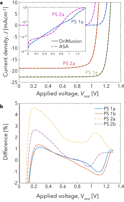
Closer examination of the results from the two simulators (Figure 14b) reveals that, the percentage difference (calculated as ) for PS 1a is on the order of % for current densities beyond A cm-2. Halving the active layer thickness has little impact on this difference (PS 1b). The percentage difference calculated for PS 2a, however, is much greater, with a maximum of % for current densities A cm-2. The larger difference between the two simulators in this instance can be attributed to a change of over orders of magnitude in the electron density at the absorber-ETL interface (Figure LABEL:fig:npx_DF_vs_ASA_ps2_0V) due to both a transition in the conduction band eDOS from to cm-3 and a change in the conduction band energy of eV. Under these circumstances the difference in discretisation schemes between the two tools becomes apparent: the linear discretisation method used in the PDEPE and Driftfusion cannot calculate the change in carrier densities within the interfaces to as high a degree of accuracy as the internal boundary conditions used in ASA (see Section LABEL:ssec:linear_discretisation for further details). The deviation can be reduced significantly, however, by using a uniform eDOS of cm-3 across all layers as the results for PS 2b show. With respect to device characteristics, despite the percentage difference in results for PS 2a, the key metrics of the - curve such as the , ideality factor and fill-factor are all preserved. Figure 15 shows a comparison of the electrostatic potential and hole density profiles calculated using Driftfusion and ASA for PS 1a under illumination at increasing applied bias. The electron density is given in the Supplemental Information, Figure LABEL:fig:DF_vs_ASA_nx_m1_1S. The agreement here between the solutions is excellent taking into consideration the difference in treatment of the interfaces between the two simulators.
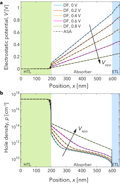
5.4 Numerical solution for three-layer devices with electronic and mobile ionic carriers
Courtier et al. recently published IonMonger,Courtier2019a a three-layer (HTL/absorber/ETL) drift-diffusion simulation tool for modelling perovskite solar cells which solves for coupled electron, hole and cation carrier distributions. In contrast to Driftfusion, IonMonger uses abrupt interfaces and solves carriers and the electrostatic potential for each of the three device layers simultaneously. The advantage to this approach is that boundary conditions can be established between the absorber and transport layers, such that interfacial recombination between electrons from one material and holes from another can be evaluated at the same grid point. The disadvantage is that variables are solved for simultaneously (minority carriers are not included in the transport regions) as opposed to in Driftfusion, for an equivalent three-layer device with a single mobile ionic species. Here we compare results obtained from Driftfusion with those from IonMonger for devices with similar parameter sets.
Methods
We modelled three layer perovskite HTL/absorber/ETL solar cells with electronic and mobile ionic carriers in the absorber layer and electronic carriers only in the HTL and ETL using IonMonger and Driftfusion. For the IonMonger simulations only holes were solved for within the HTL and electrons within the ETL. For the Driftfusion simulations all carriers were solved for in all regions with the ionic carrier mobility set to zero in the HTL, ETL and interfacial regions. Since the ionic carriers are inert and their charge is compensated by a static background charge density (see Equation 17) they have no effect in these regions. For the comparison we ran - scan simulations at a variety of scan speeds using similar parameter sets to those published in Ref. Courtier2019 : a device dominated by bulk recombination and a device dominated by interfacial recombination using the volumetric surface recombination scheme described in Section 3.7.3.
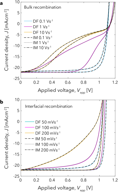
Results: Current-voltage characteristics
Figure 16a and 16b show the - results from Driftfusion (solid coloured curves) and IonMonger (black dashed curves) for the bulk and interfacial recombination dominated devices at varying voltage scan rates. The electrostatic potential profile, ionic carrier accumulation and electronic carrier profiles during the V s-1 forward scan for the bulk recombination device, and at mV s-1 for in the interfacial recombination dominated device, at increasing applied bias are given in the Supplemental Information Figures LABEL:fig:DF_vs_IM_solx and LABEL:fig:DF_vs_IM_solx_IR respectively. For both sets of parameters the results obtained from the two simulations are very similar with marginal differences in the calculated current outputs. This variance arises principally from the treatment of electronic currents across interfaces, differences in the spatial mesh, and calculation of ionic carrier densities throughout all layers of the device in Driftfusion as opposed to IonMonger, which introduces small additional integration errors into the space charge density (Supplemental Information Figure LABEL:fig:Ion_interfaces). For the device dominated by interfacial recombination (Figure 16b), additional errors are also introduced by the volumetric surface recombination scheme. Figure LABEL:fig:DF_vs_IM_rec_flux_compare shows that, while the scheme is self-consistent, differences arise from the surface carrier densities (specifically the electron density at the active layer-HTL interface). These differences are accentuated by increasing the energetic barriers to minority carriers from to eV (Equations 37 and 38) as shown in Supplemental Information Figure LABEL:fig:DF_vs_IM_interface_points. The differences can however be reduced by increasing the interface thickness and using a larger number of interface mesh points (Figure LABEL:fig:DF_vs_IM_interface_points). To this end, consistency with established analytical models that use abrupt interfaces is somewhat sacrificed in Driftfusion in favour of greater flexibility, which enables the physical models to be easily edited, devices with any number of material layers to be simulated and a range of interface-specific properties and grading functions to be specified.
We have verified Driftfusion against two analytical and two existing numerical models and found that in all cases the calculated results are in reasonably good agreement. The results show that the discrete interface approach produces results comparable to models with abrupt interfaces, albeit with marginal errors introduced owing to the combination of the interface treatment and the linear discretisation scheme used in Driftfusion.
6 Conclusions
We have developed an efficient and powerful one-dimensional drift-diffusion simulation tool for modelling semiconductor devices with mixed ionic-electronic conducting layers based on MATLAB’s pdepe toolbox. Distinct from existing codes, in addition to electronic carriers, Driftfusion can include up to two ionic carrier species and virtually any number of material layers. This flexibility is made possible by a discrete interlayer interface approach whereby the material properties can be graded between two adjoining semiconductor layers. This method has the added advantage that interface-specific properties can easily be specified.
The default physical models underlying the simulation were described and analytical approximations to the carrier densities and fluxes within the interfacial regions were given. Using these solutions, a method for approximating surface recombination within interfacial regions using a volumetric recombination scheme was derived.
The system architecture was presented and the processes by which users can define device properties and change the simulation’s physical model were outlined. Protocol functions, determining time-dependent voltage and light conditions, were described as well as the simulation solution structures and how to use built-in analysis and plotting functions to calculate and visualise outputs. A step-by-step guide was presented detailing how to create a device, find an equilibrium solution, and calculate current-voltage characteristics using a cyclic voltammogram protocol. Lastly, advanced features, including how to calculate multiple solutions in parallel, were briefly introduced.
Driftfusion was verified by comparing calculated solutions with two analytical and two existing numerical models which tested different aspects of the simulation. In all cases the agreement was good and the general device behaviour was reproduced. The discrete treatment of the interfaces resulted in small variations in the calculated currents as compared to other simulators using abrupt layer boundaries.
The ease with which the underlying models can be changed and new material layers can be introduced places Driftfusion in a unique space compared to other free-to-use simulation codes for which an intricate knowledge of the numerical mechanics is required to adapt the physical models and device architecture. By making Driftfusion both accessible and free-to-use our hope is that this work will advance our collective understanding of mixed ionic-electronic conducting materials and devices.
Acknowledgements.
The authors would like to thank the UK Engineering and Physical Sciences Research Council for funding this work (Grant No. EP/J002305/1, No. EP/M025020/1, No. EP/M014797/1, No. EP/N020863/1, No. EP/R020574/1, No. EP/R023581/ 1, and No. EP/L016702/1). J.N. thanks the European Research Council for support under the European Union’s Horizon 2020 research and innovation program (grant agreement No. 742708). We would also like to thank: Emilio Palomares and Davide Moia for lending the expertise of their students to work on this project, and Diego Alonso Álvarez for his invaluable advice on preparing and improving the code.Funding
The authors would like to thank the UK Engineering and Physical Sciences Research Council (grant No. EP/J002305/1, EP/M025020/1, EP/M014797/1, EP/R020574/1, EP/R023581/1, and EP/L016702/1) and the European Union’s Horizon 2020 research and innovation program grant agreement (grant No. 742708) for their support in funding this work.
Conflicts of interest
The authors declare that they have no conflicts of interest.
Availability of data and material
The data presented in this work is available at reasonable request from the authors.
Code availability
The simulation code is freely available at:
https://github.com/barnesgroupICL/Driftfusion
Authors’ contributions
P.C., P.R.F.B., I.G., M.A., and B.H. contributed to the development of the simulation code. P.C., P.R.F.B., J.N., I.G., and M.A. wrote the manuscript. P.R.F.B. and J.N. supervised the development and publication of this work.
References
- (1) W. Van Roosbroeck, Bell System Technical Journal 29(4), 560 (1950). DOI 10.1002/j.1538-7305.1950.tb03653.x
- (2) J.M. Foster, H.J. Snaith, T. Leijtens, G. Richardson, Siam J. Appl. Math 74(6), 1935 (2014). DOI 10.1137/130934258
- (3) S. van Reenen, M. Kemerink, H.J. Snaith, The Journal of Physical Chemistry Letters 6, 3808 (2015). DOI 10.1021/acs.jpclett.5b01645
- (4) G. Richardson, S.E. O’Kane, R.G. Niemann, T.A. Peltola, J.M. Foster, P.J. Cameron, A.B. Walker, Energy & Environmental Science 9, 1476 (2016). DOI 10.1039/C5EE02740C
- (5) M.T. Neukom, S. Züfle, E. Knapp, M. Makha, R. Hany, B. Ruhstaller, Solar Energy Materials and Solar Cells 169, 159 (2017). DOI 10.1016/j.solmat.2017.05.021
- (6) T.S. Sherkar, C. Momblona, L. Gil-Escrig, J. Ávila, M. Sessolo, H.J. Bolink, L.J.A. Koster, ACS Energy Letters 2(5), 1214 (2017). DOI 10.1021/acsenergylett.7b00236
- (7) M. García-Rosell, A. Bou, J.A. Jiménez-Tejada, J. Bisquert, P. Lopez-Varo, Journal of Physical Chemistry C 122(25), 13920 (2018). DOI 10.1021/acs.jpcc.8b01070
- (8) N.E. Courtier, J.M. Cave, J.M. Foster, A.B. Walker, G. Richardson, Energy & Environmental Science 12(1), 396 (2019). DOI 10.1039/C8EE01576G
- (9) L. Bertoluzzi, C.C. Boyd, N. Rolston, J. Xu, R. Prasanna, B.C. O’Regan, M.D. McGehee, Joule 4(1), 109 (2019). DOI 10.1016/j.joule.2019.10.003
- (10) Y. Huang, P. Lopez-Varo, B. Geffroy, H. Lee, J.E. Bourée, A. Mishra, P. Baranek, A. Rolland, L. Pedesseau, J.M. Jancu, J. Even, J.B. Puel, M. Gueunier-Farret, Journal of Photonics for Energy 10(02), 1 (2020). DOI 10.1117/1.jpe.10.024502
- (11) Z. Xiao, Y. Yuan, Y. Shao, Q. Wang, Q. Dong, C. Bi, P. Sharma, A. Gruverman, J. Huang, Nature Materials 14(February), 193 (2015). DOI 10.1038/nmat4150
- (12) C. Eames, J.M. Frost, P.R.F. Barnes, B.C. O’Regan, A. Walsh, M.S. Islam, Nature Communications 6, 7497 (2015). DOI 10.1038/ncomms8497
- (13) T.Y. Yang, G. Gregori, N. Pellet, M. Grätzel, J. Maier, Angewandte Chemie 127, 8016 (2015). DOI 10.1002/ange.201500014
- (14) J. Haruyama, K. Sodeyama, L. Han, Y. Tateyama, Journal of the American Chemical Society 137(32), 10048 (2015). DOI 10.1021/jacs.5b03615
- (15) D. Moia, I. Gelmetti, P. Calado, W. Fisher, M. Stringer, O. Game, Y. Hu, P. Docampo, D. Lidzey, E. Palomares, J. Nelson, P.R.F. Barnes, Energy Environ. Sci. 12(4), 1296 (2019). DOI 10.1039/C8EE02362J
- (16) P. Calado, D. Burkitt, J. Yao, J. Troughton, T.M. Watson, M.J. Carnie, A.M. Telford, B.C. O’Regan, J. Nelson, P.R. Barnes, Physical Review Applied 11(4), 044005 (2019). DOI 10.1103/PhysRevApplied.11.044005
- (17) S.E.J. O’Kane, G. Richardson, A. Pockett, R.G. Niemann, J.M. Cave, N. Sakai, G.E. Eperon, H.J. Snaith, J.M. Foster, P.J. Cameron, A.B. Walker, J. Mater. Chem. C 5(2), 452 (2017). DOI 10.1039/C6TC04964H
- (18) P. Calado, A.M. Telford, D. Bryant, X. Li, J. Nelson, B.C. O’Regan, P.R. Barnes, Nature Communications 7, 13831 (2016). DOI 10.1038/ncomms13831
- (19) FLUXiM AG. SETFOS: Semiconducting emissive thin film optics simulator (2019)
- (20) N.E. Courtier, J.M. Cave, A.B. Walker, G. Richardson, J.M. Foster, Journal of Computational Electronics 18(4), 1435 (2019). DOI 10.1007/s10825-019-01396-2
- (21) COMSOL AB. COMSOL Multiphysics (2019)
- (22) The Mathworks. MATLAB (2017)
- (23) D.A. Jacobs, H. Shen, F. Pfeffer, J. Peng, T.P. White, F.J. Beck, K.R. Catchpole, The Journal of Applied Physics 124, 225702 (2018). DOI 10.1063/1.5063259
- (24) N. Tessler, Y. Vaynzof, ACS Energy Letters 5, 1260 (2020). DOI 10.1021/acsenergylett.0c00172
- (25) A. Singh, W. Kaiser, A. Gagliardi, Solar Energy Materials and Solar Cells 221(October 2020), 110912 (2021). DOI 10.1016/j.solmat.2020.110912
- (26) P. Calado, P.R.F. Barnes, I. Gelmetti, M. Azzouzi, B. Hilton. Driftfusion (2017). DOI 10.5281/zenodo.3670155. URL https://github.com/barnesgroupICL/Driftfusion
- (27) S.M. Sze, Physics of semiconductor devices, 2nd edn. (John Wiley & Sons, Inc., New York, 1981)
- (28) J. Nelson, The physics of solar cells (Imperial College Press, 2003)
- (29) P. Calado, Transient optoelectronic characterisation and simulation of perovskite solar cells. Ph.D. thesis, Imperial College London (2017). URL https://spiral.imperial.ac.uk/handle/10044/1/66894
- (30) P.R.F. Barnes, A.Y. Anderson, J.R. Durrant, B.C. O’Regan, Phys. Chem. Chem. Phys. 13, 5798 (2011). DOI 10.1039/c0cp01554g
- (31) L.F. Shampine, J. Kierzenka. PDEPE (2013)
- (32) R.D. Skeel, M. Berzins, SIAM Journal on Scientific and Statistical Computing 11(1), 1 (1990). DOI 10.1137/0911001
- (33) A. Walsh, D.O. Scanlon, S. Chen, X.G. Gong, S.H. Wei, Angewandte Chemie International Edition 54, 1791 (2015). DOI 10.1002/anie.201409740
- (34) M.S. Kilic, M.Z. Bazant, A. Ajdari, Physical Review E - Statistical, Nonlinear, and Soft Matter Physics 75(2), 1 (2007). DOI 10.1103/PhysRevE.75.021502
- (35) M. Zeman, J. van den Heuvel, M. Kroom, J. Willemen, B. Pieters, J. Krc, S. Solntsev. Advanced Semiconductor Analysis (ASA) (2011). URL https://www.tudelft.nl/en/ewi/over-de-faculteit/afdelingen/electrical-sustainable-energy/photovoltaic-materials-and-devices/software-platform/asa-software
- (36) B.V. Zeghbroeck, Principles of semiconductor devices, online edn. (University of Colorado Boulder, Colorado Boulder, 2011)
- (37) W. Shockley, W.T. Read, Physical Review 87(46), 835 (1952). DOI 10.1103/PhysRev.87.835
- (38) W. Tress, Device physics of organic solar cells. Ph.D. thesis, Dresden University of Technology (2012)
- (39) N.E. Courtier, G. Richardson, J.M. Foster, Applied Mathematical Modelling 63, 329 (2018). DOI 10.1016/j.apm.2018.06.051
- (40) J.S. Blakemore, Solid State Electronics 25(11), 1067 (1982). DOI 10.1016/0038-1101(82)90143-5
- (41) P. Farrell, T. Koprucki, J. Fuhrmann, Journal of Computational Physics 346, 497 (2017). DOI 10.1016/j.jcp.2017.06.023
- (42) D. Alonso-Álvarez, T. Wilson, P. Pearce, M. Führer, D. Farrell, N. Ekins-Daukes, Journal of Computational Electronics 17, 1099 (2018). DOI 10.1007/s10825-018-1171-3
- (43) G.F. Burkhard, E.T. Hoke, M.D. McGehee, Advanced Materials 22(30), 3293 (2010). DOI 10.1002/adma.201000883
- (44) R.A. Belisle, W.H. Nguyen, A.R. Bowring, P. Calado, X. Li, S.J.C. Irvine, M.D. Mcgehee, P.R.F. Barnes, B.C. O’Regan, Energy & Environmental Science 10(1), 192 (2016). DOI 10.1039/C6EE02914K
- (45) W. Shockley, Bell Labs Technical Journal 28(3), 435 (1949). DOI 10.1002/j.1538-7305.1949.tb03645.x
- (46) G.F. Burkhard, E.T. Hoke, M.D. McGehee. Transfer Matrix Optical Modeling (2011). URL https://web.stanford.edu/group/mcgehee/transfermatrix/