vario\fancyrefseclabelprefixSection #1 \frefformatvariothmTheorem #1 \frefformatvariolemLemma #1 \frefformatvariocorCorollary #1 \frefformatvariodefDefinition #1 \frefformatvarioobsObservation #1 \frefformatvarioasmAssumption #1 \frefformatvario\fancyreffiglabelprefixFigure #1 \frefformatvarioappAppendix #1 \frefformatvariopropProposition #1 \frefformatvarioalgAlgorithm #1 \frefformatvario\fancyrefeqlabelprefix(#1) \frefformatvariotblTable #1
High-Bandwidth Spatial Equalization for mmWave Massive MU-MIMO with Processing-In-Memory
Abstract
All-digital basestation (BS) architectures enable superior spectral efficiency compared to hybrid solutions in massive multi-user MIMO systems. However, supporting large bandwidths with all-digital architectures at mmWave frequencies is challenging as traditional baseband processing would result in excessively high power consumption and large silicon area. The recently-proposed concept of finite-alphabet equalization is able to address both of these issues by using equalization matrices that contain low-resolution entries to lower the power and complexity of high-throughput matrix-vector products in hardware. In this paper, we explore two different finite-alphabet equalization hardware implementations that tightly integrate the memory and processing elements: (i) a parallel array of multiply-accumulate (MAC) units and (ii) a bit-serial processing-in-memory (PIM) architecture. Our all-digital VLSI implementation results in 28nm CMOS show that the bit-serial PIM architecture reduces the area and power consumption up to a factor of and , respectively, when compared to a parallel MAC array that operates at the same throughput.
Index Terms:
Millimeter wave (mmWave), massive multi-user MIMO, spatial equalization, quantization, digital ASIC design, processing-in-memory (PIM).I Introduction
Future wireless systems are expected to rely on millimeter wave (mmWave) communication [1] that provides extreme bandwidths, and massive multi-user multiple-input multiple-output (MU-MIMO) [2] that compensates for the path loss at mmWave frequencies and enables communication with multiple user equipments (UEs) in the same time-frequency resource. However, the combination of high-bandwidth mmWave communication with hundreds of basestation (BS) antenna elements inevitably results in excessively high baseband complexity and power consumption. In order to develop power-efficient BS designs for such systems, significant attention has been given to hybrid analog-digital architectures [3, 4, 5, 6, 7]. However, such hybrid solutions are limited in the number of transmission paths they can resolve simultaneously [7, 8, 9], thus degrading spectral efficiency. All-digital BS architectures are a promising alternative to mitigate this drawback [10, 11, 12]. While it is widely believed that all-digital BS architectures consume more power than hybrid solutions, recent results in [9, 11] indicate that the power consumption of radio-frequency (RF) and data converters in all-digital architectures is comparable to that of hybrid systems when reducing the data-converter resolution. Despite these recent findings, the power consumption and system costs of baseband processing for all-digital mmWave massive MU-MIMO architectures are largely unexplored.
I-A All-Digital Spatial Equalization
In the uplink, UEs transmit information to a BS equipped with antennas. To recover the transmitted signals, the BS must perform spatial equalization for each received sample. For linear equalization methods, one has to compute complex-valued matrix-vector products at the rate of the baseband analog-to-digital converters (ADCs). In mmWave massive MU-MIMO systems, even such straightforward matrix-vector products will result in power-hungry digital circuitry as we are dealing with extremely high sampling rates and large equalization matrices. For example, a conventional digital circuit that computes matrix-vector products for antennas and UEs at a rate of G vectors/s consumes W and occupies in nm CMOS [13]. The power and area will further increase when considering systems with more BS antennas, more UEs, and higher sampling rates. Consequently, all-digital BS architectures require efficient spatial equalization circuitry that minimizes power and area without degrading spectral efficiency.
The hardware complexity (in terms of power and area) of matrix-vector products can be reduced by decreasing the number of bits used to represent its operands. Previous work has focused extensively on reducing the received vector’s precision, which corresponds to the use of low-resolution ADCs (e.g., to bits) at the BS of massive MU-MIMO systems [7, 9, 10, 11, 14, 15]. The spatial equalization matrices, however, are typically represented using high-precision numbers (e.g., to bits) [16, 17]. Recently, reference [13] proposed finite-alphabet equalization, which represents equalization matrices with low-resolution numbers while minimizing the post-equalization mean-square error (MSE). In [13], finite-alphabet equalization was shown to reduce the equalization power and area by and , respectively, when using conventional digital very-large scale integration (VLSI) designs.
I-B Processing-In-Memory (PIM)
While the performance of digital VLSI designs continuously increased over many decades, memory access times have not improved at the same pace. This disparity led to a so-called “memory-wall” [18] in which communication with memories causes a major bottleneck in terms of throughput and energy efficiency. Processing-in-memory (PIM) is an emerging compute paradigm that aims at avoiding the memory wall by co-locating logic close to memories, with the goal of minimizing time and energy required for data movement [19]. With the looming end of Moore’s Law, PIM has caught increasing attention. Existing PIM approaches focus on incorporating logic into memory processes [20], exploiting mixed-signal techniques [21], using emerging devices [22], or relying on standard CMOS logic processes with all-digital processing [23].
I-C Contributions
Traditional application-specific integrated circuit (ASIC) designs are closely related to PIM, as design-specific memory structures are placed near computation elements in order to maximize throughput and energy efficiency. However, with the recent appearance of numerous PIM architectures, it is natural to ask whether PIM is useful for next-generation wireless systems, a domain which has largely benefitted from ASIC designs in the past. To shed light on this question, we evaluate two distinct VLSI designs that implement finite-alphabet equalization. The first design corresponds to an array of all-digital multiply-accumulate (MAC) units, which represents traditional ASICs. The second design corresponds to a PIM approach, which equips the bit-cells of a memory array with XNOR functionality to enable efficient, massively-parallel low-resolution matrix-vector products. To enable a fair comparison between PIM and traditional ASIC designs, we use a specialized version of the recently-proposed, all-digital PPAC, which stands for Parallel Processor in Associative Content addressable memory (CAM) [23]. For the same finite-alphabet equalization throughput, we compare both solutions in terms of area and power consumption for a nm CMOS technology.
I-D Notation
Uppercase bold letters denote matrices; lowercase, column vectors. For a matrix , the transpose, Hermitian transpose, real and imaginary parts are , , , and , respectively. For a vector , the th entry is , the -norm is , and the entry-wise complex conjugate is . is the expectation operator with respect to the random vector .
II Spatial Equalization
II-A System Model and Spatial Equalization Basics
We consider the uplink of a narrowband111Our analysis is also suitable for wideband channels in combination with orthogonal frequency-division multiplexing (OFDM), where the input-output relation of each subcarrier can also be modeled as in \frefeq:channelmodel. mmWave massive MU-MIMO system where a -antenna BS receives signals from single-antenna UEs. The uplink narrowband input-output relation is modeled as
| (1) |
where is the received vector at the BS, is the known uplink MIMO channel matrix, is the transmit data vector, with being the constellation set (e.g., 16-QAM), and is i.i.d. circularly-symmetric complex Gaussian noise with variance per entry. We assume that the covariance matrix of is . Furthermore, we assume perfect channel state information at the BS.
Spatial equalization produces an estimate of the transmit data vector given and . With linear equalization, the estimate can be computed as
| (2) |
with the spatial equalization matrix . Typically, is chosen to minimize the MSE defined as
| (3) |
which results in the linear minimum MSE (L-MMSE) equalizer, given by [24]
| (4) |
with . The complex-valued entries of the L-MMSE equalizer are routinely represented with high-resolution numbers (e.g., to bits [16, 17]). For high-bandwidth mmWave massive MU-MIMO systems, such resolution leads to excessively large and power-hungry VLSI circuits.
II-B Finite-Alphabet Equalization
To arrive at more efficient equalization circuitry, finite-alphabet equalization, put forward in [13], proposes to use finite-alphabet equalization matrices with the following structure:
| (5) |
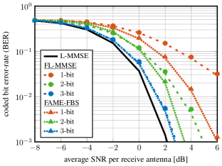
Here, is a low-resolution matrix whose entries come from a low-cardinality finite alphabet (e.g., the “1-bit” alphabet is ), and contains per-UE high-resolution scaling factors. The work in [13] proposes two ways to compute a finite-alphabet matrix with the form in \frefeq:FAMEmatrix: (i) quantizing the L-MMSE matrix in \frefeq:lmmse to a finite-alphabet, called FL-MMSE, and (ii) approximately solving the finite-alphabet MMSE equalization (FAME) problem using forward-backward splitting, called FAME-FBS. \freffig:ber, which is adopted from [25, Fig. 2(b)], clearly demonstrates that FAME-FBS enables superior error-rate performance, even when considering transmission over realistic, QuaDRiGa-generated [26] mmWave non-line-of-sight channels. We note that FAME-FBS outperforms FL-MMSE as it computes finite-alphabet equalization matrices that minimize the MSE in \frefeq:mse.
Regardless of how the finite-alphabet matrices are computed, the structure in \frefeq:FAMEmatrix enables efficient hardware implementations as per-UE equalization becomes
| (6) |
where and are the th rows of and , respectively. Since has low-precision entries, the inner product (requiring complex-valued scalar multiplications) can be computed efficiently using low-precision circuitry (e.g., adders and subtractors for the 1-bit case). The low-resolution inner product is then scaled by , a scalar operation that is carried out at higher resolution, but only once per UE.
III VLSI Architectures
We will now detail three different VLSI architectures that implement finite-alphabet equalization. All of these architectures tightly integrate the datapath and memory to achieve high throughput and energy efficiency. The first and second architectures achieve such integration with a traditional ASIC design approach—the third one relies on all-digital PIM.
We consider VLSI architectures that perform matrix-vector multiplications with a finite-alphabet equalization matrix . Furthermore, we assume that the low-resolution part of such matrix is represented with a symmetric set of mid-rise quantized numbers, e.g., the -bit alphabet has entries whose real and imaginary parts are in the set . We represent the entries of using two’s complement numbers.
III-A Linear Array of MAC Units
As a baseline, we consider the architecture in [13], which corresponds to a linear array of complex-valued MAC units (one per UE). Each MAC unit reads data from a memory storing the corresponding -dimensional row of and all MAC units receive one entry of per clock cycle. Thus, the inner product is computed in clock cycles. The result is then scaled by using a high-resolution multiplier.
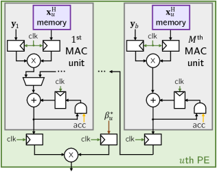
III-B Optimized MAC Array
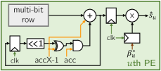
The hardware efficiency of the baseline array of MAC units in [13] can be optimized by means of replication. As shown in \freffig:mvp, we propose to use, for each UE, one processing element (PE) that consists of MAC units, each MAC unit having access to a -dimensional partition of . Then, each MAC unit within a PE receives different entries of to compute the inner-product between its partitions of and in clock cycles. The results are then merged together to complete the inner product . This final reduction is achieved by reusing the adders in the MAC units following a binary-tree structure, which takes clock cycles.
III-C PPAC: Parallel Processor in Associative CAM
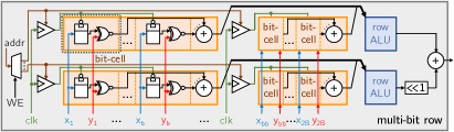
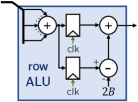
The PPAC architecture proposed in [23] is an all-digital CMOS PIM implementation in which every bit-cell of a memory is capable of multiplying its stored -bit value with an external -bit input using a bipolar (XNOR) or unipolar (AND) product. All products in a row are summed together by a population count in an arithmetic logic unit (ALU) associated with each row. Each row ALU can further process the population count to accelerate a range of operations, including the execution of a -bit matrix-vector product in a single clock cycle. In this work, we simplify the PPAC architecture to the one illustrated in \freffig:ppac, so that it only supports the matrix-vector products of interest for spatial equalization; see [23] for more details on PPAC.
| resolution [bit] | |||
|---|---|---|---|
| Silicon area [] | 0.164 | 0.324 | 0.483 |
| Clock frequency [MHz] | 796 | 785 | 784 |
| Throughput [M vectors/s] | 113.7 | 112.1 | 112.0 |
| Power consumption222Extracted from stimuli-based post-layout simulations in the typical-typical process corner at with a nominal power supply of 0.9V. [mW] | 112 | 246 | 383 |
| resolution [bits] | 4 | 7 | ||||||||||||||||
| Equalizer | Original MAC | Optimized MAC | PPAC | Original MAC | Optimized MAC | PPAC | ||||||||||||
| resolution [bit] | ||||||||||||||||||
| Silicon area [] | 21 | 32 | 42 | 4.1 | 7.0 | 8.6 | 1.8 | 3.6 | 5.3 | 22 | 33 | 43 | 5.6 | 9.8 | 11 | 3.0 | 5.8 | 8.7 |
| Power consumption333Extracted from stimuli-based post-layout simulations in the typical-typical process corner at with a nominal power supply of 0.9V. [W] | 5.0 | 8.3 | 11.8 | 3.8 | 7.2 | 9.1 | 1.2 | 2.7 | 4.2 | 7.2 | 12.0 | 15.9 | 6.4 | 11.1 | 14.2 | 2.0 | 4.4 | 6.9 |
As in [23], our customized PPAC implementation supports multi-bit vectors in a bit-serial manner: For an input vector with -bit entries, we first input a vector which contains the most significant bit of all entries, and we compute , where is stored in the PPAC memory. This process is repeated times, while accumulating the new result to the previous result (cf. \freffig:ppac_pe) to compute . In contrast to [23], we implement multi-bit matrix operations by having a different row for each bit-significance of a matrix entry: If the matrix has -bit entries, we use PPAC rows to represent one matrix row. The results coming from each row are combined using arithmetic shifts and additions (cf. \freffig:ppac_row). Hence, each partial product , , is computed in a single clock cycle, completing in clock cycles.
While PPAC naturally operates on real-valued numbers, spatial equalization requires complex-valued operations. We use the real-valued decomposition of both and , i.e., we store in PPAC and apply at the inputs, where
As a result, the complex-valued matrix-vector product between a matrix with -bit entries and a vector with -bit entries is computed in clock cycles using a PPAC array that has rows, each one with bits. The resulting -dimensional vector is scaled with using one complex-valued multiplier per UE (cf. \freffig:ppac_pe), for a total of multipliers. The markers in \freffig:ber correspond to the fixed-point performance of our hardware design, which exhibits virtually no implementation loss when compared to double-precision floating-point arithmetic (represented by the curves).
IV VLSI Design Comparison
IV-A Comparison Methodology
We now compare VLSI implementation results for the different architectures described in \frefsec:arch. We follow the procedure in [13], where, for each equalizer resolution , a single instance of each VLSI architecture is placed-and-routed in nm CMOS. Power is measured only for matrix-vector products, not for initializing the memories. \freftbl:implresultsoneppac provides implementation results for PPAC. Since the throughput offered by a single PPAC instance is not sufficient to reach the throughputs targeted by future mmWave systems, we use several parallel instances in a time-interleaved manner to reach a target throughput of G vectors/s. For example, for the case described in \freftbl:implresultsoneppac, we need PPAC instances when operating with a 1-bit equalizer. Then, we scale the area and power numbers proportionally to the number of instances.
The results for the linear array of MAC units are taken directly from [13], while the ones for PPAC are obtained from our own VLSI designs. The results for the optimized MAC array are estimated from the linear array of MAC units in the following way: For a design with -bit equalizer resolution, let be the fraction of silicon area occupied by the MAC units, excluding the -memories, in the implementation results of the linear array of MAC units from [13]. Then, corresponds to the fraction of the area occupied by the rest of the design, including the -memories and -scaling multipliers. As a result, the area occupied by the optimized MAC array with MAC units per PE can be modeled as times the area of the original array. We follow the same procedure to estimate the power consumption of the optimized MAC array. To compute the throughput of the optimized MAC array, we take the clock frequency of the original array from [13], and model the latency of the optimized array with clock cycles, as described in \frefsec:repmac. We choose the parameter that minimizes the -product while being a power of two to perform reduction as described for the optimized MAC array.
IV-B Comparison of Finite-Alphabet Equalizers
tbl:implresults shows implementation results for a system with antennas, UEs, and for a target throughput of G vectors/s for the cases where the equalizer resolution is bits and the received vector resolution is bits. For the optimized MAC array, we use MAC units per UE. We observe that the optimized MAC array improves the circuit area of the original array by more than ; this is because the MAC units occupy no more than of the original design’s area, so that replication does not increase the per-instance area significantly, but has a significant impact on the per-instance throughput, requiring fewer instances to meet the target throughput. While there are fewer instances, each instance contains more MAC units, which draw up to of the initial design’s power. As a result, both MAC arrays consume roughly the same amount of power.
By comparing the optimized MAC array results to those of PPAC, we observe that PPAC achieves a significant reduction in silicon area and power consumption for all the considered cases. For example, when considering -bit finite-alphabet equalizers with -bit inputs, we see that PPAC reduces the area and power consumption by a factor of and , respectively. However, these area and power consumption savings decrease as the equalizer resolution increases: When using a -bit equalizer with -bit inputs, PPAC offers and lower area and power consumption, respectively. These results illustrate that bit-serial PIM architectures provide benefits not only in scenarios that need a massive amount of memory, but also in applications that require hardware implementations with low area and power, where ASICs have been used traditionally. We finally emphasize that the theoretical advantages of PIM can already be realized with an all-digital architecture implemented in standard CMOS technology, as demonstrated by our PPAC results.
V Conclusions
We have implemented finite-alphabet equalization for mmWave massive MU-MIMO systems using traditional ASIC architectures and a PIM architecture. Our implementation results have shown that an all-digital PIM solution reduces the silicon area and power consumption by at least a factor of and , respectively, compared to a conventional ASIC. Combined with the savings provided by finite-alphabet equalization (up to and reduction in area and power consumption, respectively), PIM architectures pave the way for high-throughput and low-power all-digital BS architectures.
There are many avenues for future work. A system-level analysis that studies the effects of the different input interfaces used by the considered architectures is in order. Furthermore, other PIM designs that use, e.g., mixed-signal techniques or that rely on emerging devices, should be considered, as they could achieve superior throughput, area, and power consumption.
References
- [1] A. L. Swindlehurst, E. Ayanoglu, P. Heydari, and F. Capolino, “Millimeter-wave massive MIMO: The next wireless revolution?” IEEE Commun. Mag., vol. 52, no. 9, pp. 56–62, Sep. 2014.
- [2] E. G. Larsson, F. Tufvesson, O. Edfors, and T. L. Marzetta, “Massive MIMO for next generation wireless systems,” IEEE Commun. Mag., vol. 52, no. 2, pp. 186–195, Feb. 2014.
- [3] W. Roh, J.-Y. Seol, J. Park, B. Lee, J. Lee, Y. Kim, J. Cho, K. Cheun, and F. Aryanfar, “Millimeter-wave beamforming as an enabling technology for 5G cellular communications: Theoretical feasibility and prototype results,” IEEE Commun. Mag., vol. 52, no. 2, pp. 106–113, Feb. 2014.
- [4] B. Sadhu, Y. Tousi, J. Hallin, S. Sahl, S. Reynolds, Ö. Renström, K. Sjögren, O. Haapalahti, N. Mazor, B. Bokinge, G. Weibull, H. Bengtsson, A. Carlinger, E. Westesson, J. Thillberg, L. Rexberg, M. Yeck, X. Gu, D. Friedman, and A. Valdes-Garcia, “A 28GHz 32-element phased-array transceiver IC with concurrent dual polarized beams and 1.4 degree beam-steering resolution for 5G communication,” in IEEE Int. Solid-State Circuits Conf. (ISSCC), Feb. 2017, pp. 128–129.
- [5] J. Du, W. Xu, H. Shen, X. Dong, and C. Zhao, “Hybrid precoding architecture for massive multiuser MIMO with dissipation: Sub-connected or fully connected structures?” IEEE Trans. Wireless Commun., vol. 17, no. 8, pp. 5465–5479, Aug. 2018.
- [6] R. Magueta, D. Castanheira, A. Silva, R. Dinis, and A. Gameiro, “Hybrid multi-user equalizer for massive MIMO millimeter-wave dynamic subconnected architecture,” IEEE Access, vol. 7, pp. 79 017–79 029, 2019.
- [7] A. Alkhateeb, J. Mo, N. González-Prelcic, and R. W. Heath Jr., “MIMO precoding and combining solutions for millimeter-wave systems,” IEEE Commun. Mag., vol. 52, no. 12, pp. 122–131, Dec. 2014.
- [8] E. Björnson, L. Van der Perre, S. Buzzi, and E. G. Larsson, “Massive MIMO in sub-6 GHz and mmWave: Physical, practical, and use-case differences,” IEEE Wireless Commun., vol. 26, no. 2, pp. 100–108, Apr. 2019.
- [9] S. Dutta, C. N. Barati, A. Dhananjay, D. A. Ramirez, J. F. Buckwalter, and S. Rangan, “A case for digital beamforming at mmWave,” IEEE Trans. Wireless Commun., vol. 19, no. 2, pp. 756–770, Feb. 2020.
- [10] J. Mo and R. W. Heath Jr., “Capacity analysis of one-bit quantized MIMO systems with transmitter channel state information,” IEEE Trans. Signal Process., vol. 63, no. 20, pp. 5498–5512, Oct. 2015.
- [11] K. Roth and J. A. Nossek, “Achievable rate and energy efficiency of hybrid and digital beamforming receivers with low resolution ADC,” IEEE J. Sel. Areas Commun., vol. 35, no. 9, pp. 2056–2068, Sep. 2017.
- [12] S. Jacobsson, G. Durisi, M. Coldrey, U. Gustavsson, and C. Studer, “Throughput analysis of massive MIMO uplink with low-resolution ADCs,” IEEE Trans. Wireless Commun., vol. 16, no. 6, pp. 4038–4051, Jun. 2017.
- [13] O. Castañeda, S. Jacobsson, G. Durisi, T. Goldstein, and C. Studer, “Finite-alphabet MMSE equalization for all-digital massive MU-MIMO mmWave communication,” IEEE J. Sel. Areas Commun., vol. 38, no.9, pp. 2128–2141, Sep. 2020.
- [14] C. Studer and G. Durisi, “Quantized massive MU-MIMO-OFDM uplink,” IEEE Trans. Commun., vol. 64, no. 6, pp. 2387–2399, Jun. 2016.
- [15] H. Yan, S. Ramesh, T. Gallagher, C. Ling, and D. Cabric, “Performance, power, and area design trade-offs in millimeter-wave transmitter beamforming architectures,” IEEE Circuits Syst. Mag., vol. 19, no. 2, pp. 33–58, May 2019.
- [16] C. Studer, S. Fateh, and D. Seethaler, “ASIC implementation of soft-input soft-output MIMO detection using MMSE parallel interference cancellation,” IEEE J. Solid-State Circuits, vol. 46, no. 7, pp. 1754–1765, Jul. 2011.
- [17] M. Wu, B. Yin, G. Wang, C. Dick, J. R. Cavallaro, and C. Studer, “Large-scale MIMO detection for 3GPP LTE: Algorithms and FPGA implementations,” IEEE J. Sel. Topics Signal Process., vol. 8, no. 5, pp. 916–929, Oct. 2014.
- [18] W. A. Wulf and S. A. McKee, “Hitting the memory wall: Implications of the obvious,” ACM SIGARCH Comput. Archit. News, vol. 23, no. 1, pp. 20–24, Mar. 1995.
- [19] R. Nair, “Evolution of memory architecture,” Proc. IEEE, vol. 103, no. 8, pp. 1331–1345, Aug. 2015.
- [20] S. Li, D. Niu, K. T. Malladi, H. Zheng, B. Brennan, and Y. Xie, “DRISA: A DRAM-based reconfigurable in-situ accelerator,” in IEEE/ACM Int. Symp. Microarchit. (MICRO), Oct. 2017, pp. 288–301.
- [21] H. Jia, Y. Tang, H. Valavi, J. Zhang, and N. Verma, “A microprocessor implemented in 65nm CMOS with configurable and bit-scalable accelerator for programmable in-memory computing,” arXiv preprint arXiv:1811.04047, Nov. 2018.
- [22] Q. Guo, X. Guo, R. Patel, E. Ipek, and E. G. Friedman, “AC-DIMM: Associative computing with STT-MRAM,” ACM SIGARCH Comput. Archit. News, vol. 41, no. 3, pp. 189–200, Jun. 2013.
- [23] O. Castañeda, M. Bobbett, A. Gallyas-Sanhueza, and C. Studer, “PPAC: A versatile in-memory accelerator for matrix-vector-product-like operations,” in IEEE Int. Conf. Appl.-specific Syst., Archit. and Processors (ASAP), Jul. 2019, pp. 149–156.
- [24] A. Paulraj, R. Nabar, and D. Gore, Introduction to space-time wireless communications. Cambridge Univ. Press, 2003.
- [25] O. Castañeda, S. Jacobsson, G. Durisi, T. Goldstein, and C. Studer, “Soft-output finite alphabet equalization for mmWave massive MIMO,” in Proc. IEEE Int. Conf. Acoust., Speech, Signal Process. (ICASSP), May 2020, pp. 1763–1767.
- [26] S. Jaeckel, L. Raschkowski, K. Börner, and L. Thiele, “QuaDRiGa: A 3-D multi-cell channel model with time evolution for enabling virtual field trials,” IEEE Trans. Antennas Propag., vol. 62, no. 6, pp. 3242–3256, Jun. 2014.