The ABC130 barrel module prototyping programme for the ATLAS strip tracker
Abstract
For the Phase-II Upgrade of the ATLAS Detector [1], its Inner Detector, consisting of silicon pixel, silicon strip and transition radiation sub-detectors, will be replaced with an all new 100 % silicon tracker, composed of a pixel tracker at inner radii and a strip tracker at outer radii. The future ATLAS strip tracker will include 11,000 silicon sensor modules in the central region (barrel) and 7,000 modules in the forward region (end-caps), which are foreseen to be constructed over a period of 3.5 years. The construction of each module consists of a series of assembly and quality control steps, which were engineered to be identical for all production sites. In order to develop the tooling and procedures for assembly and testing of these modules, two series of major prototyping programs were conducted: an early program using readout chips designed using a 250 nm fabrication process (ABCN-25) [2] [3] and a subsequent program using a follow-up chip set made using 130 nm processing (ABC130 and HCC130 chips). This second generation of readout chips was used for an extensive prototyping program that produced around 100 barrel-type modules and contributed significantly to the development of the final module layout. This paper gives an overview of the components used in ABC130 barrel modules, their assembly procedure and findings resulting from their tests.
1 Introduction
For the High-Luminosity Upgrade of the Large Hadron Collider, the ATLAS [1] Inner Detector will be replaced with a new, all silicon Inner Tracker (ITk), composed of a pixel tracker [4] and a strip tracker [5].
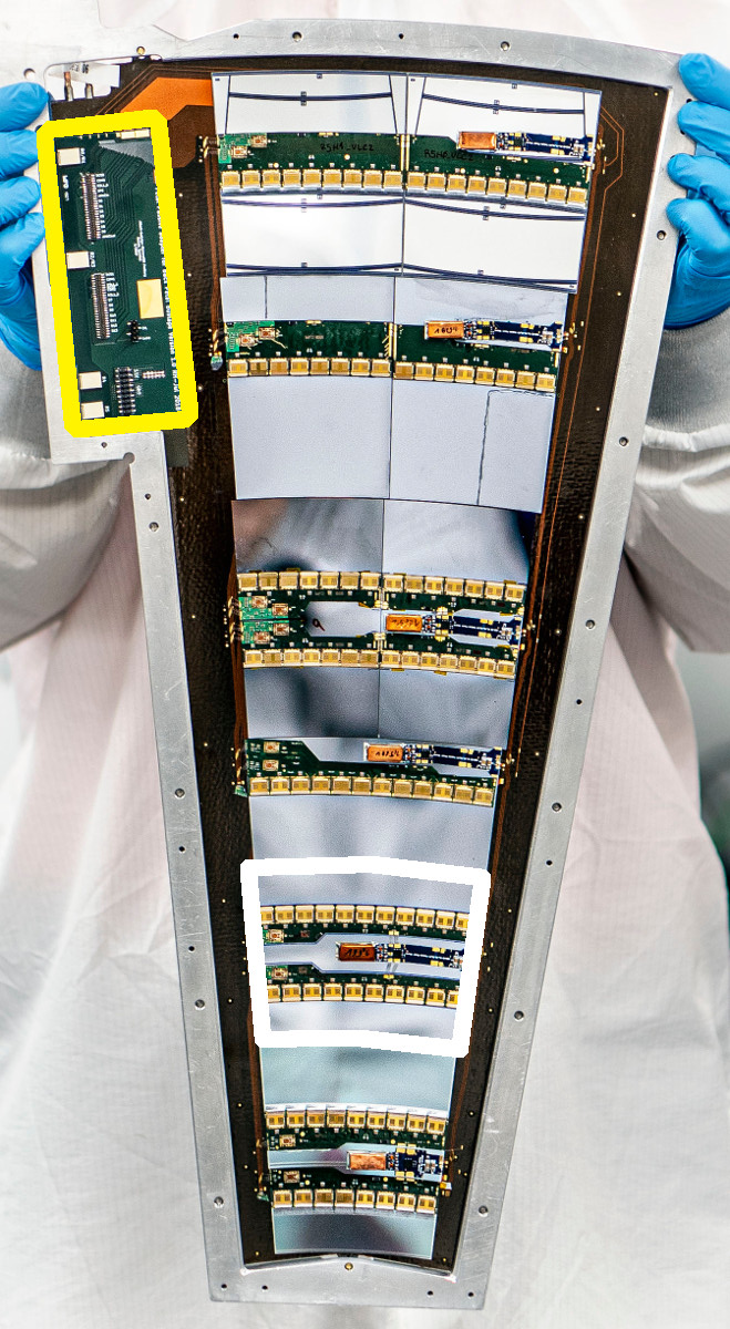
The main component of the ITk strip tracker is the module, comprising a silicon strip sensor, multiple custom readout chips mounted on a electronic circuit, called a hybrid, and a powerboard. In the central region of the ITk strip detector, the four barrel layers comprise 11,000 modules mounted on staves such that the sensors are arranged parallel to the beam axis (see figure 1(a)). The two end-caps in the forward region are constructed from six disks supporting a total of 7,000 modules mounted on petals such that the sensors are arranged orthogonal to the beam axis (see figure 1(b)).
Modules in the strip tracker barrel and end-caps were designed to contain the same materials and components, which have the same functionality, but different geometries. Only two types of sensors are used in the barrel region, whereas six sensor geometries are required for hermetic coverage of the end-cap. Here, only modules designed for the barrel region are presented.
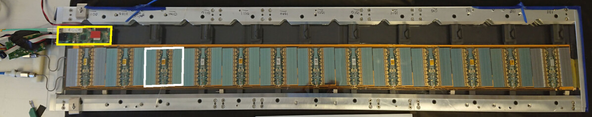
An extensive prototyping program was conducted in preparation for the production of 11,000 barrel modules at ten construction sites in the US, UK and China. The aim of the prototyping programme was to develop realistic tests of the concepts for tooling and assembly, readout software and testing procedures, hence, the prototype modules use readout chips, sensors and other components similar to those foreseen to be used in production.
2 Components
In the central region of the ITk strip tracker (barrel), two versions of modules are used:
-
•
short strip (SS) modules in the inner two barrel layers, where each sensor strip has a length of about 2.5 cm
-
•
long strip (LS) modules in the outer two barrel layers, with sensor strip lengths of about 5 cm
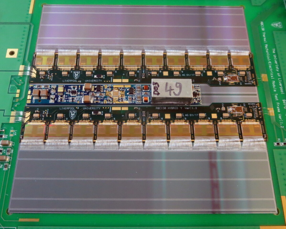
Despite their different strip lengths, both module types have similar sizes, which are determined by the size of the silicon strip sensor (about cm2 each). Therefore, strips are arranged in two rows on LS sensors and in four rows on SS sensors (the terms row and segment are used interchangeably throughout this manuscript), where each row consists of 1280 signal strips and two unconnected edge strips (see figures 2(a) and 2(b)). Accordingly, LS modules require 2560 readout channels (corresponding to 10 ABC130 readout chips with 256 channels each) and SS modules 5120 (corresponding to 20 ABC130 readout chips).
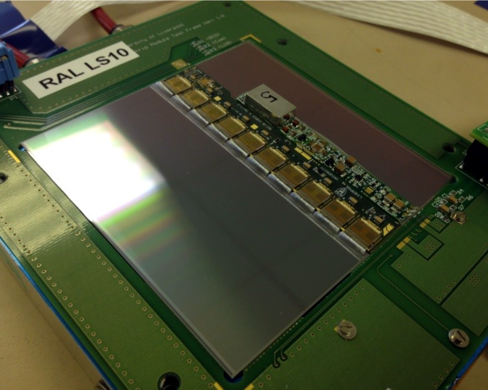
Despite requiring different numbers of readout channels and chips, electronic components for barrel modules were designed to be compatible with both sensor geometries. Flexible circuit boards supporting ABC130 readout chips, called hybrids (section 2.3), were designed, with one hybrid required per two strip segments. An SS module uses two such hybrids, an X-type and a Y-type version, whereas an LS module uses only one X-type hybrid (see figures 3(a) and 3(b)). Flex circuit boards called powerboards (section 2.4), which support a DCDC power converter, high voltage switch and a monitoring chip, match both LS and SS module layouts, thereby minimising the number of components to be designed, tested and qualified for production.
2.1 Sensors
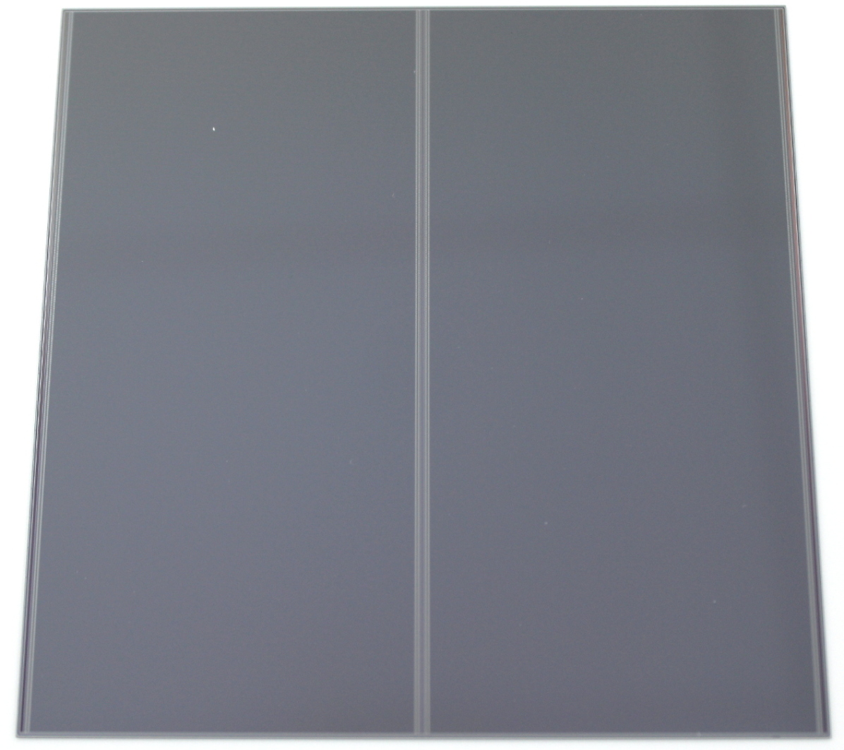
Short strip modules for the ABC130 barrel module program were constructed using ATLAS12 barrel sensors [6], a prototype version of the sensors to be used in the ATLAS ITk developed from the predecessor ATLAS07 sensors [7]. The sensors are fabricated from 6-inch floatzone wafers in a single-sided process.
The sensors have a nominal thickness of with a maximum thickness variation of 10 m across the sensor area. After dicing, ATLAS12 sensors have a size of . Compared to ATLAS07 sensors, the dead space in periphery of the sensor was reduced from approximately 1 mm to 500 m per edge.
Each ATLAS12SS sensor consists of four segments with 1282 strip implants each, where the first and last strip serve as field shaping strips. The strips have a length of and a strip pitch of 74.5 m.
In order to cope with the high-radiation environment of the ITk, strip sensors are made from p-doped bulk material with n+-doped strip implants. The bulk remains as p-doped after radiation damage, therefore the sensor depletion zone grows from the strip implant side towards the backside, allowing for a significant signal collection even when operated underdepleted due to radiation damage at the end-of life fluence. Each n+-doped strip implant is connected to an n-doped implant ring surrounding all strip implants (bias ring) to hold all strip implants at the same potential during operation. The bias ring is surrounded by another n-doped implant ring (guard ring) and a p-doped implant ring (edge ring) laid-out next to the dicing edge. Figure 4 shows an overview of the different sensor design features. This edge ring prevents the depleted region, evolving from the bias ring, from extending to and along the dicing edge between the edge ring and the p-doped backplane (held at high voltage), and is needed to prevent an early breakdown [8]. Detailed studies of the electrical properties of the ATLAS12 can be found in [9].
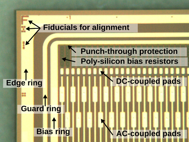
With increasing radiation damage, the Si/SiO2 passivation layer on the sensor surface will experience a build-up of defects and suffer from the surface damage of the ionising dose, which could lead to a short circuiting of the n+-strip implants. This is prevented using an inter-strip isolation technique based on p-stop traces, which was chosen out of several options tested on ATLAS07 devices. The sensor design also includes a protection structure for the AC coupling of the strips against beam splashes, a so called gated Punch Trough Protection [10]. The gated PTP design of the ATLAS12 sensors extends the strip below the bias resistor, leaving a 20 m gap to the bias rail and the gap covered by the extended sheet of the bias rail, which results in a hard breakdown across this gap in case of an excessive potential.
Another novelty of the ATLAS12 is the staggered design of the bond pads to match the four rows of bond pads on ABC130 ASICS (see section 2.2.1) to facilitate wire bonding. The bond pad design in the sensor mirrors the bond pad arrangement of the ABC13 ASICS, which results in a four row bonding process, where each subsequent row increases in height.
During the development of ATLAS12 sensors, it was discovered that they were sensitive to humidity [11]. This meant sensor breakdown, indicated by high leakage current, at reverse bias voltages below the nominal operating voltage of -500 V was observed at ambient humidity levels. Therefore, a protocol was established over the course of the ABC130 barrel module program, which required a minimisation of sensor exposure to higher humidity levels to prevent early breakdowns:
-
•
storage of sensors at modules at a maximum of 10 % humidity
-
•
sensor tests to be performed at maximum relative humidity of 20 %
-
•
minimisation of time sensors spent outside of dry storage, e.g. assembly
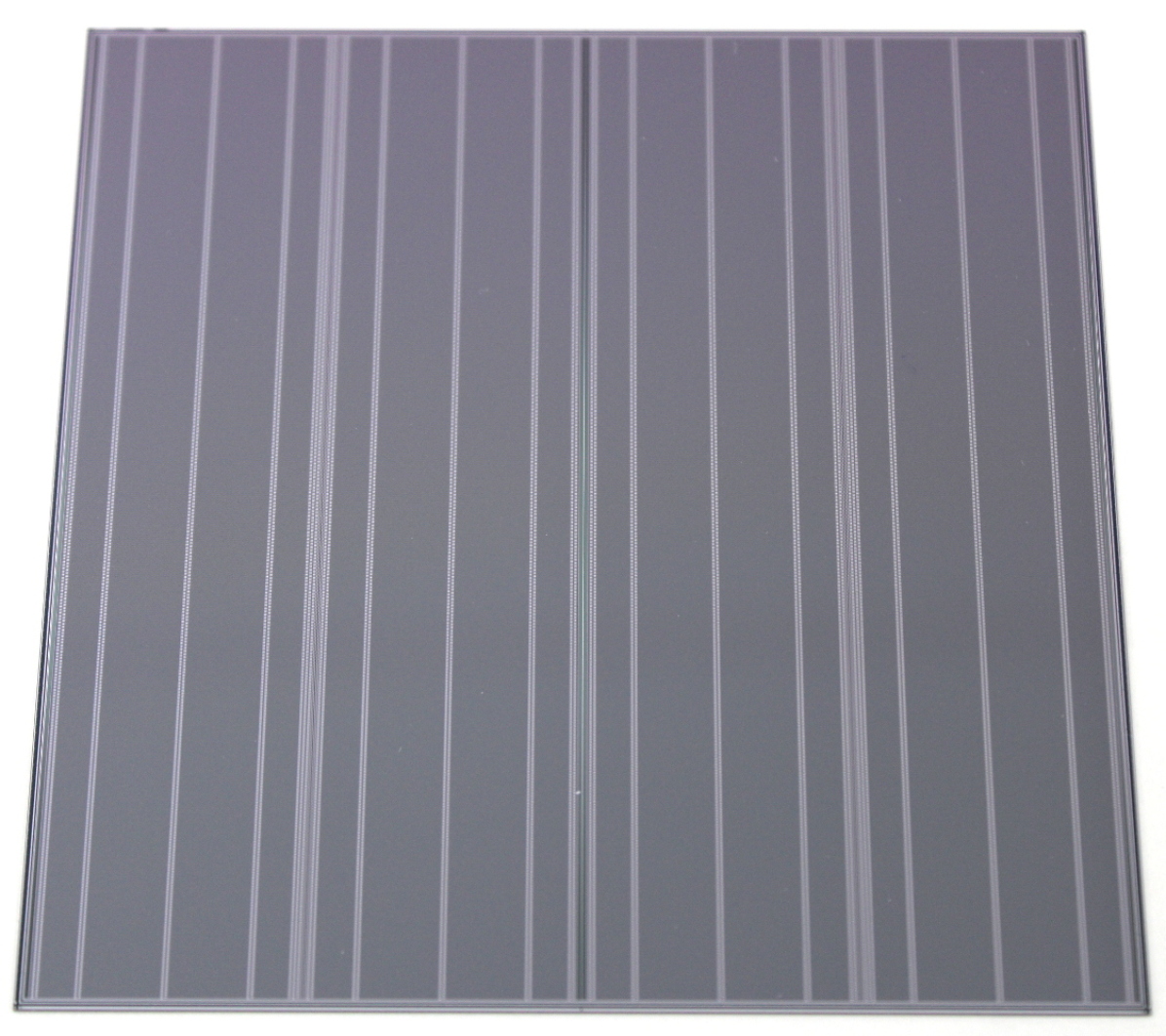
In addition to the construction of short strip modules, several long strip modules were constructed using ATLAS17LS sensors [12], which were developed after ATLAS12 sensors to prototype the long strip geometry. In contrast to the ATLAS12, the ATLAS17LS sensors are slightly larger with dimensions of , utilising the full usable area out of 6-inch wafer. ATLAS17LS sensors have a strip pitch of 75.5 m and two long strip segments with 1280 4.83 mm strips each. Additionally, the wafer layout included new test structures and updated fiducial marks for spatial referencing for the ATLAS17LS design. The fabrication of ATLAS17LS sensors used split batches to test options for alternative passivation and a non-standard active depth [12].
2.2 Readout chips
2.2.1 ABC130
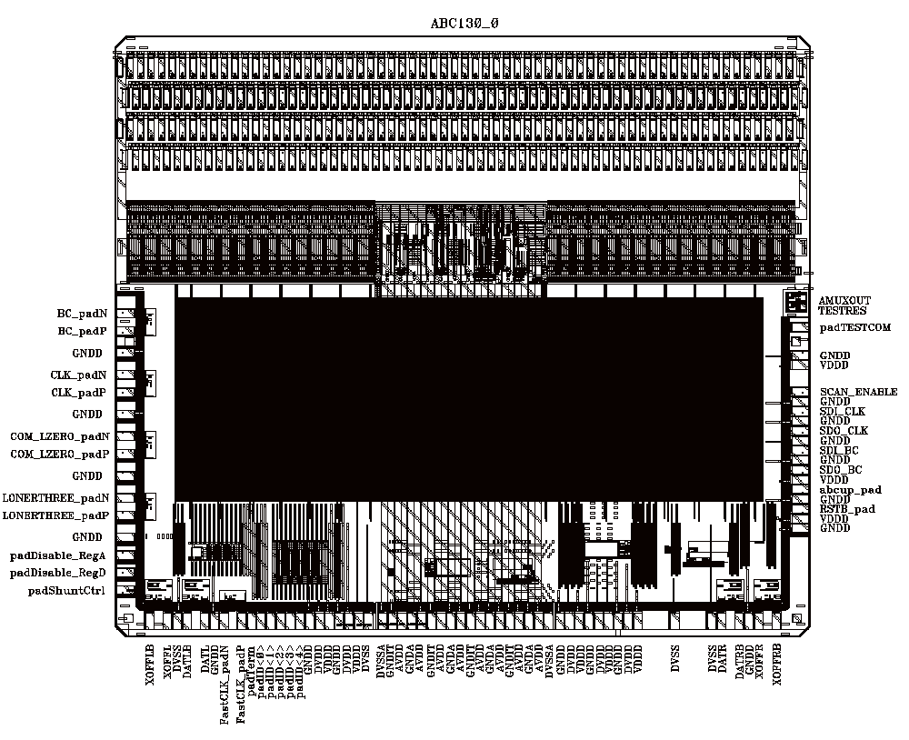
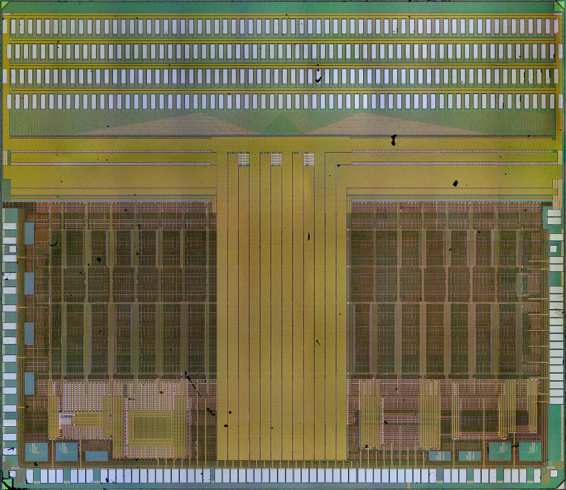
Each ABC130 chip [13] provides the initial data acquisition and readout chain for up to 256 sensor strips. Submitted in June 2013, it is the second generation of the ATLAS Strips readout family of custom Application Specific Integrated Circuits (ASICs) since the ABCD [14], which was used for the SemiConductor Tracker (SCT) readout. The ABC130 follows the ABCN-25 [15], which implemented ABCD in a new process, with some improvements, but kept a similar architecture. The ABC130 is the next member of this “ATLAS Binary Chip” family, and its suffix is from its implementation in IBM’s (now GLOBALFOUNDRIES’) CMOS8RF_DM 130nm technology. The die has a size of mm2 with the wide side meant to be oriented orthogonally to the direction of the sensor strips and along the edge of the hybrid circuit board. With these dimensions, it allows for bonding of the input pads to the sensor strip pitch, while still allowing space for decoupling capacitors to be placed between chips.
The first significant change from ABCN-25 is that the smaller feature size allowed a doubling of the number of readout channels per chip. The front-end input pads are arranged in a novel configuration of four staggered rows of 64 pads each (see figure 5(b)) for wire bonding to the AC sensor pads (see section 3.7). Ground pads at either end of each row provide for a sensor ground reference (HV decoupling and guard ring). The pitch of 119 m is chosen to allow direct bond connection from the available pad sizes to the sensor pitch. These pads are arranged so that one ASIC can be connected to two rows of strips on the sensor, with the edge of the ABC130 placed close to the boundary. The connections from both strip rows to the ASIC amplifier channels are interleaved, which provides a powerful performance cross-check in case of problems. These two rows are referred to as odd (running away from the ASIC) and even (running under the ASIC). The odd strips are also connected by long bonds that reach over the top of those for the odd strips (see figure 39). Power and signal connections are restricted to the other three sides of the die and are wire-bonded to the hybrid circuit board (see section 3.1).
Another substantial change over the ABCN-25 is in the readout system. It was substantially updated and new trigger levels have been added in order to raise the trigger rate from 100 kHz to 500 kHz, and to include the regional readout concept [5]. The new architecture has three main stages:
-
•
First, the inputs are sampled from the front-ends on every cycle of the LHC Bunch Crossing (BC) clock (40.079 MHz), and put into a synchronous pipeline (the “L0 buffer”). This allows an external process (the L0 trigger) up to 6 μs to choose which crossings to read out, with 1 BC = 25 ns;
-
•
When the L0 accept (L0A) arrives at the ABC130 (a fixed period from the original BC), the appropriate data is copied to the “L1 buffer”;
-
•
The final readout command (either R3 or L1A, described below) can then be received up to 512 μs later, and refers to a specific location in the buffer.
This architecture allows collection of data into the L1 buffer at a higher rate than the output bandwidth allows, as not all data might be selected for read out. The Regional Readout Request (R3) trigger is designed to be acted on by a small proportion of modules, selectable at the HCC-level (see section 2.2.2), based on where that module is in the detector, and provides fast readout of data that can provide input to the L1 Trigger system [5]. This proportion is expected to be no more than 10 % of the strip tracker on average. The L1A is then used to read out full information for the required BCs.
All digital signalling is carried out using SLVS[16] differential I/O between ABC130s and an HCC130 (see section 2.2.2), in a bi-directional daisy-chain fashion (see figure 6). This allows for the failure of individual ASICs as the readout direction from downstream ASICs in the chain can be reversed.

Analogue Front-End
The ABC130 analogue front-end block consists of 256 independent input channels accepting negative signals from the AC-coupled n-type strips of the ITk strips sensor. The architecture and performance of the individual front-end channels are detailed in [17]. Each channel’s preamplifier is designed around a single-ended buffered telescopic cascode with an NMOS input transistor. The input transistor is enclosed with active feedback built with a PMOS transistor biased in saturation. This feedback scheme allows for full control of the DC potential at the preamplifier output and permits the use of a very power-efficient shaper stage with a single-ended input. This particular configuration of the input stage was originally designed for the p+ on n sensors intended for the ATLAS tracker upgrade and was later modified for the negative-going signal of the current n+ on p sensor. On the ABC130, the input current from the sensor strip to the input channel modulates the transconductance of the feedback transistor and causes degradation of the noise performance and gain of that stage. Figure 48 shows a comparison of the noise performance for negative and positive signals. These issues, as well as degradation of the noise performance after irradiation, have been addressed in the new design implemented for the ABCStar [18].
The preamplifier input stage has been optimised for the value of 5 pF, covering the expected range of input capacitance of the short strip (SS) sensors, but also operates effectively with the higher capacitance of long strip sensors (LS) as well as the different end-cap sensor configurations. This includes the expected parameter variation to maximum lifetime irradiation of the modules. The inputs are protected with non-silicided NMOS thin oxide devices, whose width was chosen as a tradeoff between ESD protection and the parasitic capacitance it added to each channel ( pF). The circuit was designed to withstand a 1.5 kV Human Body Model event and a 0.6 A Transmission Line Pulse (5 ns rise time, 100 ns duration). Therefore, a series 22 resistor is used to improve response to the Charge Device Model, a tradeoff between protection and added noise. Inputs can be left unconnected without affecting the performance of any other channel.
The effective channel gain is 80 mV/fC at nominal bias currents and process parameters with a signal response peaking time of around 22 ns. The Full Width at Half Maximum (FWHM) of the response is around 35 ns and the overall shaping function is close to a second order CR-RC filter. In terms of frequency response, if the AC-coupling between booster and shaper as well as the limitation of the preamplifier bandwidth are neglected, the front-end channel can be approximated by a bandpass filter with a center frequency of about 15 MHz and a roll-off of around 20 or 40 dB/decade for frequencies below or above, respectively. The time walk of the discriminator is below 16 ns for nominal threshold settings and 50 % of a minimum ionising particle’s (MIP) signal after the total expected radiation dose.
This timing performance guarantees correct data association to a given BC for the worst case of signal charge sharing, where the charge is shared equally between neighbouring strips, and at the end of lifetime of the experiment. The response linearity is better than 5 % for signal charges from 0 to -4 fC, and better than 15 % from 0 to -8 fC. Expected noise is 850 e- for SS sensors, and 1150 e- for LS sensors. Double-pulse resolution for a -3.5 fC signal followed by a -3.5 fC signal is ns, and maximum recovery time for a -80 fC signal followed by a -3.5 fC signal is 200 ns. For a -1 fC signal, the gain sensitivity to power supply voltage is % per 100 mV. The chip features a low dropout (LDO) linear voltage regulator that, in addition to improving the rejection of power supply noise at the front-end and providing an accurate voltage to the chip independent of any voltage drops on the hybrid, allows the analogue core operating voltage to be set to within mV of the target voltage of 1.2 V. In addition, the preamplifier input transistor and feedback bias currents can be tuned to compensate for process variation with internal 5-bit Digital-to-Analogue Converters (DACs) referenced to an internal bandgap circuit ( mV).
A common threshold level is set with an on-chip 8-bit DAC and is distributed to the 256 input channel discriminators by means of current mirrors. Due to process variation, there is about 20 mV rms of threshold variance between channels, so a 5-bit TrimDAC is provided for each channel. The magnitude (range of the DAC) of this tuning can also be adjusted. In this way, the inter-channel threshold variance can be reduced into the single millivolt range (see section 3.2.6).
The output of the threshold comparators is then sampled on the rising edge of the BC clock and shifted into the L0 Buffer (FIFO). A mask register is supplied to force a zero into the pipeline and allow skipping of any noisy channels.
Each channel includes the ability, selectable by a calibration enable bit, to inject a tunable calibration pulse to simulate a strip “hit”. This capability can be used to calibrate the full tracker or a module performance on a per-strip level or as a Built-In Self-Test (BIST) function for the inputs during testing of wafers. Each channel receiving a calibration pulse is connected to a 60 fF % capacitor (10 % over full production skew) through a CMOS switch. The injected charge is defined by setting a defined voltage using an 8-bit calibration DAC. A fixed-width calibration pulse (8BC 200 ns), generated by a chip-control command, activates a chopper circuit that applies the voltage to provide a controlled amount of charge (0 to -9 fC) to the input of each channel where the calibration pulse is enabled. The polarity of the calibration pulse is also controllable by a bit in the control registers. The relative phase of the calibration pulse can be varied using a programmable strobe delay circuit from 0 to 80 ns so the position of the pulse relative to the BC can be tuned for optimal results.
Power and Ground
The ABC130 has independent digital and analogue power domains, each with its own power (DVDD and AVDD) and ground (GNDD and GNDA) pad connections, and each has its own on-chip programmable Low-DropOut (LDO) regulator that can be used to provide the required regulated V core voltage. Options were also included on the chip to allow for the application of the core voltages using external connections. By providing a sufficient number of power pads connected to the outputs of the LDOs (VDDD and VDDA) that are normally connected to decoupling capacitors, these could also safely be used as power inputs if the LDO’s input pads are not being powered. Furthermore, a voltage-controlled high current shunt circuit was included to allow for series powering of the chips. All of these modes of powering the ABC130 were tested, and it was decided to use the LDOs as voltage regulators to provide core voltages for both the analogue and digital portions of the chip when used on modules.
As part of the front-end pads array, there are four ground pads on each end to provide a ground reference for the sensor’s HV decoupling and guard ring. Furthermore, there are three special sets of ground pads: analogue ground pads specifically for the front-end (GNDIT), and one pad each for the digital and analogue ESD circuit returns. On modules, all of these are wire-bonded to the respective digital or analogue ground planes of the hybrid.
The LDOs can be controlled by programming registers: each has its own Control Enable Bit and a register field that allows them to be tuned to V in 16 steps. If the Control Enable Bit is not set, then the output voltage of the LDOs (VDDD and VDDA) applied to the chip’s core are the voltages applied to their inputs (DVDD and AVDD) minus the minimal drop across the LDOs. The chip is fully functional in this state; however, the LDOs should be tuned to 1.2 V for proper operation during data taking. In addition to the programmable control, the chip has dedicated pads that can be used to disable the LDOs in case the chip is to be powered by externally provided core voltages or using the shunt circuit. The default state on power on with no connection to the pads is to have the LDOs disabled but controllable.
The nominal pre-irradiation current at V is 40 mA for the digital portion of the chip, and 70 mA for the analogue circuitry. However, due to the Total Integrated Dose current “bump” (TID bump, see section 4.10) experienced by this CMOS technology, the amount of digital current drawn by the chip will increase by a factor with increasing radiation dose before falling back to near pre-irradiation levels as the dose moves out of the TID bump range (around 1 Mrad). To allow data taking to be consistent before, through, and beyond the TID bump operating region, the shunt circuit can be used to draw the difference between the expected maximum TID Bump current, and the current being drawn by the chip at the current TID. As the current increases through the TID Bump, the shunt current can be reduced so the overall current remains constant. Similarly, the shunt current can be increased again as the TID bump current begins to decrease, again maintaining a constant operating temperature and current draw as the TID increases, and helping to ensure comparable results for measurements taken throughout the irradiated operating regions of this CMOS technology. For the next chip generation, the ABCStar, a procedure for its pre-irradiation has been developed to pass the TID bump before the ASICs are assembled into modules. The shunt circuit is disabled by tying the Shunt Control analogue input to ground.
Digital Input and Output
There are two types of digital I/O pads on the ABC130: low-voltage single-ended CMOS I/Os for low speed signals (LVCMOS [19]), and high-speed differential SLVS I/O with a nominal 600 mV common-mode voltage and 400 mV differential voltage (SLVS [16]).
Generally, static I/O uses the low-voltage CMOS single-ended signalling, and all clocks and data I/O use high-speed differential SLVS signalling. Most LVCMOS I/O is left without wire-bonds when assembled onto a module, with the exception of the RSTB, and a 5-bit Chip ID (see section 3.1). Clock and command lines are implemented in a common-bus multi-drop configuration on the hybrids. Any command communications to the ABC130s contain a Chip ID and are only acted on by the chip whose ID matches the one in the command (with the exception that ID = 31 is a broadcast address and all ABC130s must respond to those commands). Similarly, all packets output by an ABC130 include its Chip ID to allow any packets it generates to be associated with that particular chip. Chip IDs only need be unique within a group of ABC130 ASICs read out by the same HCC.
In addition to the LVCMOS signals used during operation on a module, a number of other pads were provided as experimental features, as risk mitigation, or to assist in testing die before dicing the manufactured wafer of dice. These include:
-
•
pads to disable the digital and/or analogue LDOs (active high with CMOS pull-downs)
-
•
a Termination Enable pad (active high with a CMOS pull-down) that can be used to provide on-chip 75 (82 max.) termination for the SLVS receivers
-
•
the “abc up” pad (active high with CMOS pull-down) that can be used to invert the sense of the internal reset tree
-
•
5 pads to implement a JTAG [20] test interface (Scan_Enable, SDI_CLK, SDI_BC, SDO_CLK, and SDO_BC).
The ABC130 will operate properly with any or all of these pads left unconnected.
All dynamic operations of the chip use high-speed differential SLVS I/O (each logical signal has both a positive and negative pad to provide differential input, output, or I/O as appropriate):
-
•
two clock inputs, BC and RCLK (Readout CLocK)
-
•
two command and trigger inputs, COM_LO and L1_R3
-
•
a set of bi-directional data and flow-control signals: one set for the “left” side of the chip, DATAL and XOFFL; and one set for the “right” side of the chip, DATAR and XOFFR
The 40 MHz nominal differential BC clock is provided to all the ABC130s on a module via the HCC130 and is used to trigger sampling of the front-end inputs. The BC is also used as the clock for both the COM_L0 and L1_R3 differential Dual-Data Rate (DDR) inputs with effective input data rates of 2 times BC (80 Mbps nominal). Each input is split into two 40 Mbps signals. On the rising edge of BC, the COM_L0 is latched as the command data stream to the ABC130s; and on the falling edge of BC, that signal is latched as the L0 trigger. Similarly, the L1 trigger data stream on L1_R3 is latched on the rising edge of BC, and the R3 trigger data stream is latched on the falling edge of BC. Finally, the HCC130 provides the differential RCLK signal at up to four times the rate of the BC (160 MHz nominal) that is used to clock data on the DATAL/R digital readout pads and the XOFFL/R flow-control pad signals.
The bi-directional signals are configured in pairs, so that when DATAL is an output, DATAR is an input and vice versa. Similarly when DATAL is an output, XOFFL is an input and vice versa as in table 1. A single configuration register bit determines whether the ABC130 is operating in a “right to left” mode or in a “left to right” mode. When configured as outputs, the differential output current of the drivers are programmable between 1 mA and 7 mA, in 8 steps.
| Signal | Side of ASIC | I/O in L-R | I/O in R-L |
|---|---|---|---|
| DATAL | Left | Input | Output |
| DATAR | Right | Output | Input |
| XOFFL | Left | Output | Input |
| XOFFR | Right | Input | Output |
When in “right to left” mode, DATAR is an input and forwards data received from its neighbour to the right through to DATAL. XOFFL is an input (recieving flow-control signalling from its neighbour to the left) and XOFFR is an output (providing flow-control to its neighbour to the right). When in “left to right” mode, the data, flow-control, and I/O directions are reversed. The ABC130s on a module are connected in a daisy-chain with the DATAR and XOFFR on one chip connected to the DATAL and XOFFL of the next chip to its “right”. The farthest “left” and farthest “right” ends of the daisy-chain are connected to the HCC130 (see section 2.2.2), which can receive data and/or provide flow-control signals from either of the ends of the daisy-chain. This architecture allows part of the daisy-chain to be configured as “left to right” and the other part as “right to left” to handle the case of a single failed ABC130 anywhere in the daisy-chain. All chips to the “left” of a faulty ABC130, if any, are configured in the “right to left” direction; and all chips to its “right”, if any, are configured in the “left to right” direction. This way, maximal physics data can be read out from a partially operational module (see figure 6).
The ABC130 was manufactured on a Multi-Project Wafer (MPW) run along with an unrelated chip. There were two different versions of the ABC130 in each reticle on the wafer: the ABC130_0 and the ABC130_1, which were identical in function except the ABC130_1 additionally had experimental circuitry for a Fast Cluster Finder (FCF) and additional pads to support that functionality. The FCF was designed to provide prompt, BC-synchronous, cluster position data to an external device that could be used to correlate clusters between tracking layers and select high (transverse momentum) coincidences to a trigger processing unit. Ultimately, this functionality was not used on the modules built with ABC130 chips, and was not tested during wafer testing either. The operation of this circuitry is beyond the scope of this article, but can be found in the ABC130 Specification [13].
Chip operation
For normal operation, after the chip is reset, the registers on each ABC130 are initialised using the command stream of the COM_L0 DDR input with the values that have been determined to provide it with nominally tuned settings, and to set all relevant mode bits necessary to put the chip into the desired operational configuration. These settings include:
-
•
the LDO tuning value required to provide 1.2 V core voltages to the analogue and digital circuit domains
-
•
all of the front-end control DACs and TrimDACs to correct for process and inter-channel variation
-
•
the channel mask registers to disable any known faulty input channels
-
•
the required SLVS driver currents
-
•
and the threshold value.
Setting the threshold to an optimal value for each ABC130 - which is distributed to all of its 256 input channels, each of which is fine-tuned by the per-channel TrimDACs - is critical, as it determines the front-end’s sensitivity to signals from the sensor strips it is reading out, and its susceptibility to noise from the sensor and the front-end circuitry. The threshold can be set based on the requirements of a particular data-taking session and determines the “hit” rate (which can include both signal and noise), and thus the maximum data transmission bandwidth from the module during operation. There are features that can limit the maximum data rate of the ABC130s, but using these results in the discarding of potential hits (see below).
The decision to record a hit or no-hit is taken on the rising edge of the BC clock. The state of all 256 input channels of every ABC130 on a module will be sampled into its L0 Buffer, a 256 bit-deep FIFO. The state is formed by the logical AND of the input comparators reading out the sensor strip it is wire-bonded to, and the inverse of the associated Mask Registers bits (a 1 bit in a Mask Register will force its associated channel to always read as the 0, or “no hit”, state). Each of these 256-bit input vectors is pushed from the front-end onto the L0 Buffer FIFO along with the value of an 8-bit, command resettable, BC counter (BCID). Because this process is continuous, a sample will remain in the L0 Buffer to be read out for a maximum of 6.387 s before falling off the far end of the FIFO.
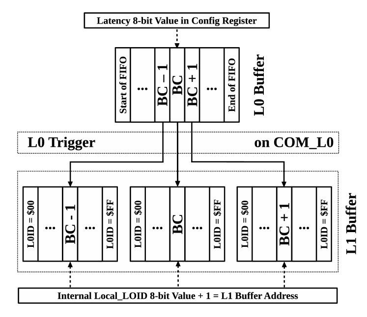
The next step is to capture the data from the L0 buffer into the L1 buffer. To save input vectors for possible later readout, an L0 (first level) trigger accept needs to be issued. This L0A is actioned by logic-level 1 on the COM_L0 DDR input. When an L0A is received, one “event” from the L0 Buffer is transferred to the L1 Buffer. The Latency is the fixed number of BCs between when the front-end is sampled and when an L0A is received by the module from the trigger system to store that sample. This is configurable by the setting of the 8-bit Latency value in the chip’s control register set, and specifies the address in the L0 Buffer of the centre of a 3-BC long “event”. As shown in figure 7, an entry in the L1 Buffer consists of three 256-bit memory blocks, which will be used to store the L0 Buffer entries for: the previous bunch crossing, the bunch crossing of interest, and the next bunch crossing. All three of the values copied to the L1 Buffer (both the 256-bit input vector and the associated 8-bit BCID) will further be tagged with an 8-bit Local L0 IDentifier Counter (Local_L0ID Counter) value. This whole event is stored at the address in the L1 Buffer specified by the Local_L0ID Counter after it is incremented by one. Like the BC Counter, the Local_L0ID Counter is settable to a known initial value (usually $FF) when data taking begins so both the trigger system and the ABC130s are in synchronization and the first L0 Trigger writes into location 0 of the L1 Buffer. Since the L1 Buffer can store 256 entries, for a 500 kHz L0 Trigger rate, for example, it can hold the data for an event for 512 s before it is overwritten with another event.
The final stage is to read out the event data from the L1 buffer. To read out the physics data of an event, an L1 or R3 Trigger is issued by the trigger system via the L1_R3 DDR input (through the HCC130). Each of the trigger commands consists of a three-bit header - 110 for L1 and 101 for R3 - followed by the 8-bit L0ID value of the event to read out. The L0ID value sent with the trigger is simply the number of L0As sent since the Local_L0ID counter was reset, and corresponds to the memory address of the L1 Buffer that will be read out. Depending on whether an L1 or R3 Trigger was issued, the event is sent to the L1-DCL (Data Compression Logic), or the R3-DCL, which generate a sequence of fixed length data packets.
The R3-DCL produces only a single output packet, and is intended to provide a quick snapshot of whether or not any clusters were detected for a particular bunch crossing event. Conversely, the L1-DCL produces a comprehensive output of all cluster data for the relevant event where the hit data matches a specified pattern, and can result in many packets being queued for transmission. Both DCLs find clusters of hits, by searching the channels first in one set of 128 channels followed by the other 128 channels. Thus clusters are found only between strips in the same sensor region. Also, it does not “wrap” from one set to another. These are recorded in the output packet as 0-127 and 128-255.
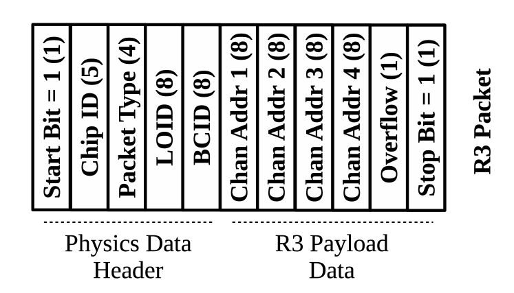
For an R3 Trigger, the R3-DCL will generate a single output packet flagging whether there are no hits, some hits (1-4), or many hits (more than 4). The R3-DCL can be configured through the “EN_01” bit in the configuration registers to either define a “hit” by looking for a hit only in the L1 Buffer block corresponding to the selected BC (level mode), or to look for a level change from 0 to 1 between the previous BC and the selected input vector (edge mode). The R3-DCL only registers clusters that have hits in a maximum of three channels, larger clusters are ignored. The location of the first hit is reported for clusters with width of 1 or 2, and the location of the central strip when the cluster width is 3. The R3-DCL will report the locations of a maximum of 4 hit clusters per event, and will set an overflow bit in the output packet if there are more than 4 valid clusters [13]. The format of the R3 packet is detailed in figure 8.
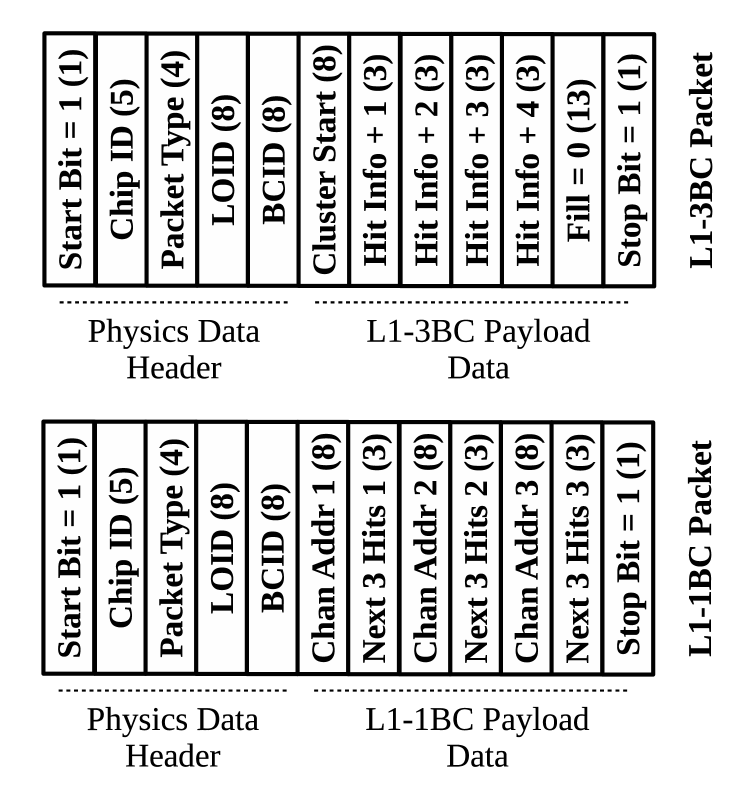
For an L1 Trigger, the L1-DCL reports clusters in one of two formats as selected by the “mcluster” bit in the configuration registers: either L1-3BC mode where information on all 3 recorded BCs are reported; or L1-1BC mode, where only cluster patterns are reported (see figure 9). For both modes, a compression mode can be configured to choose which clusters to report based on the pattern of bits in the 3 recorded BCs. There are two patterns for use during normal data taking, X1X (level) and 01X (edge), where the X indicates “don’t care”. A further “any hit” mode to be used for detector alignment matches (1XX or X1X or XX1). A final XXX mode is intended only for chip testing. Clusters are scanned for in the two sets of 128 channels based on this mode and clusters formed. When a hit is found that matches the selected pattern, that bit forms the first bit of that cluster and its location is used to report the start of the cluster in the packet. For the L1-3BC mode, that location is used as the channel address reported in the packet. The address is followed by the 3 bits for the hit on that channel (from the 3 recorded BCs), and the next three channels(whether or not they have any hits in them). The DCL then moves to the following channel to check for a new cluster start. Because 4 channels are reported per L1-3BC packet, a total of 64 packets could potentially be created if at least every 4th channel had a hit to cause a cluster to be reported. For the L1-1BC mode, up to three clusters can be reported: each one comprised of the 8-bit cluster start location, and the one-bit hit status of the following three channels (3 bits) based on whether that channel matched the hit criteria. Like the L1-3BC mode, the next cluster is searched for after the last bit of the previously reported 4 channels of cluster data. Because 3 clusters can be reported in each packet, up to 22 L1-1BC packets could be generated if every 4th channel had a hit to cause a cluster to be reported. It should be noted that due to the potentially large number of packets generated for an L1 Trigger event with many hits, the possibility of saturating the front-end circuitry with noise or hits from the sensors when the thresholds are set low needs to be managed carefully. If a large number of hits are expected, the L1 Trigger rate needs to be controlled carefully to ensure no loss of data in those situations. A further feature is provided in the ABC130 that allows the number of packets generated to be capped at some specified number less than 64 for L1-3BC mode or 32 for L1-1BC mode. While this mode could result in data loss, the assumption would be that the high-occupancy data is not useful.
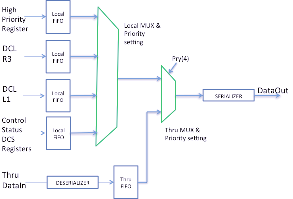
As packets are created by the DCL, they are pushed onto the appropriate flow-controlled FIFOs and are then pulled from the FIFOs and serialized according to their relative priority. In addition to FIFOs for the L1-DCL and R3-DCL, there is a FIFO to queue configuration register reads, and a separate FIFO to output the reading of a special high-priority status register (Register $3F). These are output in order of highest to lowest priority: high-priority register reads, R3-DCL, L1-DCL, and then regular register reads at the lowest priority. Furthermore, packets that are being transmitted through the ABC130 from an adjoining ABC130 or HCC130 are interleaved into the output data stream based on the setting of 4 Pry (priority) bits in the configuration registers. If there are packets from the internal data sources to send, Pry sets the number of through-packets that might be forwarded before one internally generated packet needs to be sent. Thus, if Pry is set to 0, then a through-packet will always be sent before any internally generated packets. If Pry is set to 8, for example, then 8 through packets (if present) will be forwarded before sending the next internally generated packet. If the through-packet FIFO (which is 4 deep) is about to be filled, the XOFF signal is asserted to the upstream chip to prevent the FIFO from overfilling and for through-packets to be lost that way. Similarly, if the internal FIFOs are about to fill up, the blocks that are sending data to them receive internal flow-control signalling and must stop operation until FIFO space is available for them to continue sending (see figure 10 on the FIFO and priority structure).
Wafer testing
Since ATLAS ITk strip tracker modules have up to 12 ABC-style chips connected to one HCC, if even one chip were to fail due to a manufacturing defect during module testing, it would require a risky and complex re-work effort to attempt to recover the module. While the data-flow architecture allows for the routing of data around a failed ABC130, 256-channels of data would still be lost. If that repair process failed or damaged the module, that one failed chip could result in the costly loss of an entire hybrid or module. As such, each ABC130 die undergoes an extensive testing and characterization process while still on the wafer using specialized wafer probing equipment and custom software. The ABC130s on the wafer are categorized into good (grade A), usable in the lab or in the event of a parts shortage (grade B), and bad dice (which can be used as mechanical samples for assembly testing and tooling development).
ABC130 wafer testing was conceptualised, developed, and implemented using a commercial semi-automated wafer-probing system, a commercially manufactured custom probe card, a custom interface card and a commercial off-the-shelf (COTS) FPGA development board. The use of COTS components resulted in a much faster test system development compared to the custom electronics used for wafer testing during the construction of the ATLAS Semiconductor Tracker [21]. The wafer test software was integrated with the module test software suite: the ITk Strips DAQ (ITSDAQ, formerly SCTDAQ), see section 3.2.5. In the tests run on each ABC130 die on every wafer, the wafer is manually placed on the wafer-probing station’s platen and positioned using the probe-station’s microscope’s digital camera. Once the wafer is aligned, the wafer test software can step automatically between each of the ABC130s on the wafer and run all necessary tests on it.
The tests begin with basic integrity testing looking for gross failures of the die in terms of power supply currents and to ensure proper contact between the probe card and all of the die’s pads. The tests then conduct a number of further sanity checks including:
-
•
setting registers to default values and verifying that the power supply currents change appropriately
-
•
tuning the chip’s LDOs and front-end DACs
-
•
scanning all other DACs
-
•
a series of digital tests to check the functioning of the digital portion of the chip
-
•
a series of complex functional tests are conducted to verify the chip’s proper operation from front-end to data output
These final tests include tuning the chip’s strobe delay value to provide optimal stimulus using the built-in calibration pulses, and then running a comprehensive 3-point gain test where each channel’s front-end response to three different calibration pulse charges (0.5 fC, 1.0 fC, and 1.5 fC) is plotted to determine the gain response and noise level of all the input channels (see section 3.2.6). These tests also verify the functioning of triggering blocks, the L0 and L1 Buffers, the cluster finding and sparsification blocks, and the data transmission I/O blocks. The data is analysed in real time by ITSDAQ and the parts undergo a preliminary categorisation at that phase. Further analysis is performed offline on the data produced by the wafer probing routines where comparative analyses are also done between dice and between wafers, and the die categorisation can be updated as needed at that phase.
In preparation for the next generation chip, the ABCStar, and to ramp up towards full production testing, a second wafer test site was established. Whereas previously a system primarily developed in-house had been used for wafer testing, the second test site was established at an outside company to use their commercial, fully automated, wafer-probing stations and associated industrial test software infrastructure.
2.2.2 HCC130
The Hybrid Chip Controller, HCC130, the first ATLAS strips prototype chip controller, was submitted for fabrication in August 2014. The 99-pad mm2 ASIC (see figure 11) was designed to provide the interface between the hybrid-mounted front-end ABC130 and the off detector electronics through the GBTx [22] using LVDS-like low voltage differential drivers and receivers. It also contained an early version of the Autonomous Monitor that was functionally validated and eventually moved to the AMAC ASIC (see section 2.2.3). HCC130 receives the 40 MHz bunch crossing (BC) clock and two, custom protocol control signals from multi-drop buses driven by the GBTx. Both of these control signals are encoded with two independent logical streams time multiplexed into one. Data of all types sent from each module are transmitted point to point by the HCC130 to the GBTx at 160 or 320 Mbps.

The L0_COM physical control signal encodes L0, a beam synchronous trigger that stores the ABC130 pipeline delayed data into a 256-word deep data buffer from which data are requested for readout. The second logical channel of L0_COM signal is a priority based variable length Command (COM) protocol that provides control to set operational modes in both the HCC130 and ABC130 ASICs and initiates requests for data from internal registers in the HCC130 and ABC130 ASICs. The difference in naming from the ABC130 indicates a subtle difference in that the HCC130 modifies the COM signal before forwarding to the ABC130, to mask out commands intended for ABC130 attached to other HCC130 on the same bus.
The R3s_L1 physical signal provides two triggers used to request readout of data from the ABC130. The L1 is broadcast directly to the ABC130s, requesting readout of data from one of the 256 memory locations of the ABC130s L1 buffer. In addition to the L0ID identifying the memory location to read out, the R3s signal contains an extra 14 bits, used to propagate the signal only to HCC130s with matching addresses. In this mode only addresses 2-29 are available. If the address matches, the mask bits are stripped and the remainder broadcast to the ABC130s.
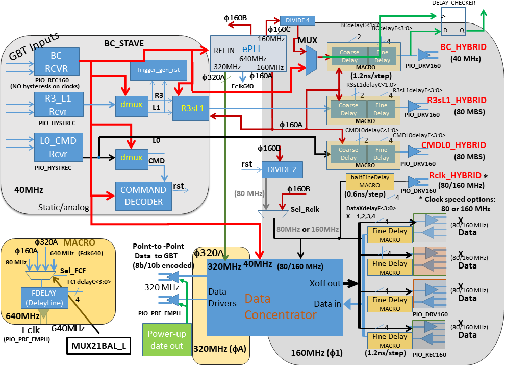
The HCC130 utilises a copy of the CERN ePll block designed for the GBTx [22] to generate low jitter, 40, 80, 160 and 320 MHz clocks using the incoming multi-drop 40 MHz BC as a reference. The ePll is used internally on the HCC130 and provides the hybrid ABC130s with a regenerated, programmable, phase delayed 40 MHz clock for phasing event data properly within the beam crossings and related pipeline control. It also provides the ABC130s on the hybrid with a selectable 80 or 160 MHz data clock to drive the serial loops used for data readout. HCC130 can collect data from the hybrid through any of its four serial receivers attached to either end of the two hybrid readout loops. Corresponding XOFF signals allow for flow-control to the ABC130s. This readout technique provides contingency for single and multiple chip failures in either of the two ABC130 serial data loops. Once on the HCC130, a priority encoder ensures an even flow of data from the two ends of each loop and that R3 data are sent to the DAQ system with the highest priority. A data concentrator merges data from the two loops. A detailed HCC130 functional block description is shown in figure 12.
2.2.3 AMACv1a
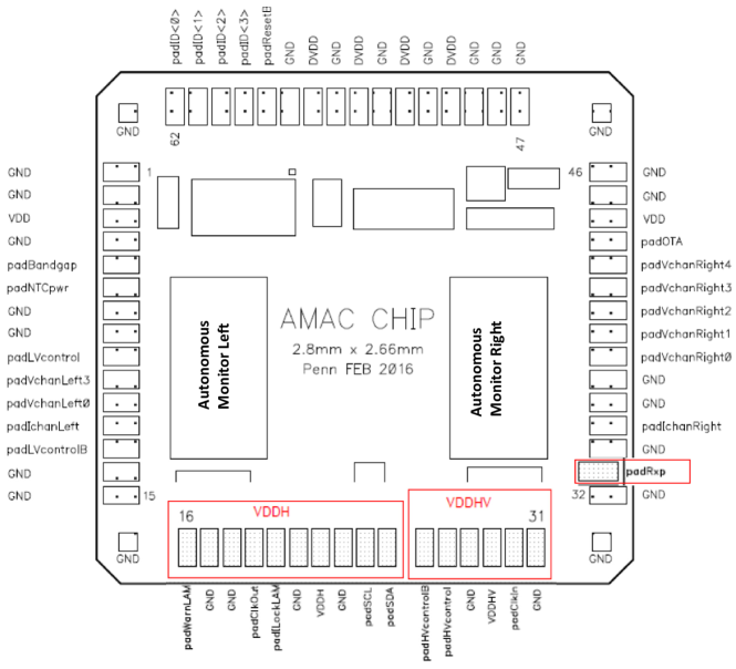
The Autonomous Monitoring And Control ASIC (AMAC) was submitted for fabrication in August 2016. It was the first successful prototype of the radiation tolerant, ten bit precision analogue monitor ASIC and was constructed using two identical seven channel Autonomous Monitor blocks originally housed in the HCC130. The AMACV1a pad frame is shown in figure 13: it has 62 bond pads and a die size of mm2. An internal ring oscillator provides a near 40 MHz clock to control the autonomous monitor functions and I2C protocol is used for control and readout. AMACV1a monitors 14 independent module level parameters: voltages, temperatures and sensor leakage current. A clock driven state machine controls a switched capacitor stepped integration ramp to create a common reference for the Wilkinson style ADC. Each integration step increases the reference by 1 mV and increments a ten bit counter reset to 0, each 1023 step ramp cycle. Each of the 14 monitored parameters is translated into a voltage between 0 and 1 V and compared with the ramp that covers the same range. When the reference ramp exceeds the value of the measured parameter for two consecutive ramp steps the counter value is recorded in a register and compared with pre-programmed upper and lower limits. Out of limit values are flagged and - if enabled - can switch the state of four logic outputs outputs that may be wired to LV or HV supply controls. Measured values are updated and stored locally once per millisecond. They may be readout remotely through the I2C interface.
2.3 Hybrids
Readout chips for ABC130 barrel modules are mounted on flexible, radiation hard and low mass Polyimide circuits (called hybrids), which were developed to carry ten ABC130 readout chips and one HCC130 readout chip each (see section 2).
Hybrids provide the following electrical functionalities:
-
•
Multi-drop external clock and control are connected to the hybrid
-
•
On-hybrid internal clock and control are distributed to the ABC130 chips
-
•
All ASICs on the hybrid are connected to a common ground and power domain
-
•
Hybrid front-end data is returned to the high-level readout via the end-of-substructure card (see figure 1(a))
The hybrid readout topology groups the ten ABC130 readout chips into two daisy-chains of five chips each. Each chain can be read out in either direction by the HCC.
ABC130 barrel modules are assembled by gluing hybrids with readout chips directly onto the surface of silicon strip sensors (see section 3.7). The circuit layout has been optimised to minimise electrical interference into the sensitive analogue front-end electronics or sensor strips. This has been achieved by the use of a single power and return domain with partioning of analogue and digital circuitry to mitigate common impedance coupling of the analogue and digital signalling. Furthermore, fast digital signalling within close proximity of the analogue front-end are routed as differential strip-lines to take advantage of the shielding effect of the return planes.
In addition to ABC130 and HCC130 readout chips, hybrids are equipped with two NTC thermistors, of which one is used to monitor the hybrid temperature during operation. The second one is part of a temperature interlock system required during the burn-in of hybrids as part of their quality control.
In order to ensure a maximum yield, hybrids were designed to utilise standard manufacturing processes with long-term reliability. Tracks and gap sizes are about , vias (plated laser drilled holes) have a hole diameter of about and lands of , which ensures uniform plating and therefore reliable contacts through vias. Barrel hybrids comprise three copper layers ( thickness) between polyimide dielectrics ( layer thickness), resulting in a total hybrid thickness of approximately .
Hybrids are produced on panels (glass-reinforced epoxy laminate sheets) which hold four X- and four Y-type hybrids (see figure 14) as well as two test coupons per panel, which are used for hybrid manufacturing quality control:
-
•
testing of via reliability by via chain resistance measurements
-
•
monitoring trace etching quality by testing DC resistance of test traces
-
•
testing quality of surfaces for wire bonding by performing wire bonding pull tests
Hybrid panels are equipped with vacuum holes and landing pads for assembling hybrids and readout chips (see section 3.1) as well as traces and connectors for the electrical testing of fully assembled hybrids (see section 3.3).
2.4 Powerboard
The powerboard fulfils three purposes on the ITk Strip Module:
-
1.
DCDC regulation of the 11 V input to 1.5 V to supply the ASICs on the hybrid
-
2.
High-voltage switching of up to -500 V to reverse bias the sensor
-
3.
Control of low-voltage and high-voltage supply, as well as monitoring of voltages, currents, and temperatures
The DCDC regulation is achieved by the FEAST chip [23], a radiation hard custom ASIC developed by the CERN electronics group for various experiments and their detectors. The FEAST employs a buck-converter style switching regulator, which requires an external inductance. For the powerboard, this inductance is an air-core solenoid coil with a nominal inductance of 545 nH and DC resistance of 35 m. It is required to be an air-core coil as the detector will be placed in a 2 T solenoid field, which precludes the application of ferrite cores.
Due to the shape and characteristics of an air-core solenoid, during operation the coil emits RF noise, which could be picked up by the silicon strips underneath and around the powerboard. Therefore, the whole DCDC circuit is enclosed by a shield formed by a specific copper layer in the PCB underneath and a 100 m thick aluminium shield-box soldered on top with continuous seams.
Switching control of the high-voltage is gained via a GaNFET
transistor switch, by routing the high-voltage supplied to a module
onto the powerboard through the switch. This routing also allows a
low-pass RC-filter to be placed at the output of the high-voltage line,
which is connected to the silicon sensor. To switch the GaNFET, a
voltage of more than 2 V between gate and source is needed, as the
source of the transistor after closing the circuit is at high voltage. An AC signal at a frequency of 100 kHz and amplitude of
3.3 V is AC-coupled into the high-voltage domain. It is then amplified
and rectified via a quadruple charge pump circuit, which generates the
necessary gate voltage with respect to the current source potential.
Both the low-voltage and high-voltage domain are controlled by the AMAC chip, which has been designed specifically for the usage on the powerboard. It can generate an enable signal for the FEAST chip to turn on the power to the 1.5 V domain and also generates the AC signal to switch the high-voltage on or off. Furthermore, the AMAC chip features multi-channel ADCs to measure multiple operation critical values:
-
•
input and output voltage and current
-
•
FEAST internal temperature (via an internal PTAT circuit)
-
•
powerboard temperature (via NTC thermistors)
-
•
hybrid temperature (via NTC thermistors, for later powerboard versions)
-
•
and silicon sensor leakage current
It also contains logic to set an upper and lower boundary on the monitored values and if these limits are violated it can interlock the low-voltage or high-voltage of the module.
A picture of powerboard v2 can be seen in figure 15, which shows the main components of the powerboard. On this specific version of the powerboard the AMAC is powered via two commercial linear regulators, in the next version of the powerboard these will be replaced by a rad-hard linear regulator, the LinPOL12V, which will also be used in the final production version of the powerboard.
3 Module construction
Each ABC130 barrel module consists of one sensor (see section 2.1), one or two hybrids (see section 2.3) with ten ABC130 chips and one HCC130 chip each (see section 2.2) and one powerboard (see section 2.4). Modules are assembled in a defined series of steps optimised for early defect detection to avoid the use of low-grade electronics on good quality sensors:
- 1.
-
2.
electrical connection of readout chips to hybrids and powerboards using an automated wire bonding process
- 3.
-
4.
gluing tested hybrid(s) to sensor (see section 3.7)
-
5.
electrical connection of hybrid(s) and sensor using an automated wire bonding process
-
6.
electrical tests of module (see section 3.8)
-
7.
gluing tested powerboard to sensor (see section 3.7)
-
8.
electrical tests of module (see section 3.8)
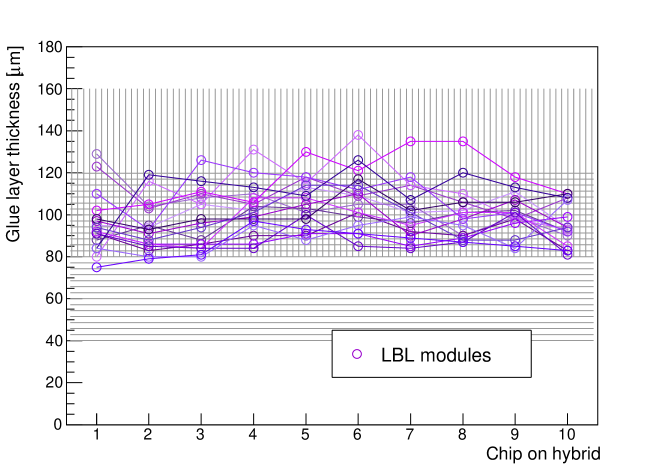
Components are mechanically and thermally connected using adhesives, which achieves the low material budget required in the ATLAS tracker [5]. Each hybrid and module is assembled in a manual process using custom designed precision tooling (see section 3.1) including a stencil to ensure a reliable glue coverage and thickness between components. After each gluing step, the glue thickness between components is checked by performing metrology measurements. Since the stenciling process ensured a consistent glue volume, glue layer thicknesses outside the specified range were found to lead to lower quality wire bonds:
-
•
thick glue layers, corresponding to low glue coverage under components, resulted in insufficiently supported bond pads and therefore weak wire bonds
-
•
thin glue layers led to glue covering wire bond pads and prevented electrical connections between bond pads and attached wire bonds and thereby caused electrical failures
Additionally, glue layers with insufficient height between hybrids or powerboards and sensors led to glue spreading towards the sensor guard ring area, which was found to result in early sensor breakdowns [24].
3.1 Hybrid assembly
For the construction of hybrids, ten ABC130 readout chips and one HCC130 readout chip are glued onto an X- or Y-type flex in a series of manual steps that use precision tooling for positioning.
Prior to assembly, the involved components were tested for electrical functionality:
-
•
circuits on the flex were tested by the manufacturer
-
•
ABC130 ASICs were probed on a full wafer of chips (see section 2.2.1)
-
•
most HCC130 ASICs were probed, but after a high success rate during initial tests (97 %) and technical difficulties with the test setup, tests of individual ASICs were eventually stopped
All components were handled in a cleanroom environment using vacuum tools to avoid contaminations prior to wirebonding (see below).
In order to be populated with ASICs, a panel with hybrid flexes was positioned on a vacuum chuck with vacuum holes under each hybrid flex. Vacuum was applied in order to flatten hybrid flexes and provide controlled glue heights between ASICs and hybrids. Positions of ASICs on hybrids were controlled using matching positions of precision holes and locating pins in the assembly tooling (see figure 16).
ASICs were first positioned in a dedicated chip tray with cutouts for each ABC130 ASIC (see figure 17), which aligned each ASIC with respect to locating holes matching those in hybrid panels. ASICs were picked up using a vacuum pick-up tool (see figure 18) with individual vacuum pedestals for each ABC130 chip and locating pins to align the tool in the chip tray.
Barrel pick-up tools were designed to be height-adjustable: each landing foot consisted of a precision metal sphere glued into a fine thread screw which could be adjusted to increase or reduce the height of the pick-up tool over a hybrid or sensor. Contact measurements of adjusted pick-up tools showed that landing feet achieved height settings with respect to ASIC pickup areas of up to 10-20 m, in addition to a required ASIC pickup area flatness of .
In order to implement a continuous assembly and testing process for hybrids, a UV cure epoxy (Loctite 3525) was chosen after a study of several alternatives [25]. It replaced the previously used silver epoxy (Tra-Duct 2902). The UV cure epoxy was dispensed on each landing pad on the hybrid using an automated glue dispenser: a combined volume of 2.0 mg was dispensed in a five-dot pattern matching position indicators on each landing pad (see figure 16) with 0.4 mg per glue dot. After dispensing the glue, the pick-up tool holding ASICs was placed on top of the hybrid.
The intended glue height between flexes and ASICs was achieved by constructing dedicated landing feet on the pick-up tool to a height that, when placed on the landing pads of the hybrid panel, would ensure the required gap between ASICs and hybrid surface. The target glue thickness for this gluing step was 80 40 m at the beginning of the project, but was later increased to 120 40 m, which was found to produce more reliable results.
A brass weight was placed on top of the pick-up tool to ensure a good contact of the landing feet on the panel. Afterwards, UV LEDs (Edison Opto Federal 3535 UV Series [26]) were placed next to the hybrid to shine UV light into the gap between ASICs and hybrid for 10 min, which was found to be sufficient to fully cure the glue underneath each ASIC.
For historic reasons (the HCC chip equivalent from the ABCN-25 chip set was not mounted on hybrids [3], but on module test frames), ASIC pick-up tools for the ABC130 chip set did not include a vacuum pick-up area for the HCC130 chip. Therefore, HCC130 ASICs were glued onto hybrid flexes without dedicated tooling and placed by hand. For this gluing step, a silver-filled epoxy glue (Tra-Duct 2902) was used, as its higher viscosity facilitated the manual assembly process.
After each hybrid assembly, the height of each ASIC was measured to track the achieved glue height and reliability of the gluing process. Figure 19 shows height measurement results for a range of hybrids: all hybrids were found to have glue thicknesses within the specified allowed range, well within the allowed uncertainties.
After populating a hybrid with ASICs, each ASIC is electrically connected to the hybrid using wire bonding: a 25 m aluminium wire (with 1 % silicon content) is fed through a bond wedge, pressed down on the ASIC pad with a force while simultaneously applying ultrasonic vibrations and thereby welding the wire to the metal pad underneath. Using the same process, the bond wire is afterwards attached to an electroless nickel immersion gold (ENIG) plated pad on the hybrid side and cut off. Figure 20 shows the wire bonding scheme for wire bonds between ASIC and hybrid (back-end bonds).
Wire bonds are placed using a program that contains position information, loop shapes and bonding parameters for all wire bonds on the hybrid. Prior to using the program on a hybrid, it is aligned to the positions on hybrid and chips using fiducials (see figure 20).
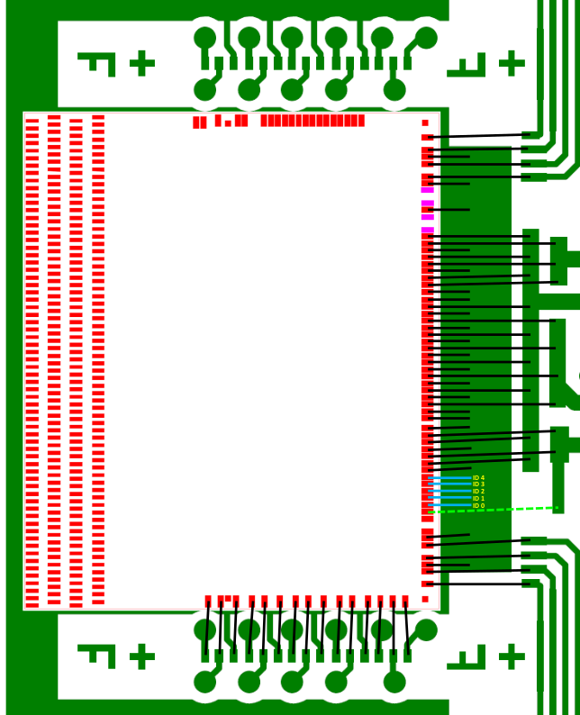
In order to read out ten identical ABC130 chips per HCC130 and two HCC130 chips on a short strip module, each ASIC is assigned an individual ID number using bond pads on dedicated address fields. Figure 21 shows the wire bonding scheme for an HCC130 ASIC with its address field.
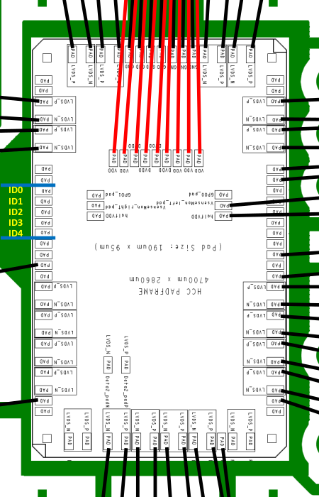
In order to assign an ID number to a chip, bond pads on the address field are connected to a hybrid ground pad using wire bonds. Address fields consist of several numbered fields (e.g. ID0 to ID4 on an HCC), where each field corresponds to a binary digit (i.e. to on an HCC). If a bond wire is attached to an address field bond pad, the corresponding number is set to 0. The five ID pads on an HCC130 therefore allow to assign ID numbers from 0 to 31. Ten ABC130 chips on the same hybrid are assigned IDs 16 to 25 sequentially, while HCC130 ID numbers can be assigned randomly, as long as HCC130 IDs on groups of 13 or 14 modules, i.e. up to 28 HCC130 chips, read out together are unique to each HCC130.
The wire bonding process is performed with the hybrid being located in the panel where it was manufactured. During wire bonding, the hybrids are held in place and flattened by applying vacuum to the hybrid backplane.
3.2 Electrical tests of hybrids and modules
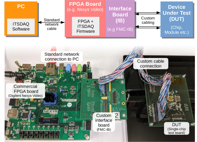
3.2.1 Physical DAQ system
ABC130 objects are controlled and read out using ITSDAQ. The ITSDAQ system comprises a PC running a software component and FPGA-based hardware to handle the digital logic interfaces and time-critical functions. Commercial hardware and standards-based protocols are used wherever possible; this reduces cost, and also complexity in some cases. The connection from the PC to the FPGA is via standard Ethernet. Custom interface boards are manufactured to match the various ASIC and module connector configurations, and these are plugged into the FPGA-board via (standards based) connectors provided; most commonly an FPGA Mezzanine Connecter (FMC) and Digilent’s VHDCI based standard: VMOD.
For the FPGA hardware, commercial educator-focused “development” boards have been selected as these are relatively low cost, widely available and have a product lifetime of many years. The Digilent Atlys [27] and Digilent Nexys Video [28] have been used widely. The custom electronics needed to connect the development boards to ABC130-based objects take the form of “Interface-Boards”. By using a range of Interface-Boards a common FPGA-board is adapted to the wide range objects under test.
Figure 22 shows a block diagram of the DAQ functional components, along with an example of a real setup (without the PC).
3.2.2 PC/firmware interface
Communication with ITSDAQ hardware is via blocks of data transferred in network packets. Initially raw Ethernet was used, but this has been superceded by the UDP/IP protocol as it allows easier management of the interface. It has been found to be sufficiently reliable on point-to-point links. The same packet format is used in both directions.
ITSDAQ network packets contain one or more opcode-blocks (“opcodes”) formatted using a custom protocol. Table 2 shows the opcode wrapper protocol that forms the payload portion of UDP packets. In the raw-Ethernet case, the first field (magic number) is used as the standard Ethernet Type value (effectively defining a new type of packet) and the rest is the payload. A sequence number is provided to track packet loss. The Opcode sub-system is detailed in section 3.2.4.
| Field | Size | Description |
|---|---|---|
| Magic number | 16 bit | 0x876n. In raw-Ethernet mode |
| this becomes the Type field | ||
| Sequence number | 16 bit | Defined at source. Software can use anything, |
| firmware uses a counter | ||
| Packet length | 16 bit | Length in bytes of entire packet, |
| including trailer (CRC) | ||
| Opcode count | 16 bit | Number of opcodes in the packet |
| Opcode 0 | ||
| … | ||
| Opcode n | ||
| … | ||
| Trailer | 16 bit | CRC |
Debugging communication (and operation) can be aided using Wireshark software, especially if using the ITSDAQ protocol dissector provided with ITSDAQ software.
3.2.3 Firmware structure
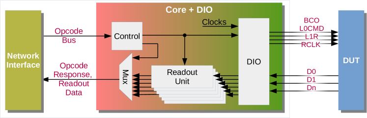
The firmware needs to be compatible with multiple FPGAs, networking chip sets, board-clock frequencies and devices under test. The firmware is structured to cope with variations in board layout, FPGA family and the devices under test. To aid this, the firmware is split into 3 distinct parts (see also figure 23):
-
•
Network + Clocks: FPGA board specific; Interfaces to whatever network chip set is supplied on the board, and generates 40 MHz and related clocks from the local oscillator.
-
•
Main/Core: Generic; FPGA and device agnostic, the same code is used for all builds (but does have compile time options).
-
•
DIO: specific to FPGA, Interface Board and device under test (DUT); Handles physical connections (pinout of interface board, physical IO types – LVDS, CMOS, pullups etc. and FPGA primitives – ISERDES, IODELAY2 etc.)
The core firmware provides many functions, including: control signal encode, front-end data-format decoder, histogrammer, sequencer, trigger generation (oscillator, random, structured bursts), I2C and other slow interface controllers.
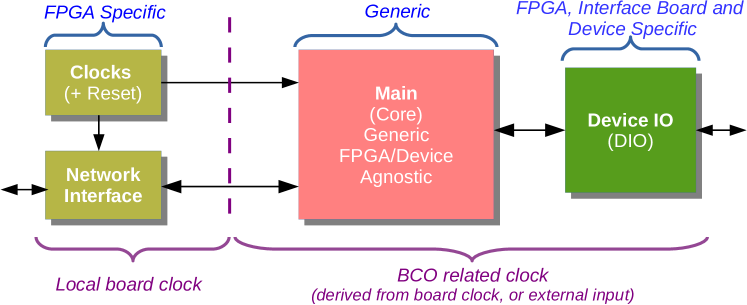
Firmware configuration and control signals are distributed as needed around the FPGA using the “Opcode Bus” (see figure 23). Some of these are responsible for sending serial streams to the DUT. Data returned from the DUT is often multiplexed as a pair of streams sharing onto a single line, implying 2 logical streams per physical link. Each stream is allocated a dedicated “Readout Unit”, which has a packet detector, decoder, histogrammer and FIFO. A large multiplexor funnels all the data received into a single connection to the network interface block.
Note that 640 Mb deserialisers are used in the firmware regardless of data rate. This allows for both simpler coarse delay setting, and non-clock rate dependent decoding of multiple software selectable rates.
3.2.4 Opcode sub-system
Opcodes are the means of communicating directly with the various functional blocks inside the firmware (and the firmware with the software). They allow transfers of blocks of data to firmware “handlers”. All handlers are connected to a common “opcode bus” and pull blocks of data addressed to them. All opcode handlers will send a response when addressed - any data that may have been requested, or just an acknowledge to signal operation complete.
Examples of opcode handlers are: register block (allows writing to a traditional register space), status block (returns a block of status words), two-wire (interface to various slow control protocols) and raw-Signal (send payload contents as a serial stream).
An “opcode” consists of an opcode-ID, a sequence-number and a payload-size field, along with an (optional) data payload - see table 3.
| Field | Size | Description |
|---|---|---|
| OpcodeID | 16 bit | Specifies which opcode-handler is |
| being addressed | ||
| OC-Sequence No. | 16 bit | Generated at source |
| Replies have same as initiating opcode | ||
| Payload Size | 16 bit | Payload-data length in bytes (0 is valid) |
| Payload Data | 0-725x16 bit | Composition format Unique to each |
| opcode-type (opcode-id) |
3.2.5 Software
The software part of ITSDAQ is primarily developed to run on PCs running Linux (for example CentOS 7). A Microsoft Windows version was also been maintained for most of the period in question. It relies on ROOT [29] for histogramming and fitting for analysis and for the graphical user interface.
The software is used to collect data from the ASICs in various conditions, which usually involves scanning over particular settings of the ASIC registers and recording the data response.
A basic test thus involves:
-
1.
Load full configuration to ASICs
-
2.
Set parameter under test
-
3.
Send trigger pattern
-
4.
Record data response
-
5.
Repeat from 3 until number of triggers complete
-
6.
Repeat from 2 until all parameter values scanned
A wide variety of trigger patterns is available so that (for instance) charge can be injected into the front-end with particular timing. A non-exhaustive list includes the addition of different reset commands, sending multiple triggers (and potentially recording data from only one), sending register read commands and sending arbitrary patterns (see section 2.2.1).
Recording the response data normally involves decoding the pattern of hit strips and building a hit map accumulated for all trigger patterns with the same parameter setting. Additional modes include recording the raw bit stream sent by the ASICs, and extracting particular parts of responses (for instance chip ID, or the address or value in a register read).
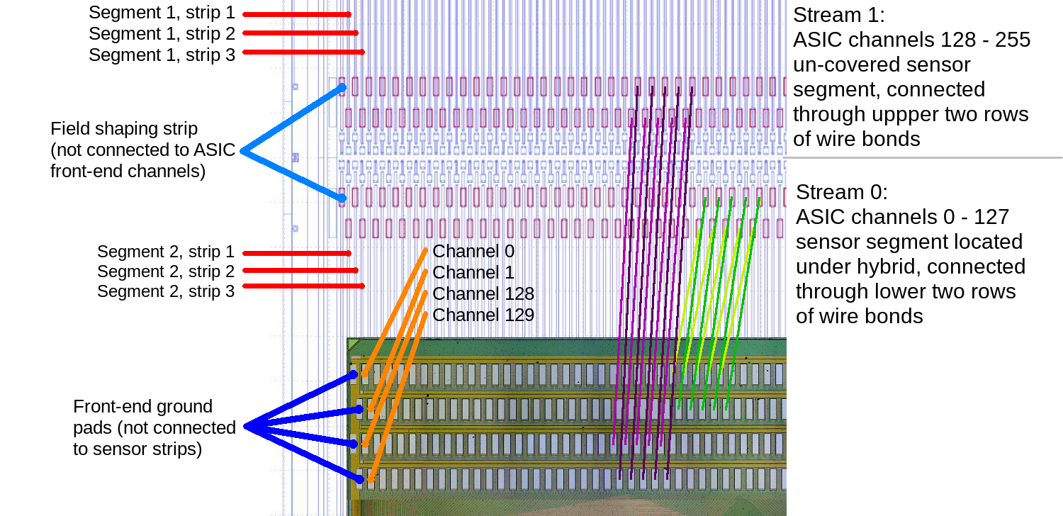
Though the ABC130 ASICs have 256 channels, half of these are bonded to strips running under the ASIC and half are bonded running away from the ASIC (see figure 25). Thus a pair of histograms is produced for occupancy plots for each of these sets of channels. Where plots show 128 channels per ASIC, an arbitrary choice between these sets has been made.
3.2.6 Characterisation Tests
In order to characterise both hybrids and modules electrically, a sequence of tests is performed. This starts with digital tests where the response data is expected to be either all or nothing.
Following this are a series of analogue tests with a variable response. As the hit decision is binary, analogue values are extracted by sending and accumulating data from multiple triggers.
The current set of digital tests are as follows:
-
•
Capture HCC and ABC IDs
This function tests whether communication with all ASICs is possible. If successful, the ID numbers assigned to each ABC130 and HCC130 ASIC are read out. -
•
NMask
This diagnostic test changes the setting of the mask register and uses the send mask feature to produce a deterministic pattern on the output.
The analogue tests mostly involve using the charge self-injection function of the ABC130 (see section 2.2.1). This involves sending a particular command to the ASIC, followed by an L0 trigger. This simulates a strip hit using the discharge of an internal capacitor via a timed pulse. The timing of this pulse (aka strobe) within a clock period can be adjusted by passing through some number of buffers. The pattern of strips into which charge is injected can be changed arbitrarily, which allows different patterns of neighbouring strips to be injected independently. In this case, an additional loop is applied so that charge is injected into all strips when integrated over the full scan. How many strips enabled at each step is configurable, in addition to the number of triggers in each loop.
The current set of analogue tests are as follows:
-
•
Strobe Delay
Before using the calibration injection for other tests an appropriate delay value is chosen. The correct setting varies between ASICs due to process variations and over time due to sensitivity to conditions such as temperature. During a Strobe Delay scan, a charge of approximately 4 fC is injected into each readout channel, which is subsequently read out repeatedly at a readout threshold of approximately 2 fC. The varying parameter is the delay in the injection strobe (between the clock edge and the pulse generation), over the full range of potential delays (6-bits representing approximately 80 ns). The compression mode is set to detect the edge of the pulse, so this finds a window of strobe delay units in which the injected charge is registered in a particular clock (see figure 26). The correct setting, for subsequent tests, is chosen based on the timing of the edges of this window. The delay is set for each individual ASIC at 57 % of the distance from the rising edge. This value was selected based on a more detailed scan of the pulse shape and the noise and gain at different delay values.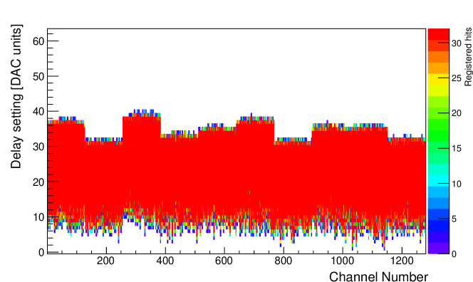
Figure 26: Example of a Strobe Delay scan for a hybrid with ten readout chips. For a range of delay settings, signals are injected to each channel 32 times per setting. Increasing delay means moving from the falling edge (where channels are not aligned) to the rising edge (where channels are more sharply aligned) of the pulse. Each channel registers all injected signals over a range of about 26 DAC units. The delay for each ASIC is set at 57 % of the pulse width from its rising edge. -
•
Three Point Gain
The response of the amplifier for each readout channel is measured using a sequence of threshold scans, where a different charge is injected for each. During the threshold scan, the discriminator threshold is varied. For each injected charge, the resulting distribution is expected to be a step function, which becomes an “S-curve” (a complimentary error function) due to smearing from noise effects (see figure 27(a)). The shape and slope of the S-curve can be used to determine the noise and Vt50 of each input channel (see figure 27(b)). Vt50 describes the mean amplifier response for an injected charge, i.e. the point of the curve where 50 % of readout triggers lead to a hit being registered. By performing threshold scans for different input charges (e.g. 0.5 fC, 1.0 fC and 1.5 fC), the relation between input charge and readout threshold can be mapped and each readout channel’s gain be determined using a linear fit (see figure 27(c)). Additionally, the offset of the gain function of each channel is determined. Figure 27(d) shows the resulting noise distribution for one hybrid with ASICs. This gain can be used to convert the output noise (the measured width of the S-curve) into the input-referred noise (the derived noise at the input of the amplifier), which is then reported in electrons (of equivalent noise charge).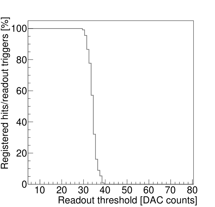
(a) S-curve obtained from a threshold scan of a readout channel. 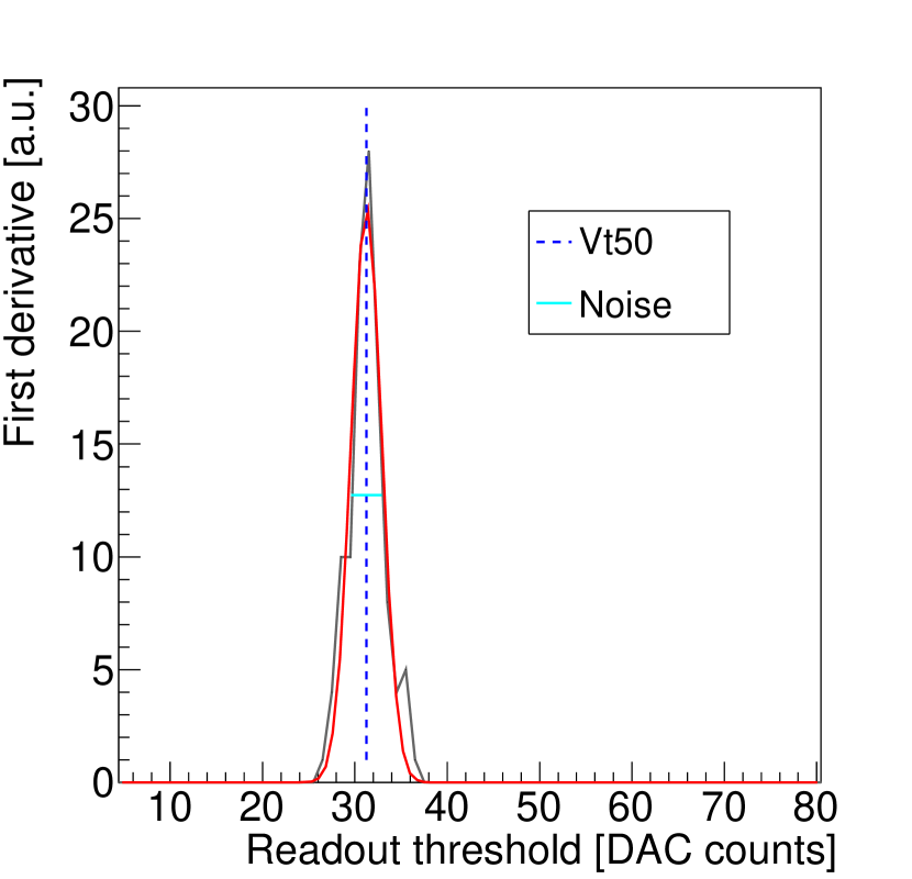
(b) First derivative of an S-curve with Vt50 and noise. 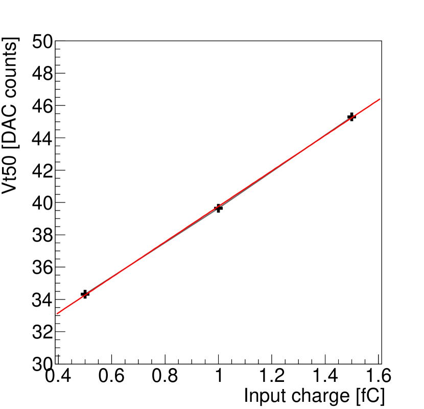
(c) Gain of individual readout channel, from Vt50 measurements. 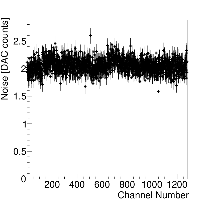
(d) Noise of channels from all ASICS on one hybrid (about 400 ENC). Figure 27: Examples from a Three Point Gain measurement of one hybrid: measurement of the S-curve of an individual channel, mean of noise and Vt50 for that channel, gain calculation from measurements at different input charges and noise distribution for one hybrid. It should be noted that while threshold tests and their analysis are performed based on ASIC DAC counts (referring to bit register settings), the corresponding threshold (measured in mV) does not increase linearly with DAC counts over the full range of thresholds (see figure 31) and is only converted into mV during the last step of the analysis.
-
•
High statistics Three Point Gain
While the standard Three Point Gain performed on hybrids (see section 3.3) is sufficient to identify dead channels, the uncertainties of parameters derived from a fit of the obtained S-curve (see figure 27(a)) depend on its statistics. Increasing the number of triggers used for the measurement of an S-curve leads to more reliable channel characteristics (see figure 28).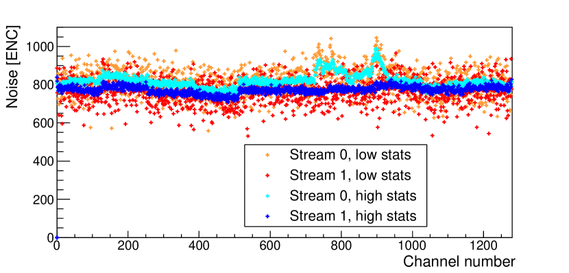
Figure 28: Comparison of channel noise measured for one hybrid on a barrel module from Three Point Gains with high (1000 triggers per threshold) and low (50 triggers per threshold) statistics. Noise fluctuations were found to be reduced by the number of applied triggers, which shows increased noise in certain module regions (caused by insufficient powerboard shielding, see section 4.7) that are hidden in overall noise fluctuations for a measurement with low statistics. Due to the time consumption of full threshold scans with high statistics, modules were tested with low statistics thresholds scans first to check their overall functionality before performing an additional high statistics Three Point Gain.
-
•
Trim Range
During the operation of a module, readout thresholds are not set for individual channels, but for full readout chips. An operating threshold is chosen to be as low as possible while also minimising noise occupancy (). S-curves from different channels from the same module show a large spread over the threshold range (see figure 29), which makes the selection of an operating threshold less efficient, as a threshold with less than 1 % noise occupancy for all channels leads to a wide range of distances between operating threshold and Vt50 point.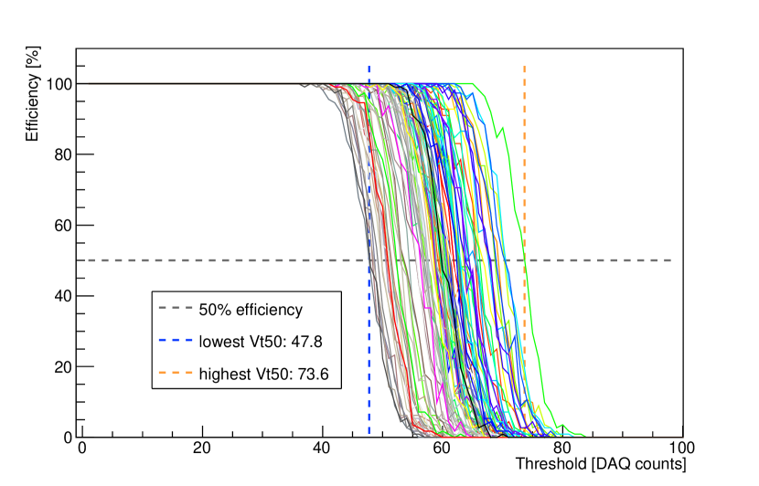
Figure 29: S-curves for 100 sequential channels on an ABC130 module without trimming: the positions of their Vt50 points are distributed over a range of 26 DAC counts. In order to ensure a uniform response of all module channels to which the same readout threshold is applied, S-curve positions can be shifted in the threshold range. While an efficiency curve can not be moved towards lower thresholds, it can be moved towards higher thresholds by adding an offset, which has to be determined by channel, to the pedestal. In order to find a threshold to which a majority of channels can be trimmed, a scan over the TrimDAC values and the Trim Range is performed. A chosen charge is injected into the front-ends and the trims adjusted so that the thresholds align for a particular chip-level threshold. The Trim Range (the scale of the trim changes) is chosen to be allow as fine tuning as possible while including as many channels as possible. Thus, all channels on a chip are trimmed by adding the tuned offset value to their threshold, leading to a uniform distribution of Vt50 on all channels of the same chip (see figure 30).
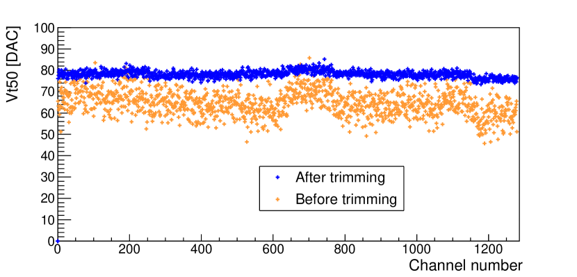
Figure 30: 50 %-efficiency point (Vt50) of channel S-curves before and after performing a Trim Range: before trimming, Vt50s of channels show a large spread. After trimming, channels on the same readout chip show a flat distribution of Vt50 at a higher value, which is achieved by adding to the pedestal of S-curves with low Vt50. -
•
Noise Occupancy
The noise occupancy test records channel occupancy with no injected charge. This is carried out for a series of thresholds in order to extract the noise curve of the pedestal. A variety of options are provided for the timing and number of these triggers. -
•
Response Curve
In the response curve test, the correspondence between input charge and threshold is further characterised, beyond the linear regime of the Three Point Gain test (see figure 32), for higher input charges and corresponding thresholds and where the relationship becomes non-linear. This uses ten threshold scans over a range of input charges up to 6 fC. The correspondence between DAC count and threshold voltage is approximately linear over a large range of these settings, an option is provided to make a correction base on based on a simulation of the relationship (see figure 31), for greater accuracy.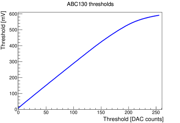
Figure 31: Calibrated relation between ABC130 threshold setting and corresponding physical threshold: the corresponding threshold increase is linear for low thresholds, but becomes non-linear for high thresholds. 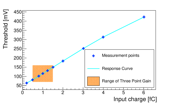
Figure 32: Response Curve for an average of all readout channels on an ABC130 readout chip: the relation between input charge and readout threshold is linear for low threshold and becomes non-linear for high thresholds. The input charge range covered in a Three Point Gain scan (performed at 1 fC) is highlighted in orange. Performing a Response Curve allows to relate the ABC130 threshold setting, physical readout threshold and input charge.
3.3 Hybrid tests
Flexes with ABC130 ASICs and an HCC130 chip can be tested for electrical functionality, which is used to identify nonfunctional hybrids prior to the assembly of hybrids, powerboards and sensor into a module. In order to test assembled hybrids, hybrids are electrically connected to a hybrid panel, which serves as a test structure using wire bonds to supply power and read out data.
Each panel provides test positions for eight hybrids, which can be tested in parallel, provided that the HCC130 on each hybrid has been assigned an HCC130 ID different from HCC130 IDs of the other seven hybrids.
A test sequence for hybrids includes the following steps (described in detail in section 3.2):
-
1.
Capture HCC and ABC IDs
-
2.
Strobe Delay
-
3.
Three Point Gain
A hybrid is only mounted on a sensor if it has passed all stages of electrical testing.
3.4 Powerboard assembly
The powerboard v2 is produced in a thin FR4 based stack-up and loaded with SMDs in a typical reflow process. The DCDC inductor due to its shape is loaded manually, as is the shield box enclosing the DCDC circuit. Special attention is given to fully seal the shield box with a continuous solder seam to avoid leakage of radiated noise. Once proper SMD loading has been verified in a visual inspection, the bare die ASICs, the AMAC and HVmux, can be glued to the powerboard v2 and wire bonded.
For testing the powerboard is temporarily wire bonded to a test carrier PCB, which can be seen in fig. 33. This carrier can now be connected to test equipment to test the functionality of the powerboard before loading it onto a module. The test carrier also provides passive cooling, which is necessary to run the DCDC circuit at high load current without overheating the FEAST chip.
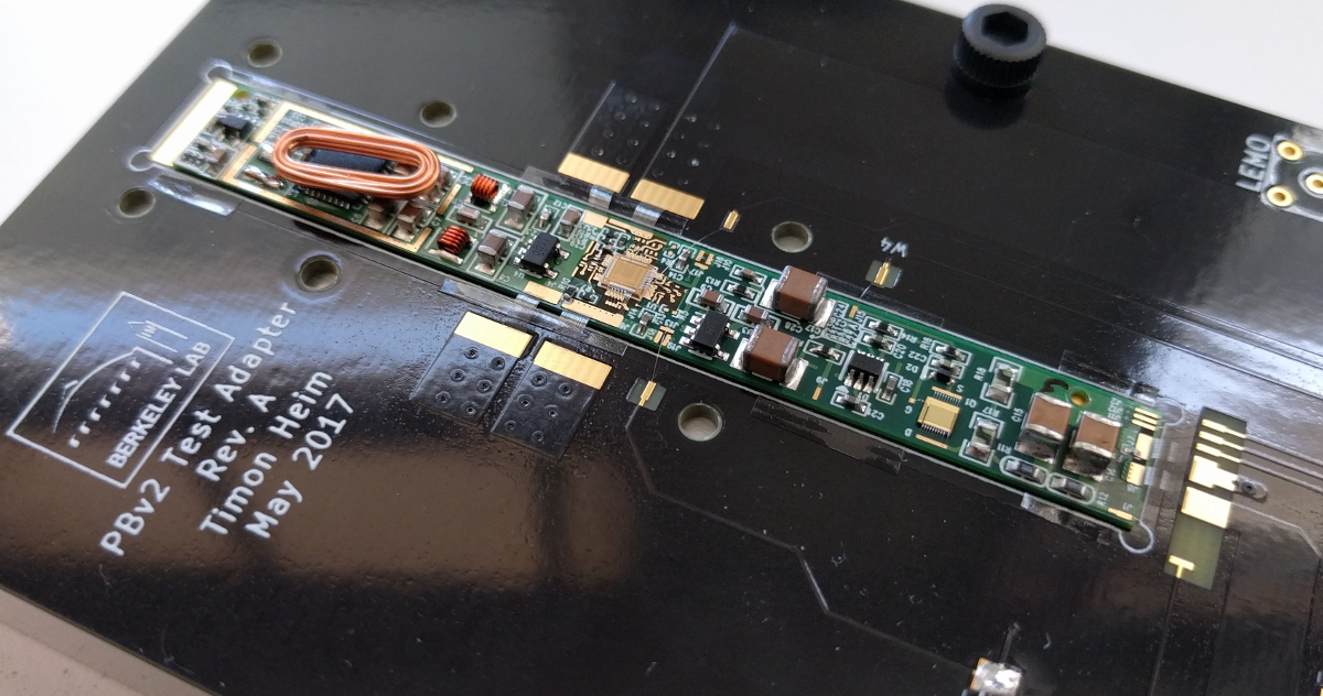
3.5 Powerboard tests
To test the functionality of the powerboard before loading it onto the module and to calibrate the AMAC the following tests are performed:
-
•
AMAC communication test: ensures reliable communication with the AMAC
-
•
LV turn on/off: ensures functionality of switching 1.5 V of DCDC to hybrid on/off
-
•
HV turn on/off: ensures functionality of switching HVmux to supply high voltage to a sensor
-
•
DCDC efficiency: measures DCDC efficiency for load currents from 0 to 4 A
-
•
calibration: varies input voltage, which is measured by the AMAC
-
•
calibration: varies output load, which is measured by the AMAC via an amplifier measuring the voltage drop over the inductor in the output -filter
-
•
HV sense calibration: varies the current sources by the HV power supply, which is measured by a current-to-voltage converter in the AMAC
-
•
Temperature calibration: vary the output load to change the temperature of the powerboard and measure this via the thermistor inside the shield volume and temperature sensor within the FEAST chip
All of the test results are saved and a calibration is derived for each monitored value. During testing of 100 powerboard v2 boards only hard failures have been observed, typically caused by errors during SMD reflow or dead ASICs, as chips were not tested before loading.
3.6 Sensor tests
Sensors are electrically tested upon reception from the vendor, and additional tests are carried out after shipment to module assembly sites. Reverse bias leakage current (IV) characteristics are determined by raising the bias voltage in 10 V steps, observing a 10 s delay before reading the current. An example IV curve is plotted in figure 34(a): the leakage current is well behaved up to -1000 V.
Reverse bias capacitance curves are measured by an LCR meter using a frequency between 1 and 5 kHz and 100 mV amplitude. The full depletion voltage () is extracted from the intersection of two straight line fits to the curve of versus voltage: one line is fitted to the linear slope below the , the other is fitted to the flat section above . The depletion voltage is indicated by the red arrow shown in figure 34(b).
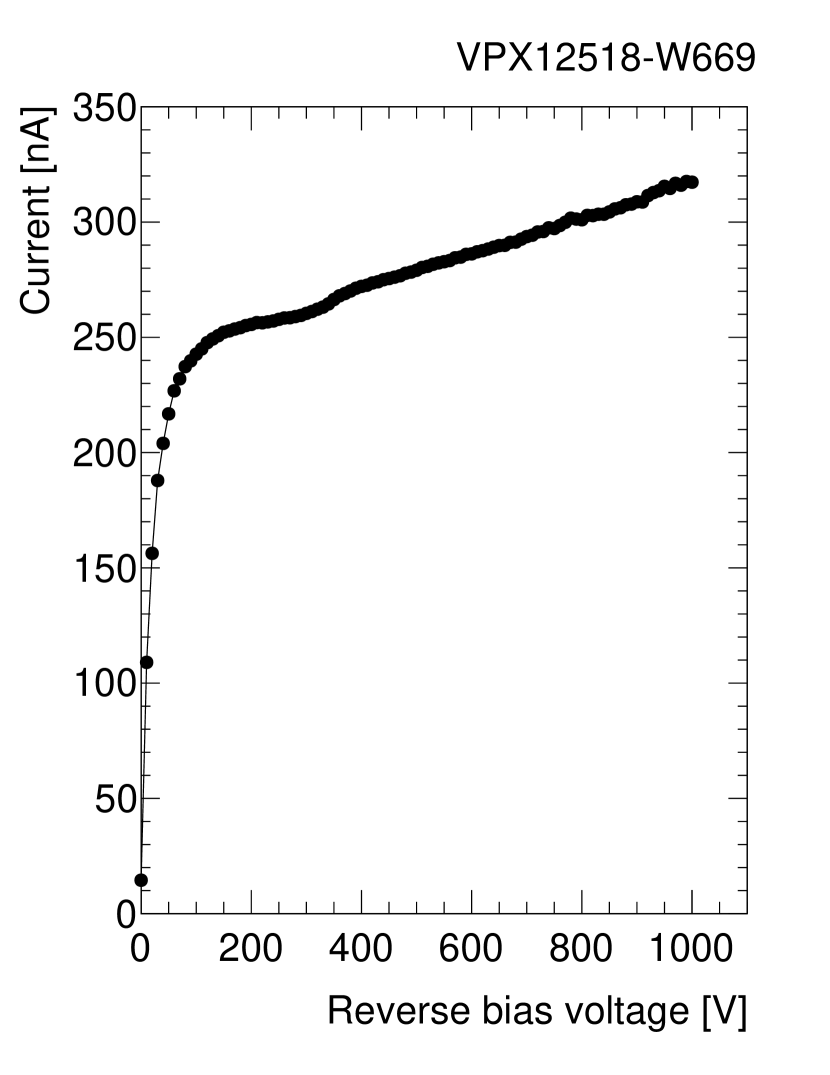
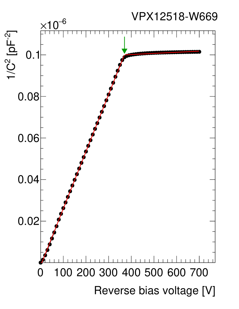
The depletion voltage was extracted for all sensors and found to be -370 V on average for the investigated sensors. An overview for a subset of 68 ATLAS12 sensors is shown in figure 35.
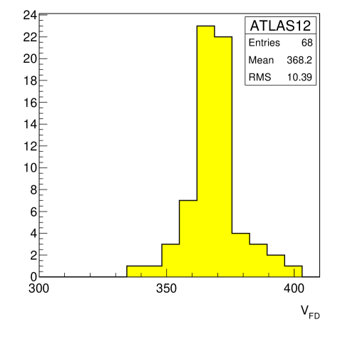
Full strip test measurements were carried out on the barrel sensors, whereby successively -10 V, -100 V is applied across the strip metal and bias rail to check for short circuits or oxide pinholes, respectively. An LCR meter (1 kHz, 100 mV) is used to determine the R and C values of the AC circuit formed by the bias resistor and capacitance between the strip implant and strip metal.
The specification for the sensor bias resistance is 1.50.5 M and the strip AC coupling capacitance is required to be 20 pF/cm. The measurements discussed above were compared against these values, and the number of channels outside these specification was found to be on average 5 out of 1280 channels (with the specification requiring a minimum of 98 % good channels). Figure 36 shows an overview of the number of bad channels per sensor found on 100 sensors.
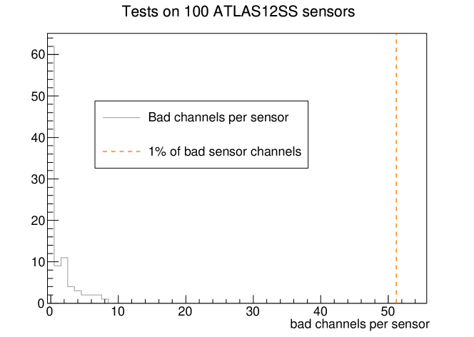
In addition, the maximum number of pinholes was required to be at most seven per 1280 sensor strips, which were required to not form a cluster of eight or more for an individual sensor segment.
3.7 Module assembly
Successfully tested hybrids, powerboards and sensors were assembled into modules in a gluing process similar to the assembly of hybrids: First, sensors are aligned on a precision vacuum jig using three alignment pins (see figure 37). After positioning the sensor, vacuum is applied to the sensor backside to hold the sensor in position and keep it flat during the assembly process.
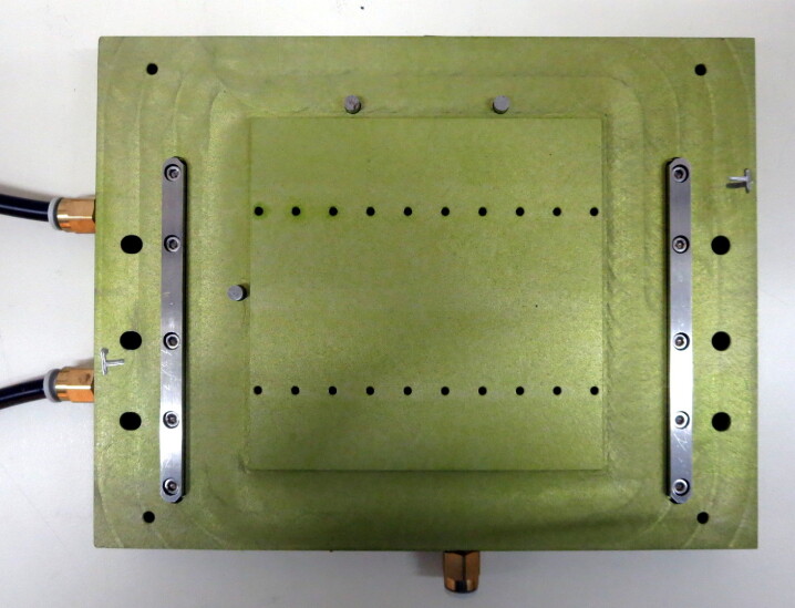
Hybrids had to be mounted on the sensor surface before the powerboard, as the powerboard shield box on the powerboard prevents the positioning of the hybrid pick-up tool at the correct height. At this stage, hybrids were still located on individual positions on hybrid panels, where they were populated with ASICs and tested. Prior to assembly into modules, the wire bonds connecting hybrids to the power and data lines of a panel need to be removed.
Hybrids are then lifted from the hybrid panel using a hybrid pick-up tool (see figure 18), which is located using the hybrid panel alignment holes (see figure 16) and thereby ensures the correct hybrid position with respect to the pick-up tool alignment pins.
A two-component epoxy (Epolite FH-5313) was used to attach hybrids and powerboards to sensors. Over the course of the barrel module programme, an extensive study was conducted to investigate potential epoxy glues for module assembly [24], which yielded two additional candidates: Eccobond F-112 and Polaris PL-5313. Polaris PL-5313, the successor of Epolite FH-5313, was chosen as the baseline for module assembly during production and Eccobond F-112 as the alternative.
During the ABC130 barrel module programme, eight modules were assembled with F-112 and PL-5313 adhesives each, while the majority of modules was constructed using Epolite FH-5313. Since no difference was observed for modules assembled with these three adhesives, they will not be distinguished further in the text.
The mixed adhesive was applied to the hybrid backside using a glue stencil mounted on the hybrid pick-up tool (see figure 38). In order to ensure a sufficient glue viscosity for the use of a stencil, a waiting time of up to 20 min was used between mixing both epoxy components and applying the glue.
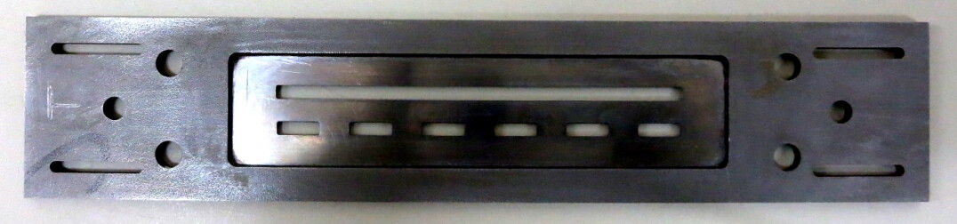
After dispensing the adhesive, the stencil was removed and the hybrid positioned on the sensor and held in place using a brass weight. A stencil thickness of 250 m was chosen to produce corresponding glue layers. By positioning the hybrid pick-up tool on dedicated landing pads in the module assembly jig, the glue layer between hybrids and sensor was compressed to a thickness that was set using adjustment screws on the pick-up tool. The target glue thickness between hybrid and sensor was chosen to be m, which corresponded to a 50 % thickness compression (assuming a 100 % stencil fill factor) and therefore a doubling of the glue area for good mechanical support below the hybrid. A minimum curing time of 6 hours was used before turning off the vacuum holding hybrid and sensor at a defined distance. Since glue spreading over the sensor bias ring was found to cause early sensor breakdowns in several cases [24], the sensor current was monitored after individual gluing steps.
ABC130 barrel modules can be tested (see section 3.8) without a powerboard attached to the module. An additional module test was therefore performed between hybrid and powerboard attachment, so that the impact of mounting a powerboard on a module could be studied directly (see section 4.7). In order to test the module performance, each ABC130 readout channel was connected to a silicon sensor strip using aluminium wire wedge bonding. Front-end bonds (i.e. wire bonds connecting the analogue ABC130 readout channels to the sensor) were drawn in four rows arranged in layers (see figure 39). Out of the four rows of staggered sensor bond pads, the lower two rows (64 wires each) were attached to the inner strip segment of an SS module (or the sensor segment located beneath hybrid and powerboard of LS modules), the upper two rows were connected to the outer segment of an SS sensor (or sensor segment without hybrid and powerboard on an LS module), see figures 3(b) and 3(a).
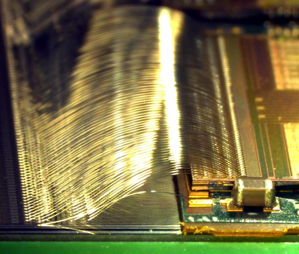
Different from hybrids, the layout of powerboards did not allow them to be picked up using vacuum pick-up tools, as the high density of components mounted on the powerboard did not leave enough space for reliable vacuum connections. Powerboards were therefore held along the PCB edges using a width adjustable tool that could be tightened around the powerboard edges using screws (see figure 40).
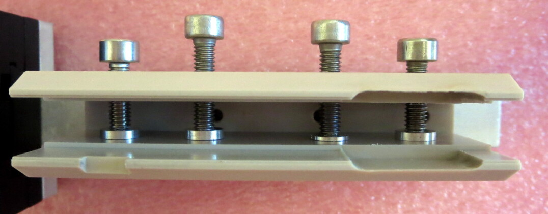
After picking up the powerboard and fixing it in position, glue was applied to the powerboard’s backside (see figure 41(a)). Powerboards were attached to sensors using the same two-component epoxy used between hybrids and sensors: Epolite FH-5313. Afterwards, the powerboard was placed between two hybrids on an SS module (see figure 41(b)) or next to one hybrid on an LS module, with a gap of about 1 mm between hybrid and powerboard edge to facilitate wire bonding.
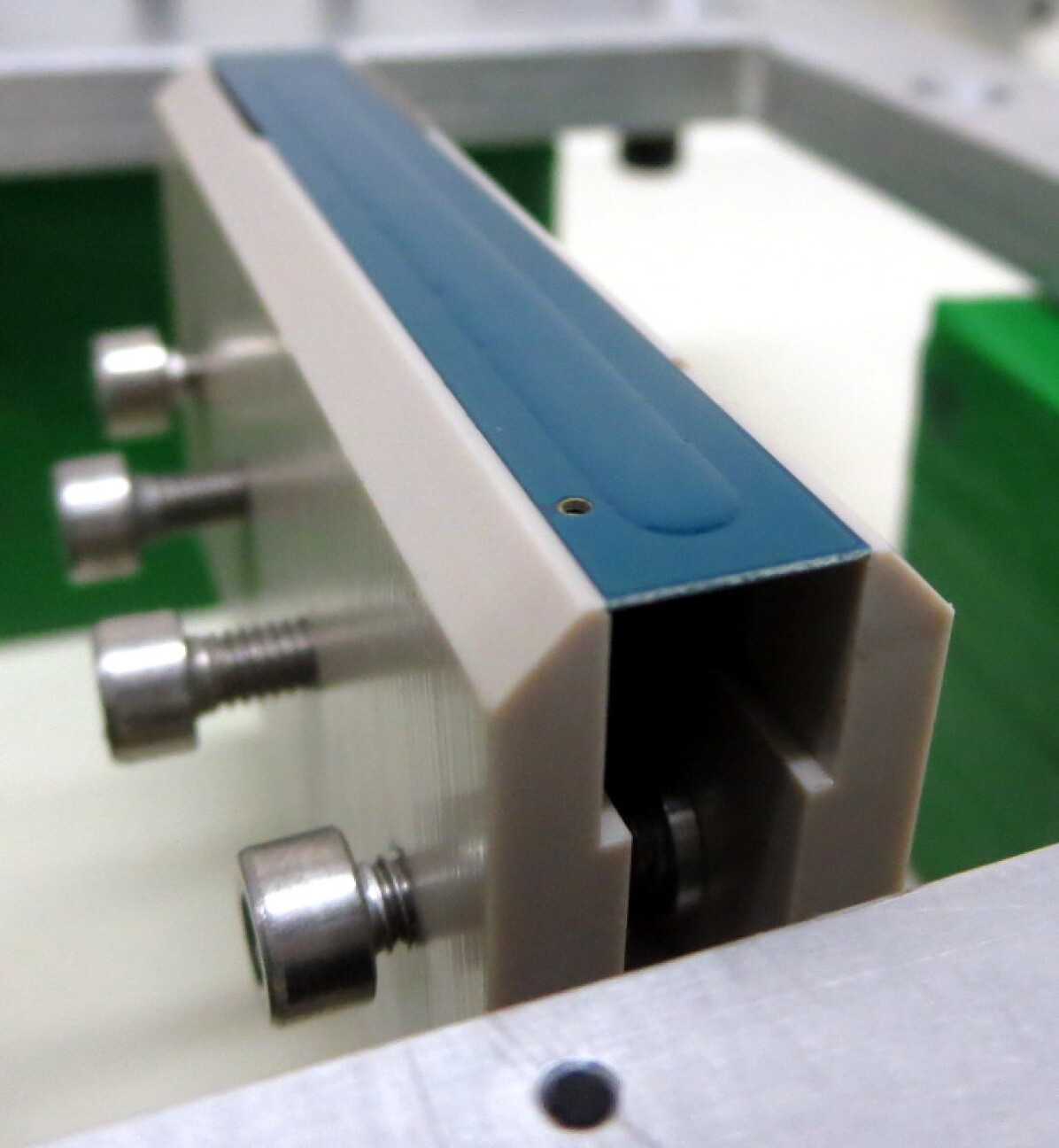
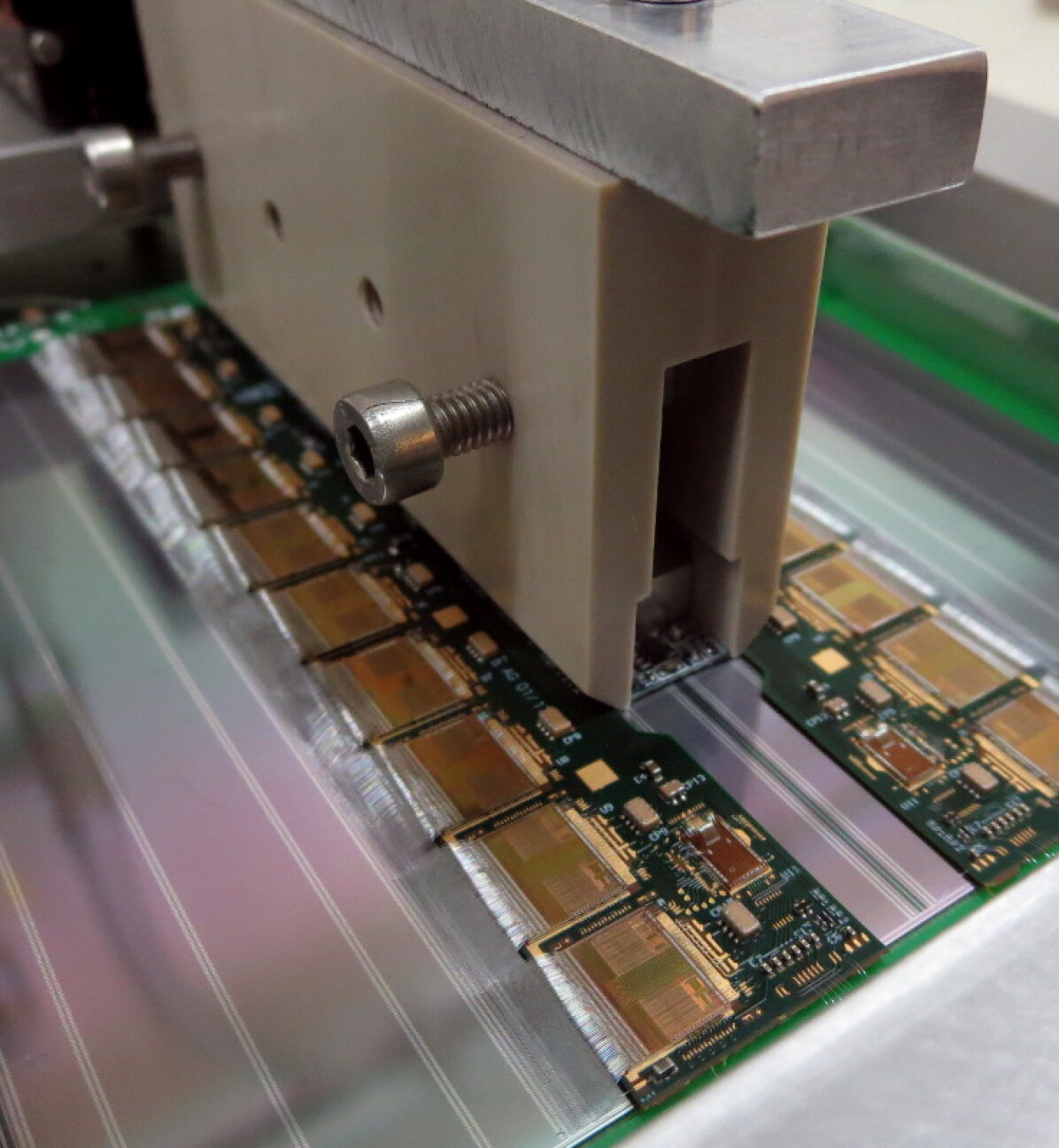
Similar to the tools used to mount hybrids on sensors, powerboard gluing tools can be adjusted to set the target glue height of m prior to assembly (see figure 42).
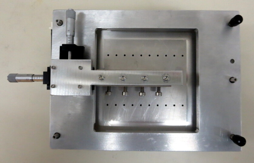
After positioning a powerboard on a module, vacuum pressure was maintained throughout a curing time of at least six hours.
Since powerboard assembly tools were still under development during the ABC130 barrel module programme, part of the modules were assembled without the tools being available. In these instances, modules were assembled by placing powerboards on the module by hand.
During the ABC130 barrel module programme, the method of holding a powerboard along its edges for assembly was found to lead to uneven glue thicknesses in case of warped powerboards or irregularities along the powerboard edges. Subsequent versions of powerboard pick-up tool were therefore designed to use vacuum pickup pins (similar to hybrid pick-up tools). Additionally, the powerboard design for the next generation of readout ASICs was modified to increase the size of areas suitable for vacuum pick-up.
3.7.1 Sensor metrology after module assembly
For the attachment of modules onto support structures, modules are required to have a bow of no more than , where positive numbers refer to the module centre being below the edges. While sensors themselves typically conform with this envelope upon delivery, the assembly process of modules, during which sensors and PCBs are held flat using vacuum tools, can affect the overall sensor bow. In order to monitor the impact of gluing on the sensor shape, dedicated metrology measurements were performed at different stages of module assembly (see figures 43(a) to 43(d)): using a white light interferometer system, the absolute sensor height was measured for a fine grid of inspection points (see figure 43(a)). The sensor shape was mapped based on the measured heights and the sensor bow was calculated based on a fit through the sensor plane.
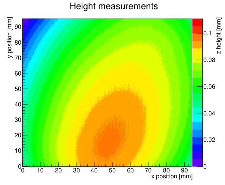
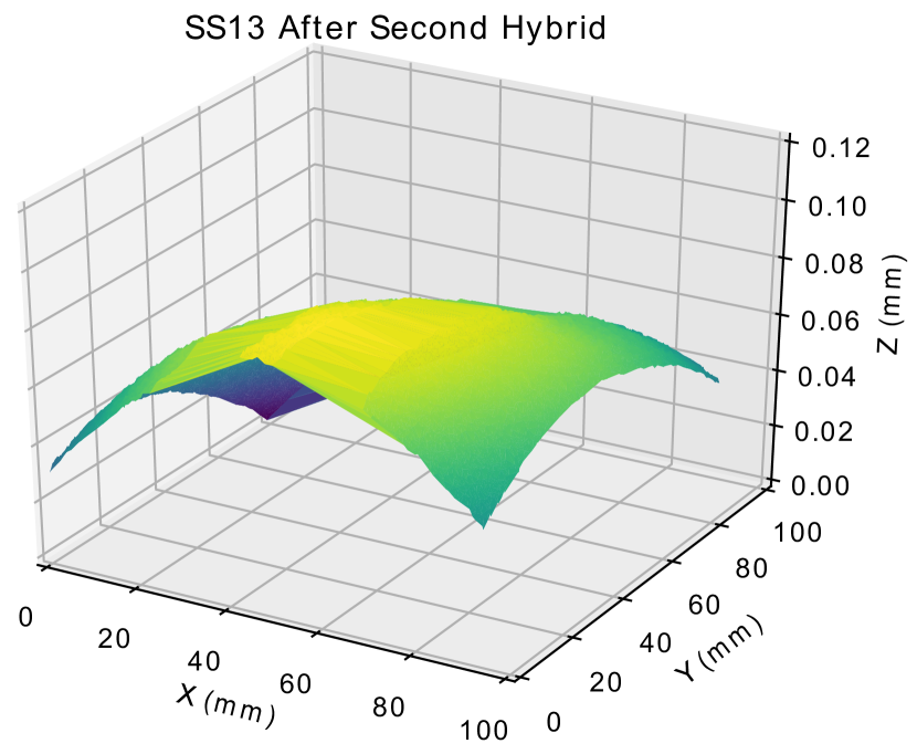
After each measurement, the overall sensor shape and maximum height deviations were calculated. Examples for four modules are shown in table 4.
| Maximum difference, | |||
| Module | Sensor | First hybrid | Second hybrid |
| SS12 | 76 | 83 | 103 |
| SS13 | 103 | 101 | 93 |
| SS14 | 84 | 85 | 95 |
| SS15 | 96 | 119 | 98 |
Measurements did confirm that the attachment of hybrids to a sensor affected the sensor shape and changed the distance between the maximum and minimum deviation from the sensor plane by up to 27 m. All modules were found to be within the specifications at all stages of assembly.
3.8 Module tests
For electrical tests, modules are connected to dedicated test frames (see figure 44), through which power is supplied and data is read out.
In order to apply high voltage to the sensor backside, test frames have a cutout that allows a direct contact between the sensor backside and a testing jig. During testing, vacuum holes hold the sensor on the high voltage testing jig. Additionally, a cooling loop embedded in the testing jig is used to maintain a constant sensor temperature during testing. Condensation on the cooled module is prevented by flushing the test setup with dry air or nitrogen.
The powering concept of ABC130 modules allows the testing of directly powered hybrids as well as hybrids powered through a powerboard (see figure 45).
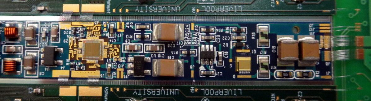
Since the attachment of hybrids and a powerboard are separate steps in the construction of modules, which can lead to sensor damage, causing e.g. an early sensor breakdown, modules were tested both after hybrid attachment and after powerboard attachment, permitting a comparison of the module performance at both stages (see section 4.7).
For the full electrical test of a module, the tests performed on electrical hybrids (Capture HCC and ABC IDs, Strobe Delay and Three Point Gain - see section 3.2) are repeated with a fully depleted sensor. Results from the Three Point Gain are used to grade each individual module channel (see table 5) and determine the number of good channels on a module.
| Gain | Noise | |
|---|---|---|
| High | high gain | high noise |
| average chip gain | average chip noise | |
| Low | low gain | dead |
| average chip gain | 0 ENC |
In addition to the test sequence above, more tests can be performed for a full module characterisation:
-
•
High statistics Three Point Gain
-
•
Trim Range
-
•
Noise Occupancy
-
•
Response Curve
These tests provide a complete characterisation of a module such that its quality can be graded.
4 Selected module test results
The aim of the ABC130 barrel module programme was to allow tests of the proposed procedures for assembly, readout and cooling concepts of both modules and integrated structures. Due to the extent of the programme, it was possible to gather statistics on assembly yields and test results and to validate component designs for subsequent component generations.
This section summarises some of the module test results obtained in electrical tests of modules as well as individual components.
In addition to the investigations of individual electrical characteristics presented in the following, performance evaluations of full electrical modules were conducted in particle beams at the DESY-II and CERN SPS facilities [30].
4.1 Dependence on number of strobed channels and triggers
During an internal charge injection test (either three point gain or response curve), two important parameters can be changed in order to optimise the accuracy of the extracted results and the time that the measurement takes. These are the number of triggers (readout requests after charge injections) per threshold value and the number of channels in the ABC130 chip strobed simultaneously.
Figure 46 shows the noise extracted at 1.5 fC from a response curve test as a function of the number of triggers included in the scans. As can be seen, the noise is underestimated when a small number of triggers is used but plateaus as the number is increased. This is because with a small number of triggers the low occupancy tail in the S-curve is underpopulated, which results in S-curve fits returning a narrower noise profile. As the number of triggers is increased, the tail is better populated, resulting in increased, and more correct, noise measurements. This effect has been verified using Monte Carlo simulation.
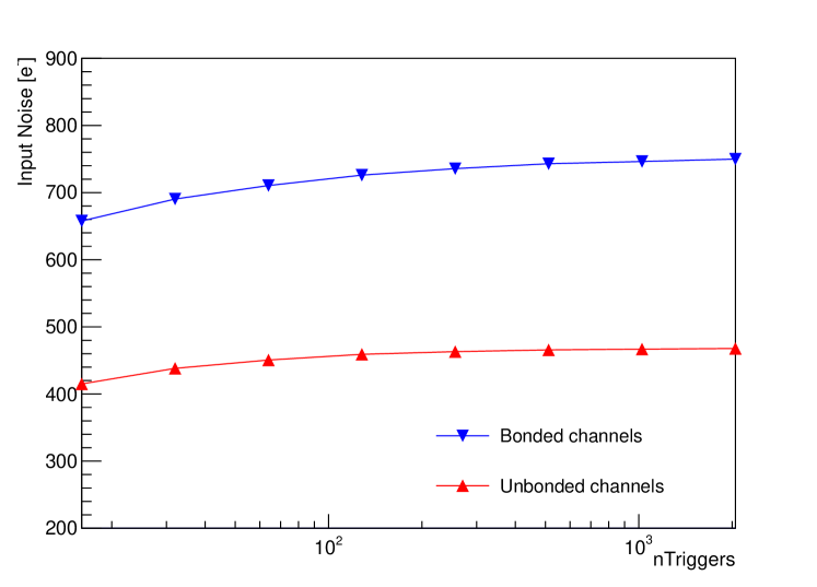
Figure 47 shows the input noise, gain and output noise extracted at 1.5 fC from a response curve test as a function of the number of channels strobed (charge injected) at once compared to that extracted when all 256 channels are strobed simultaneously. The extracted input noise can be seen to reduce as the number of strobe channels decreases. In the response curve analysis, the input noise is calculated as the ratio of the measured output noise (in mV) and gain (in mV/fC) extracted from the response curve. As such, it is useful to look also at the output noise and gain in addition to the input noise. It is seen that the measured gain increases with reducing number of strobed channels whilst the output noise remains constant.
This measurement shows that the charge injection circuitry within the chip does not manage to inject as much charge as expected when strobing many channels at once. This results in a decreased measured gain. In turn, this decreased gain results in increased calculated input noise and thereby explains the decreased noise observed with reduced number of strobed channels. It can also be seen that increasing the capacitive load on the channels by increasing the strip length increases the size of the observed effect.
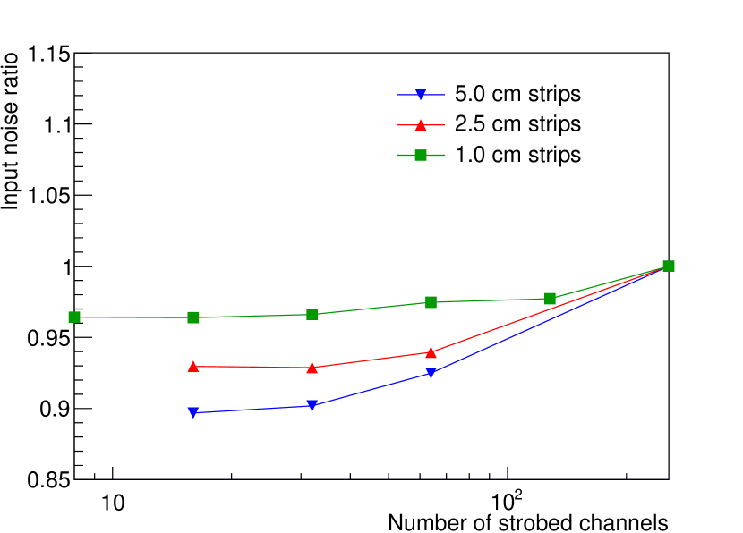
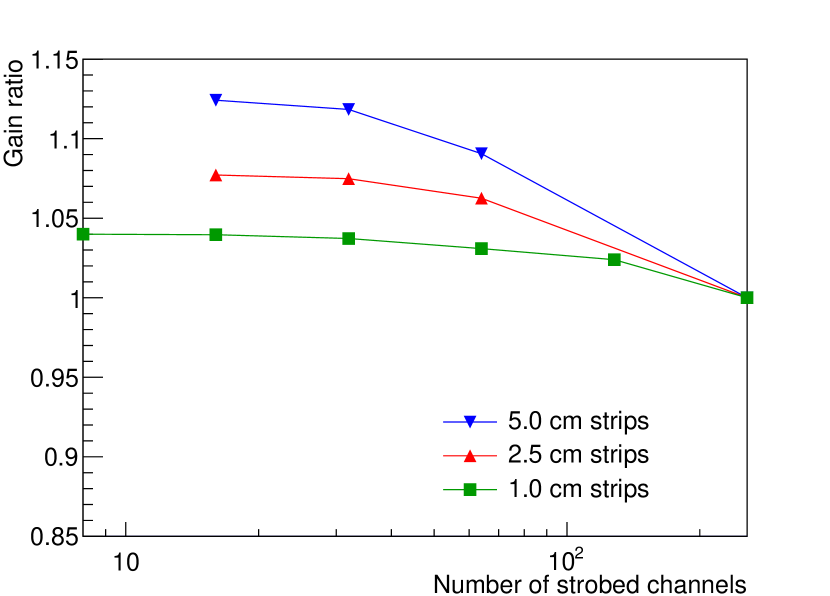
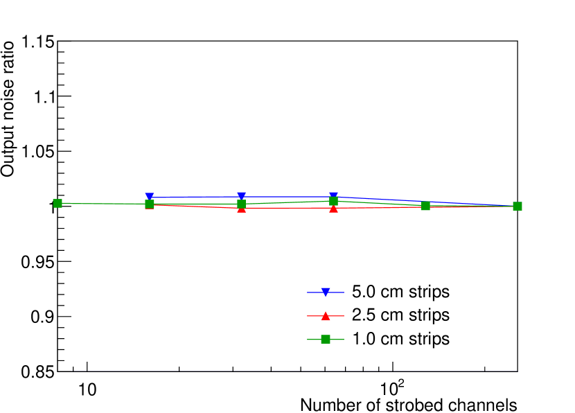
As shown above, the extracted noise depends on both the number of triggers per scan and the number of channels probed simultaneously. During module testing a choice must therefore be made between speed of test, preferring low numbers of triggers and high numbers of strobed channels, and accuracy of the extracted input noise and gain, preferring high numbers of triggers and low number of strobed channels. As a result the decision was made that for quality control module testing, 192 triggers and 256 strobed channels would be the default whilst for the detailed module or chip characterisation tests shown below, 1024 triggers and 16 strobed channels is preferred to ensure that measurements are taken in the plateau of both distributions. Unless otherwise stated, all results below are done with the high number of triggers and low number of strobed channels required to get an accurate measure of input noise and gain.
4.2 Module noise and strip capacitance
The ABC130’s amplifier input capacitance is the leading cause for an increased module noise (before irradiation) compared to the hybrid noise value. Therefore, the ABC130 chip set and modules have been fully characterised by measuring noise and gain as a function of load capacitance using the internal charge injection circuitry. This has been done on 32 channel prototype chips [17], on single chip test boards with either capacitor or mini sensor loads and on short strip and long strip barrel modules. In the case of the prototype, the front end was initially designed for positive signals rather than the negative signals coming from n-on-p sensors and so, results for both positive and negative signals are shown. In addition, results from an irradiated module are included which will be discussed further in Section 4.8. All non-prototype measurements shown are results are taken using the standard measurement configuration described in section 4.1.
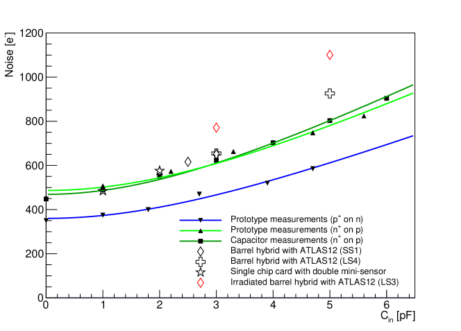
Figure 48 shows a summary of the noise measurements made as part of the ASIC characterisation. Capacitance values for tests performed including sensors are taken as the sum of the inter-strip capacitance and strip-backplane capacitance as measured during sensor probing. In addition, an extra 0.5 pF is included for those strips running under the hybrid, taken from calculation of the expected capacitance increase due to the ground plane running above the strips. Good agreement is seen between prototype measurements and capacitive load measurements performed on full chips. An increase in noise is seen between the capacitor measurements and the short strip and long strip modules. A small increase, at the level of a few percent, is expected for such factors as the bias resistance, metal strip resistance and inclusion of next-to-nearest neighbour inter-strip capacitance. The leakage current contribution is negligible before irradiation, but it increases the noise by 5-10 % at full fluence. Finally, a significant increase in noise is seen during irradiation, which is corroborated by single chip measurements and is a TID dependent effect, which has led to a redesign of the front-end for the next ASIC generation.
Figure 49 shows the noise and gain of an early barrel module. This module was built as a long strip module but using a short strip ATLAS12 sensor. Short strips were then ganged together in such a way so that all channels running under the hybrid (stream 0) are long strips. In addition, strips running away from the hybrid (stream 1) and connected to the two chips at either end of the hybrid were ganged as long strips with the remaining six chips of channels running away left as short strips. This mixed strip module allows simultaneous characterisation of short and long strip channels at once. Results in this plot were taken at 1.5 fC injection charge during a response curve test of 192 triggers and strobing all channels at once.
Firstly, the increased noise associates to channels connected to long strips can immediately be observed comparing the two streams on the six central chips. In addition, the extra 30-50 ENC due to the presence of the hybrid above strips can be seen looking at the two chips at either end, which have long strips connected to both streams but show a slightly increased noise on those channels running under the hybrid. Finally, the gain results demonstrate that the measured gain is independent of the connected load.
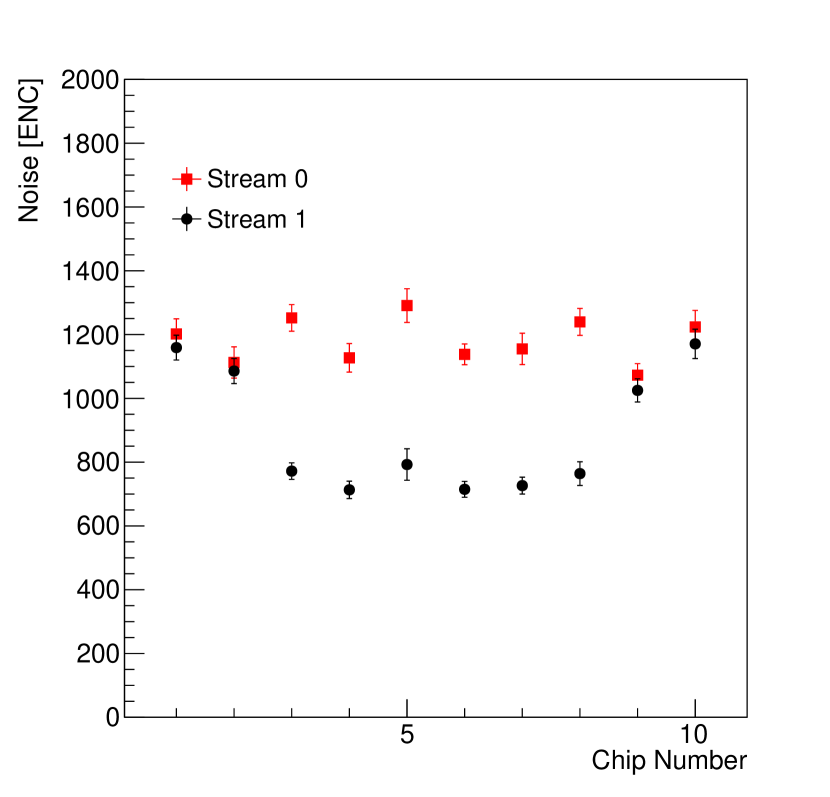
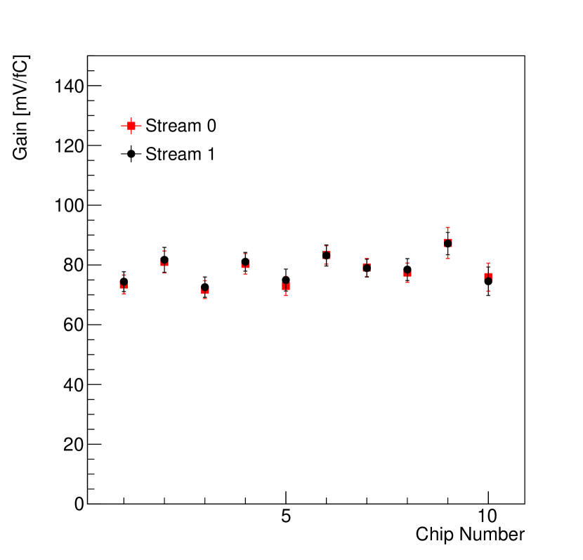
4.3 Noise occupancy results
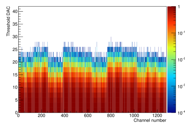
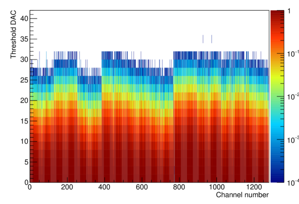
Noise occupancy scans were run on a module in test beam with mixed strip lengths. Strips running under the hybrid were short strips whilst strips running away from the hybrid were ganged together as long strips. Noise occupancy scans without external charge injection are shown in figures 50(a) and 50(b). These results were taken with the module trimmed to 1fC injected charge. Results are shown as a function of the 8-bit register setting of the threshold.
Chip-by-chip averages across 128 channels per chip are shown in figure 51. Threshold settings in DAC have been converted to mV using calibrations from simulation whilst conversion from threshold voltage to charge have been taken from the chip-by-chip response curve results obtained using the internal charge injection circuitry using 1024 triggers and strobing 16 channels at a time. The chip-by-chip results are then fitted with the complementary error function, the width of which can be used to extract the input noise of the system.
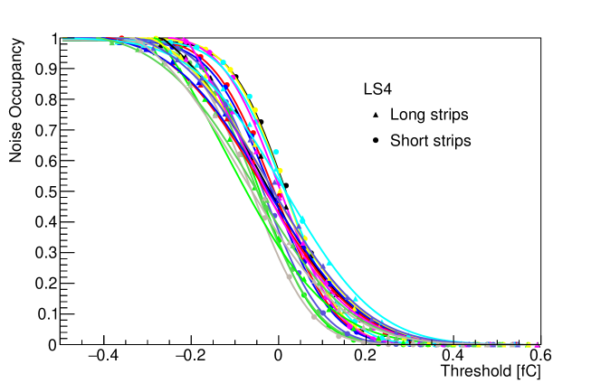
Assuming that the shape of the noise occupancy is Gaussian, the tail of the noise occupancy can also be used to extract noise from this data by plotting the natural logarithm of the noise occupancy versus the square of the threshold. The result of this is shown in figure 52. As expected, the chip-by-chip averages clearly separate into two populations dependent on long-strip or short-strip. It can also be seen to a very good approximation that the tails of the noise occupancy are indeed Gaussian as demonstrated by the linear trends shown down to very low noise occupancy. In addition, the gradient of linear fits to this data can be used to extract the measured noise of the system.
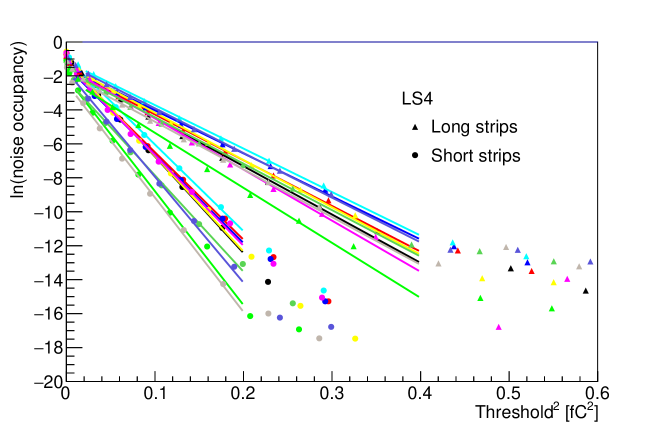
4.4 Comparison between Noise Occupancy and Three Point Gain
Three methods by which noise can be extracted from module testing results have been shown above:
-
•
that extracted from internal charge injection measurements (extracted at 1.5 fC from a response curve)
-
•
that extracted from a complementary error function fit of the noise occupancy data
-
•
that extracted from a linear fit to the natural logarithm of occupancy versus the square of threshold
The latter two, although based on the same data are driven by different parts of the distributions as the complementary error function extraction is dominated by the core of the noise occupancy S-curve whilst the linear fit is driven by the shape of the tail of the S-curves.
Figure 53 shows a comparison of the noise extracted from the three methods. For the short strips on the module, all three methods agree very well whilst in the long strip case the complementary error function analysis tends to return a larger noise than the other two methods, although within the statistical error bars shown the three methods generally agree everywhere.
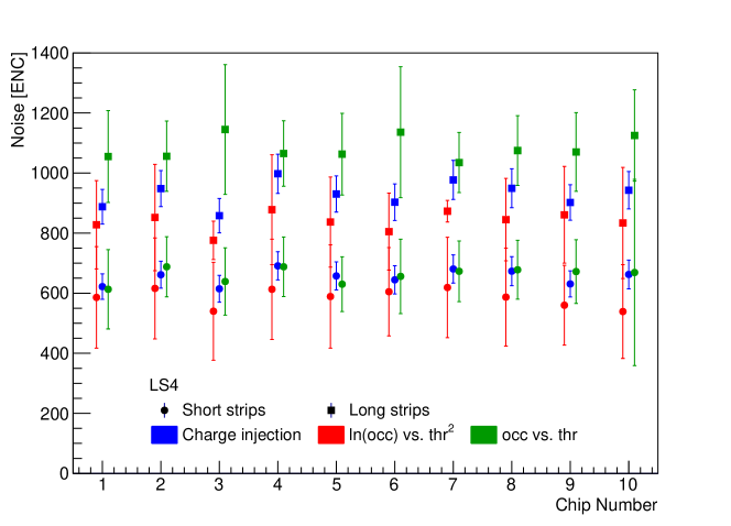
4.5 Sensor hysteresis
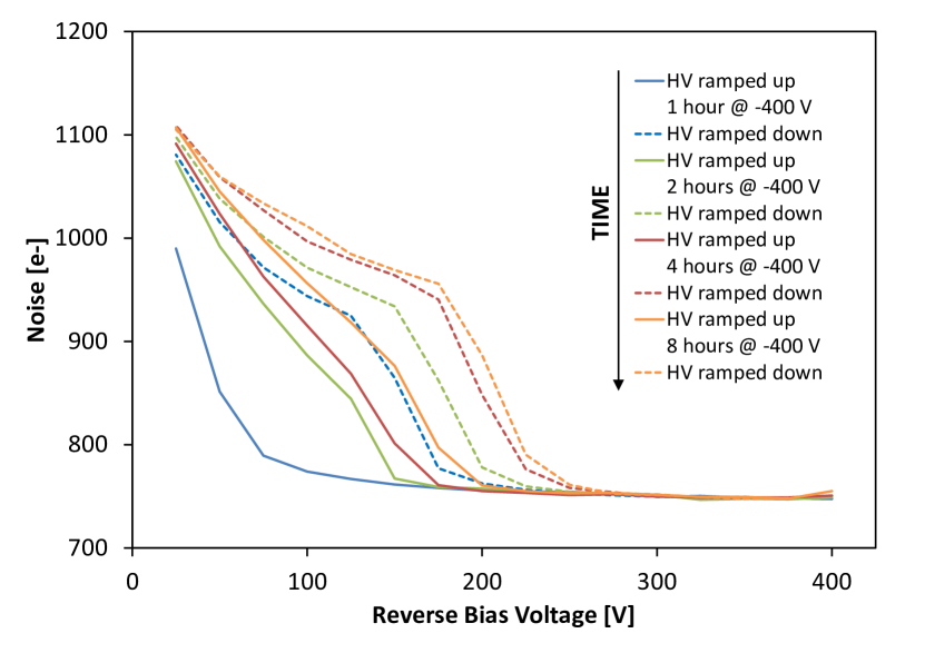
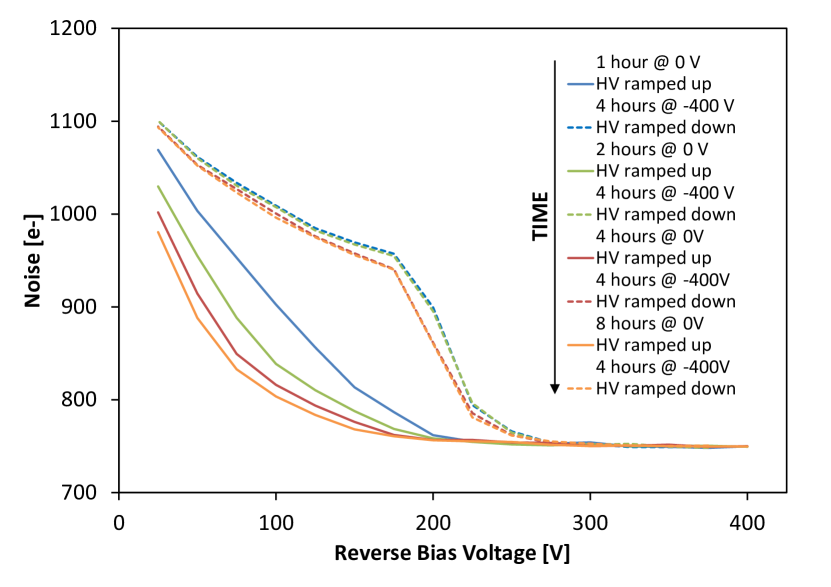
Figure 54 shows the result of running internal charge injection tests when changing the reverse bias voltage of a short strip module. The applied reverse bias voltage was changed in 25 V steps from -25 to -400 V, where the full depletion voltage for this sensor is -370 V. The bias ramp speed was 2 V/s and tests were run immediately after the bias voltage was reached. In the first test, the bias voltage was ramped down immediately after ramping up. The time the sensor was held at -400 V was changed from one to eight hours. As can be seen from the plots, the shapes of both the upward and downward ramp change depended on the biasing history of the sensor. In the second test, the bias voltage was held at -400 V for four hours, and the length of time it was kept unbiased was varied from zero to eight hours. As can be seen, the shape of the downward ramp is independent but the upward ramp shape strongly depends on the time the sensor was left unbiased. Note that prior to the first test, the sensor had been unbiased for more than 24 hours.
These variations are attributed to the increase in inter-strip capacitance (C), which dominates the preamplifier input noise, for reverse bias voltages below the set bias voltage. The effect is described in detail in [31], and is probably caused by localised charge build-up in the surface layers of the sensor. Prolonged biasing of the sensor exacerbates the effect, and hence when ramping down, the noise levels increase compared to those measured when ramping up the bias voltage.
4.6 EMI pick up studies
The effect of induced noise from electromagnetic fields generated by the powerboard components was studied in more detail. In a first investigation, the module susceptibility to an EMI agressor was tested as a function of both distance and frequency. The module was powered by a powerboard glued onto the sensor surface in its nominal position between the two hybrids. Noise was intentionally induced using an external coil of the same type and dimension as the one used on powerboards. The coil was placed with its flux aimed perpendicular to the directions of the signal wire bonds of one of the ABC130 chips, as shown in Figure 55. A frequency generator provided the input with an input power of -15 dBm.
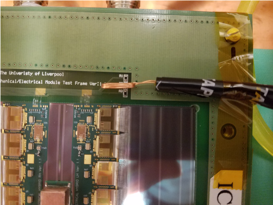
In the first configuration, the coil was placed 1 cm from the sides of the ABC130 wire bonds, and the frequency was scanned between 5 and 50 MHz. A three point gain test was run for each frequency step, and the mean chip noise was calculated for the exposed chip. In addition, prior to turning on the frequency generator, a three-point gain test was run to establish a baseline noise. The induced noise from the coil was assumed to be uncorrelated from existing noise sources without the coil, and therefore the noise from the coil was calculated by subtracting in quadrature with the baseline noise values:
| (1) |
where the sign is positive in cases where the baseline noise was less than the induced noise from the coil and negative otherwise; the latter being possible in cases where very little noise was induced into the module, and due to statistical fluctuations the noise measured with the coil was less than the baseline.
As shown in figure 56, the increase in noise is most pronounced for frequencies in the range of 10 to 25 MHz, and has a strong dependence on proximity to the module. Noise values are shown separately for even and odd channels, corresponding to inner and outer signal bonds. For distances beyond 50 mm, the induced noise from the coil falls to zero. The general shape of the frequency dependence reflects the ABC130 front-end amplifier bandpass. The top wirebond rows have higher pickup than the bottom ones, indicating either an incomplete screening effect, or dependence on the wirebond loop area.
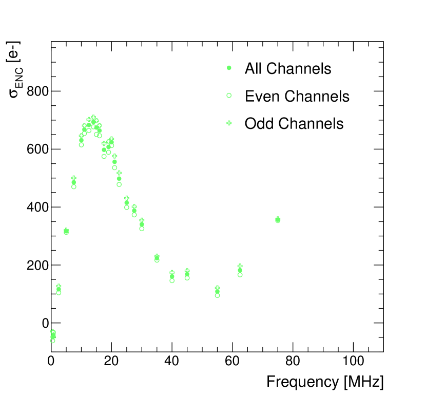
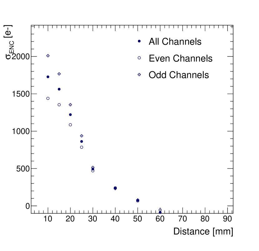
The EMI spectrum from the powerboard was measured with an open loop probe and a network analyzer, both for the board with and without the shieldbox (figure 57(a)). The primary emission spectrum has peaks descending with frequency, which are harmonics of the 2 MHz driving frequency. The shield box provides an attenuation that grows with frequency, consistent with the skin effect properties. The attenuation is direction-dependent. It is about 60 dB upwards and downwards of the powerboards, and about 25 dB on the side. Although the 2 MHz emission is significant, there is a strong reduction of the emission at the peak of the amplifier’s acceptance. The general features of the spectrum have been simulated in SPICE using a model with a buck converter, as shown in figure 57(b), where the measured EMI noise on a module is super-imposed above the simulated power spectrum of the coil.
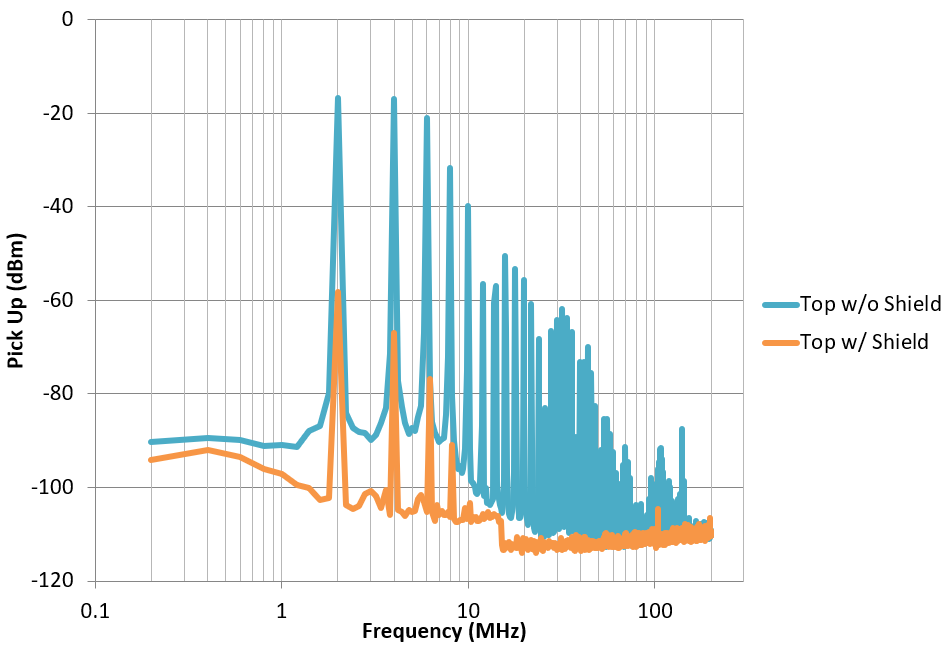
The measurements confirm the existence of many EMI emission harmonics in the front-end amplifier’s bandpass, which can contribute to the readout noise. The strong attenuation provided by the shield box is essential for the unusual placement of the DC-DC converter directly on the module in close proximity to both sensor strips and the front-end circuitry.
4.7 Effect of powerboard on module noise
During the ABC130 barrel module program, each module was tested twice: once after hybrids were mounted, by powering hybrids directly, and again after its powerboard had been mounted, by powering hybrids through the powerboard as intended in the detector. While the additional test was performed to attribute causes of electrical failures during testing to either powerboard or hybrids, the repeated measurements allowed for a comparison of the module performance before and after its powerboard was mounted. Figure 58 shows the ratio of noise measured before and after powerboard attachment for each sensor strip on all of the four strip segments.
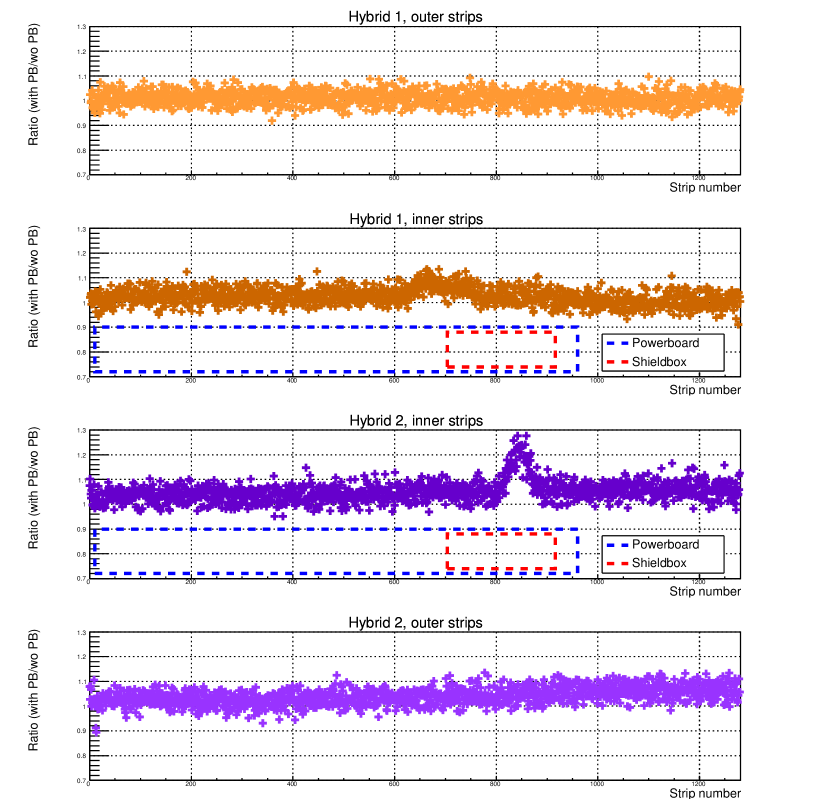
A similar pattern was found for most of the produced barrel modules: while the outer sensor segments, which are not covered by the powerboard, showed mostly flat noise distributions, inner module segments, which are partially covered by the powerboard, consistently showed an increase in the vicinity of the shield box.
In order to compare the noise increase after powerboard attachment, module test results from all produced modules were combined. Since the absolute ratio depends on the environmental conditions during testing, test results from different modules were not combined using the absolute calculated noise ratios. Instead, an average noise ratio was determined for each strip segment in each test using a linear fit. The calculated average was used to determine, on a strip-by-strip base, channels where the calculated noise ratio was more than 2.5 % higher than the average ratio for that strip segment. Each channel which exceeded this threshold was added to a map, which was then compared to the position of the powerboard on the modules (see figure 59).
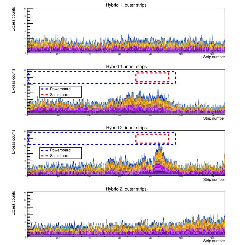
The combination of test results from different modules and construction sites confirmed that the observed noise increase was a systematic effect caused by the presence of the powerboard.
Based on these measurements, the powerboard design was modified to increase its shielding properties.
4.8 Irradiated modules
In order to investigate the radiation tolerance of the ABC130 barrel module, a mixed strip length module was irradiated with protons at the CERN PS to a fluence of , corresponding to the maximum NIEL fluence expected at the end of life-time in the short strip region of the ITk strip barrel. The same charge injection based measurements were performed on this module and the results can be seen in figure 60, which shows the noise and gain of the module before and after irradiation. Only 5 chips are shown due to issues during the assembly process.
As can be seen, there is an increase in the measured noise on the module by about . It is specified that at end of life the detector must have a charged particle detection efficiency of at least and an occupancy from noise hits of no more than . This requirement approximately equates to a requirement of a signal-to-noise ratio (SNR) of at least 10 throughout the life of the experiment. Given the conservative estimate of the charge collection at end of life of () and the measured noise of for the short strips on this module, an SNR of 10.5 is achieved and the end of life requirement is met. The end-of-life requirement has been further studied in test-beam studies [30].
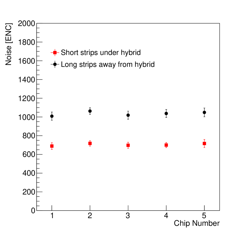
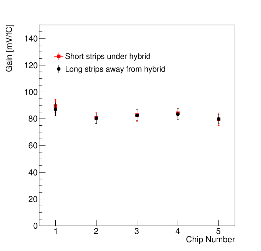
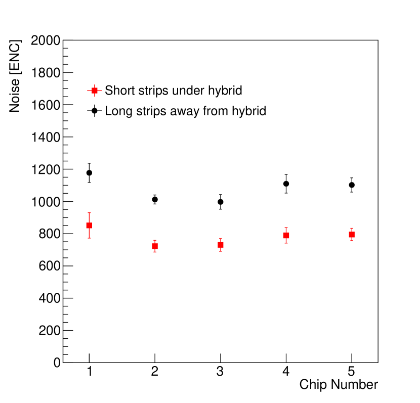
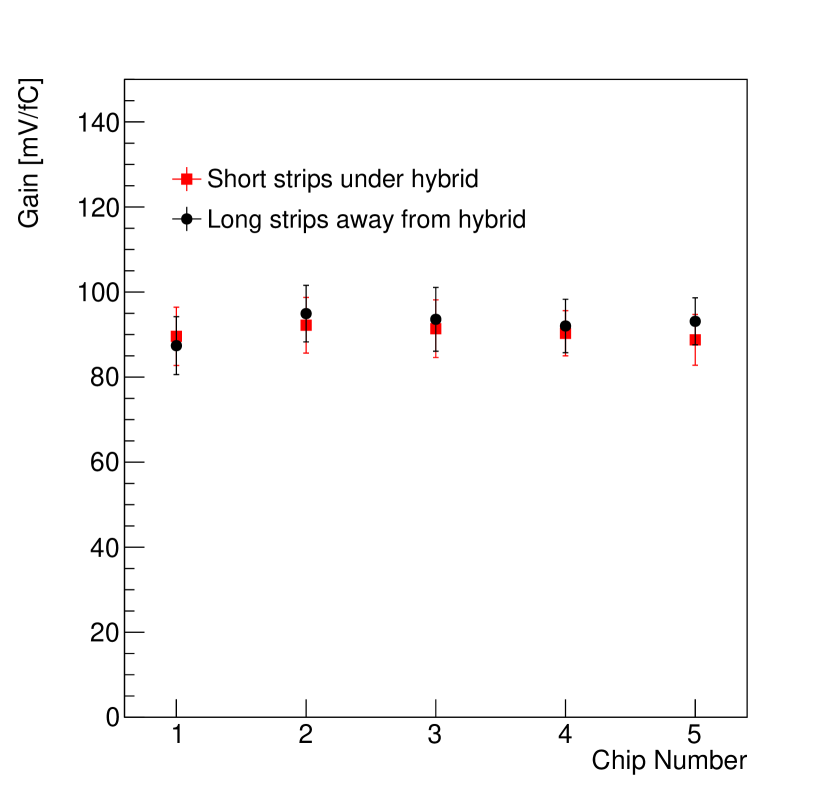
4.9 Bad channel identification
As described in section 3.2.6, the Three Point Gain test can be used to determine electrical characteristics of module channels and assess their quality. This section investigates different types of channel defects and optimising their identification.
4.9.1 Electrical Shorts
Due to a lack of natural abundance of strip defects in the prototype sensors (see figure 36), defects were intentionally added to a short-strip module in the form of additional wire bonds for some of the strips. Three types of defects were added corresponding to different scenarios that could arise:
-
•
bonds from strip to DC pad (added to three strips) to simulate shorts between the strip and implant (pinholes)
-
•
bonds between neighbouring strips (added to four pairs of strips) to simulate shorts at the sensor
-
•
bonds between non-neighbouring strips (added to four pairs of strips) to simulate shorts between ABC130 input channels or signal wirebonds
Figure 61 shows an example of each type of defect.
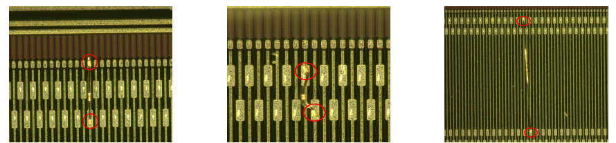
The Three Point Gain test was run after these defects were added. The three strips bonded to simulate pinholes all had normal behaviour. All four pairs bonded to simulate shorts to neighbour strips showed similar behaviour where one channel has high gain and the other has low/nearly zero gain. The threshold scans in figure 62 show an example of this behaviour. Three out of the four pairs of channels bonded to simulate shorts between non-neighbouring strips also showed a similar behaviour. The one pair that had different behaviour may have been due to an issue with wire bonding.
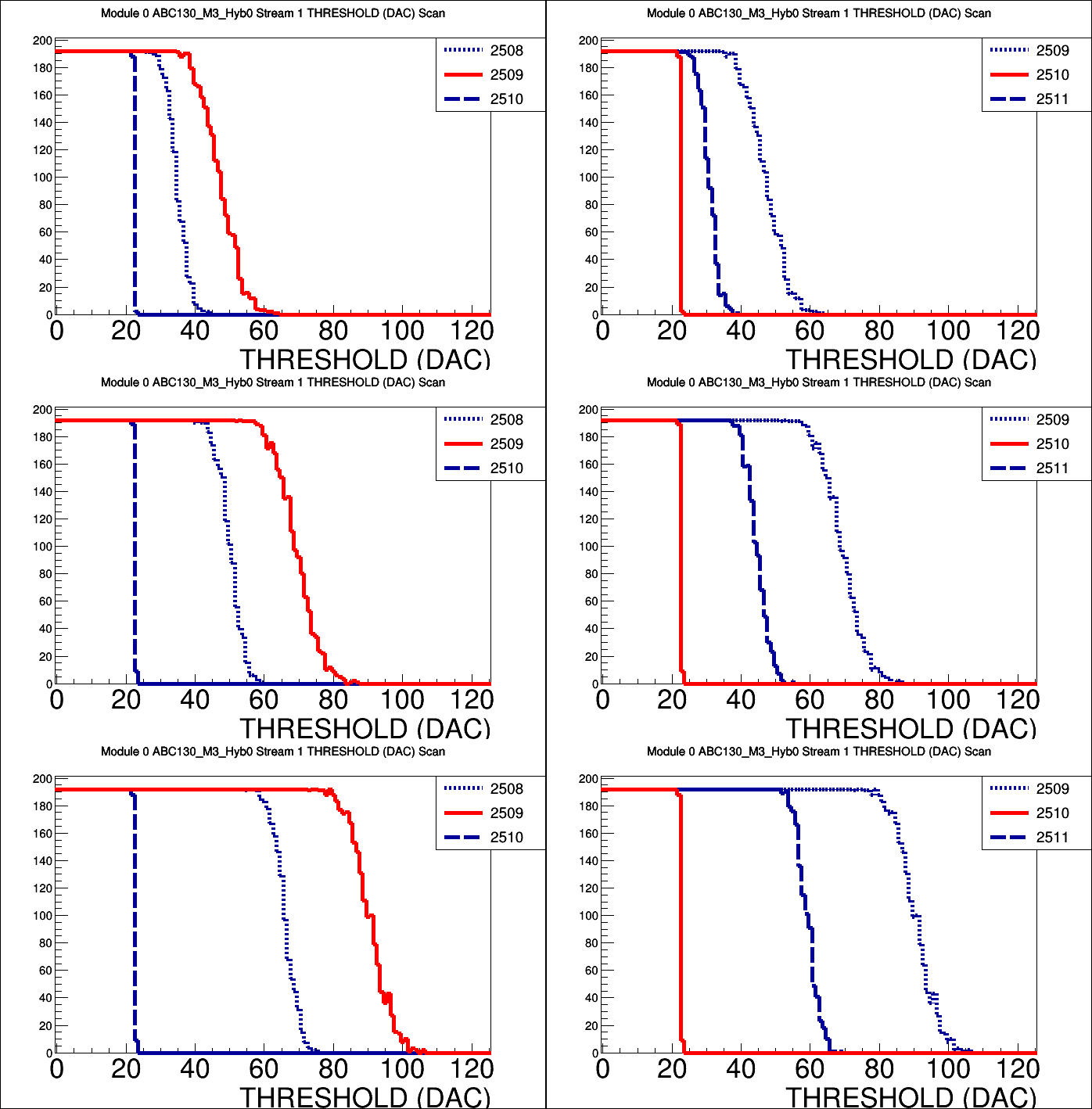
From these results it appears that pinholes cannot be identified from Three Point Gain tests while the shorts between strips can be identified from an obvious pattern. In regards to the inability to identify pinholes, it may be possible that after irradiation they may be visible from these tests and thus will require further investigation.
4.9.2 Unbonded Classification and Bias Voltage
The motivation for this study was to investigate the idea of running a Three Point Gain test at reverse bias voltage below full depletion for the purpose of identifying channels for which the signal bonds have become disconnected. Lowering the bias voltage of the sensor should increase the overall noise of the module and thus make it more distinct compared to hybrid-level noise, which helps to identify unbonded channels.
The classification of channels based on noise measurements is anticipated to be more ambiguous for future ABCstar modules due to a smaller noise dependence on the input capacitance. For illustration purposes, this effect was studied for an R0 module with an ABC130 chip set (see figure 63), which features one row of strips with short length (1.9 cm) [32].
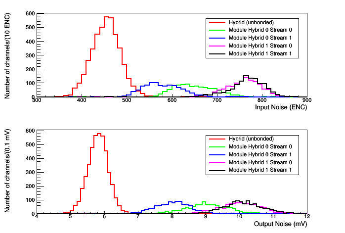
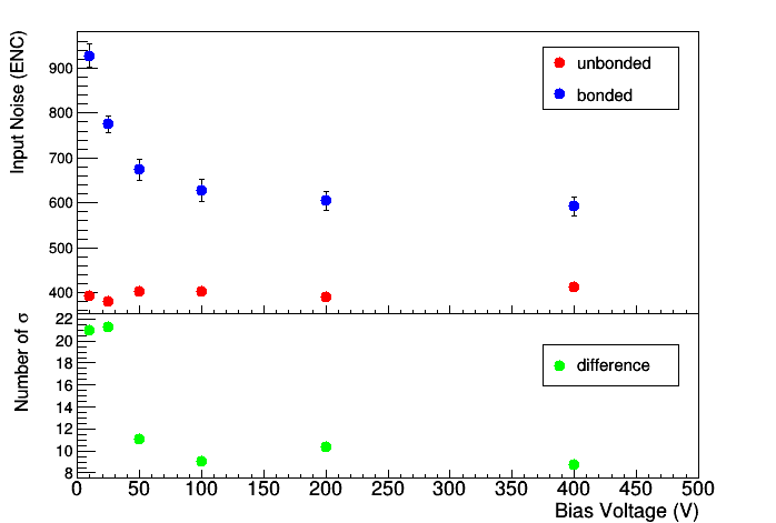
Three Point Gain tests were run at different reverse bias voltages between -1 and -400 V. The tests were conducted using a short-strip module which had a few channels that were intentionally unbonded to use as a comparison. An example of the noise difference between bonded and unbonded channels is shown in figure 64. The optimal value seems to be around -25 V where it is possible to substantially increase the noise while still obtaining reasonable results without large variations in the channel noise that appear at lower bias voltages.
4.10 Current increase with Total Ionising Dose (TID bump)
The 130 nm process used to fabricate the ABC130 chip set is known to be sensitive to certain radiation effects [33]. In particular, NMOS transistors fabricated using this process show an increase in leakage current when exposed to ionizing doses of radiation up to approximately 1 Mrad (full lifetime dose is simulated to be 53.2 Mrad). Continued exposure to ionizing radiation (beyond 1 Mrad) then gradually reduces the leakage current back towards its nominal value. This phenomenon has been named the “TID bump”.
The size of the effect depends both on the characteristics of the transistor and on the characteristics of the radiation. The use of enclosed layout transistors in analog blocks of the chips, such as those which perform the signal amplification and discrimination, completely negates the impact of the TID bump for those transistors. However, the impact is considerable for regions of the chips using digital functionality, where the transistors do not use an enclosed layout. For these portions of the chips, it is crucial to understand the impact of the TID bump, and its dependence on the environmental conditions. Too much leakage current could result in an inability to properly power the chips or to cool the detector.
Chips were tested while being cooled and irradiated at dose rates compatible with those expected during HL-LHC operation. Chips were cooled to between -25 ∘C and 0 ∘C. They were irradiated at dose rates ranging from 0.6 krad/h to 2.5 krad/h; these rates cover the expected range for chips in different positions during nominal HL-LHC operation. The observed increase in leakage currents for these tests ranged between % and %, with smaller increases at higher temperatures and lower dose rates [5] (see figure 65).
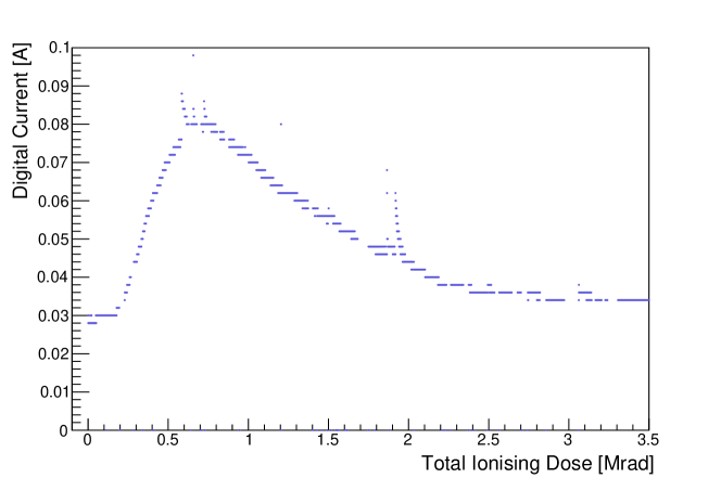
An empirical function was fit to the data in order to describe the dose rate and temperature dependence of the bump for use in thermo-electrical models of the detector.
Furthermore, tests of multiple chips revealed that not only does the size of the bump depend on the environmental conditions, but that there was significant variance in the size of the bump measured across different chips tested in the same conditions. Significant variations in the size of the TID bump were seen both between different chips produced in the same batch, and between chips produced in different batches.
Ultimately, in order to mitigate the current increase, a strategy of pre-irradiation was chosen: chips undergo high dose-rate irradiation up to a dose of Mrad, well beyond the TID bump. Using this method, the chips have already passed the bump so that their leakage current has returned to that before any irradiation. A number of tests performed on annealed chips confirmed that they would not undergo a secondary bump after long room temperature annealing periods between the pre-irradiation and operation at the HL-LHC. These tests include up to 14 months with the chip stored at 80 ∘C and up to 11 months with the chip left powered and running at room temperature. These chips were irradiated to 8 Mrad using Co-60 and re-irradiated at room temperature at 0.7 Mrad/hr using a 3 kV tungsten x-ray tube. The effect of this pre-irradiation procedure can be seen in figure 66.
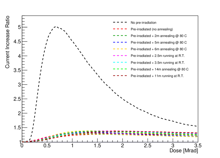
5 Conclusion and Outlook
Within the scope of the ABC130 barrel module programme, about 100 modules were constructed at ten institutes foreseen to assemble barrel modules for the future ITk strip tracker. While a small number of LS modules was built, the majority of assembled modules were SS modules, as their more complicated assembly and readout was considered more challenging. Their construction allowed to develop assembly tools and test procedures for future module construction.
The barrel module prototyping programme demonstrated that the established procedures for assembly and quality control ensured the production of modules within the required specifications. The assembly procedures and developed tooling were found to result in the required module geometries as evidenced by the outcome of metrological surveys. The electrical testing procedures confirmed that the Signal-to-Noise-ratio required by the ATLAS strip tracker for the subsequent module generation could be achieved. Areas for improvement, such as an increased noise under the powerboard shield box, could be identified and corrected in subsequent iterations.
The assembled modules were used to construct complete prototype versions of higher-level detector structures called staves. Staves consist of a carbon fibre core with integrated cooling, power, and data I/O infrastructures on both sides, onto which 13 or 14 modules per side are glued and electrically connected [3]. The availability of 100 barrel modules allowed the assembly of one fully loaded stave, three half loaded staves (where only one side of the stave was fully populated) and one partially loaded double-sided stave (where both stave sides were partially populated with modules). The availability of several populated stave sides permitted tests of fully assembled structures as well as system tests, where potential interactions of neighbour staves could be studied. The extensive test program performed on staves [34] goes beyond the scope of this publication.
The scale and results of this prototyping program demonstrated a high degree of development for all involved components, as well as the module assembly and testing processes. The major driver for the next design evolution was an increase of the trigger rate requirement to MHz range. To address this challenge, a new readout architecture was necessary, instigating the development of the subsequent generation of readout chips called star chips. While ABC130 chips were read out in chains of five chips in series, the star chip set was developed to allow the direct readout of each individual ASIC to increase the bandwidth. A new generation of components based on the star chip design was designed based on the findings from the ABC130 barrel module programme and will be developed into modules for the ITk strip tracker.
Acknowledgements
Individual authors were supported in part by the U.S. Department of Energy under Contract No. DE-AC02-05CH11231. This study was supported by National Key Programme for S&T Research and Development (Grant No.: 2016YFA0400101). The work at SCIPP was supported by the Department of Energy, grant DE-SC0010107. This work was supported by the Science and Technology Facilities Council [grant number ST/R002592/1], the Polish Ministry of Science and Higher Education, Grant No.: DIR/WK/2018/04, the Canada Foundation for Innovation and the Natural Sciences and Engineering Research Council of Canada and the Australian Research Council.
References
- [1] ATLAS Collaboration. The ATLAS Experiment at the CERN Large Hadron Collider. Journal of Instrumentation, 3(08):S08003, 2008.
- [2] S. Kuehn et al. Prototyping of hybrids and modules for the forward silicon strip tracking detector for the ATLAS Phase-II upgrade. Journal of Instrumentation, 12(05):P05015–P05015, 5 2017.
- [3] Sergio Díez et al. A double-sided, shield-less stave prototype for the ATLAS Upgrade strip tracker for the High Luminosity LHC. 9(03):P03012–P03012, mar 2014.
- [4] ATLAS Collaboration. Technical Design Report for the ATLAS Inner Tracker Pixel Detector. Technical Report CERN-LHCC-2017-021. ATLAS-TDR-030, CERN, Geneva, Sep 2017.
- [5] ATLAS Collaboration. Technical Design Report for the ATLAS Inner Tracker Strip Detector. Technical Report CERN-LHCC-2017-005. ATLAS-TDR-025, CERN, Geneva, Apr 2017.
- [6] Y. Unno et al. Development of n+-in-p large-area silicon microstrip sensors for very high radiation environments - ATLAS12 design and initial results. Nucl. Instrum. Meth., A765:80–90, 2014.
- [7] Y. Unno et al. Development of n-on-p silicon sensors for very high radiation environments. Nucl. Instrum. Meth., A636:S24–S30, 2011.
- [8] L. Poley et al. Mapping the depleted area of silicon diodes using a micro-focused X-ray beam. Journal of Instrumentation, 14(03):P03024–P03024, mar 2019.
- [9] L.B.A. Hommels et al. Detailed studies of full-size ATLAS12 sensors. Nuclear Instruments and Methods in Physics Research Section A: Accelerators, Spectrometers, Detectors and Associated Equipment, 831:167 – 173, 2016. Proceedings of the 10th International ”Hiroshima” Symposium on the Development and Application of Semiconductor Tracking Detectors.
- [10] K. Hara and N. Hamasaki and Y. Takahashi and S. Mitsui and Y. Ikegami and Y. Takubo and S. Terada and Y. Unno. Design of Punch-Through Protection of Silicon Microstrip Detector against Accelerator Beam Splash. Physics Procedia, 37:838 – 843, 2012. Proceedings of the 2nd International Conference on Technology and Instrumentation in Particle Physics (TIPP 2011).
- [11] J. Fernández-Tejero et al. Humidity sensitivity of large area silicon sensors: Study and implications. to be published in Nuclear Instruments and Methods in Physics Research Section A: Accelerators, Spectrometers, Detectors and Associated Equipment.
- [12] Y. Unno et al. ATLAS17LS - a large-format prototype silicon strip sensor for long-strip barrel section of ATLAS ITk strip detector. Nucl. Instrum. Meth., TBC:TBC, 2020.
- [13] Francis Anghinolfi et al. ABC130 ASIC Specification v4.6. July 2013. https://documents.epfl.ch/users/n/nl/nlehmann/www/SelfSeededTrigger _MasterThesis/References/ATLASgroup_ABC130Specification_v4-6.pdf.
- [14] W. Dabrowski et al. Design and performance of the ABCD chip for the binary readout of silicon strip detectors in the ATLAS semiconductor tracker. IEEE Transactions on Nuclear Science, 47(6):1843–1850, Dec 2000.
- [15] W. Dabrowski et al. Design and performance of the ABCN-25 readout chip for ATLAS Inner Detector Upgrade. 2009 IEEE Nuclear Science Symposium Conference Record (NSS/MIC), pages 373–380, 2009.
- [16] Scalable Low-Voltage Signaling for 400 mV (SLVS-400). (JESD8-13), October 2001. https://www.jedec.org/standards-documents/docs/jesd-8-13.
- [17] J. Kaplon and M. Noy. Front-end Electronics for SLHC Semiconductor Trackers in CMOS 90 nm and 130 nm Processes. IEEE Transactions on Nuclear Science, 59(4):1611–1620, Aug 2012.
- [18] Francis Anghinolfi et al. Specifications of the ABCStar ASIC v7.66. January 2018. ATLAS internal document: https://edms.cern.ch/ui/file/1809573/1/ABCStar_Spec_07.66.pdf.
- [19] Standard Description of 1.2V CMOS Logic Devices (Normal Range Operations). (JESD76-2), June 2001. https://www.jedec.org/standards-documents/docs/jesd-76-2.
- [20] Standard Test Access Port and Boundary-Scan Architecture. (IEEE Standard 1149.1-2013), May 2013.
- [21] F. Anghinolfi et al. ASIC wafer test system for the ATLAS Semiconductor Tracker front-end chip. IEEE Transactions on Nuclear Science, 49(3):1080–1085, 2002.
- [22] P Leitao, S Feger, et al. Test bench development for the radiation hard GBTX ASIC. Journal of Instrumentation, 10(01):C01038–C01038, Jan 2015.
- [23] S Michelis, B Allongue, G Blanchot, F Faccio, C Fuentes, S Orlandi, S Saggini, S Cengarle, and F Ongaro. DC-DC converters in 0.35m CMOS technology. Journal of Instrumentation, 7(01):C01072–C01072, Jan 2012.
- [24] C. Helling et al. Study of n-on-p sensors breakdown in presence of dielectrics placed on top surface. Nuclear Instruments and Methods in Physics Research Section A: Accelerators, Spectrometers, Detectors and Associated Equipment, 924:147 – 152, 2019. 11th International Hiroshima Symposium on Development and Application of Semiconductor Tracking Detectors.
- [25] L. Poley et al. Alternative glues for the production of ATLAS silicon strip modules for the Phase-II upgrade of the ATLAS Inner Detector. Journal of Instrumentation, 11(05):P05017–P05017, May 2016.
- [26] Edison Opto Corporation. Federal 3535 UV & IR Series Datasheet, 4 edition. https://www.edison-opto.com.tw/wp-content/uploads/2019/09/Edison-Opto-datasheet-Federal-3535-UV-IR-Series_SAPv9.pdf.
- [27] Digilent Inc. Atlys FPGA development board documention. https://reference.digilentinc.com/reference/programmable-logic/atlys/start.
- [28] Digilent Inc. Nexys Video FPGA development board documention. https://reference.digilentinc.com/reference/programmable-logic/atlys/start.
- [29] I. Antcheva et al. ROOT — A C++ framework for petabyte data storage, statistical analysis and visualization. Computer Physics Communications, 182(6):1384 – 1385, 2011.
- [30] A.J. Blue et al. Test beam evaluation of silicon strip modules for ATLAS phase-II strip tracker upgrade. Nuclear Instruments and Methods in Physics Research Section A: Accelerators, Spectrometers, Detectors and Associated Equipment, 924:108 – 111, 2019. 11th International Hiroshima Symposium on Development and Application of Semiconductor Tracking Detectors.
- [31] C. T. Klein. Investigation of performance and the influence of environmental conditions on strip detectors for the ATLAS Inner Tracker Upgrade. PhD thesis, Cavendish Laboratory, Cambridge, 2019.
- [32] C. Lacasta et al. Design of the first full size ATLAS ITk strip sensor for the endcap region. Nucl. Instrum. Meth. A, 924:137–141, 2019.
- [33] F Faccio and G Cervelli. Radiation-induced edge effects in deep submicron CMOS transistors. IEEE Trans. Nucl. Sci., 52:2413–2420, 2005.
- [34] Peter W. Phillips. Design, Development, Characterisation and Operation of ATLAS ITk Strip Staves. DPhil Thesis submitted to the University of Oxford, 2020.