Global strain-induced scalar potential in graphene devices
Abstract
By mechanically distorting a crystal lattice it is possible to engineer the electronic and optical properties of a material. In graphene, one of the major effects of such a distortion is an energy shift of the Dirac point, often described as a scalar potential. We demonstrate how such a scalar potential can be generated systematically over an entire electronic device and how the resulting changes in the graphene work function can be detected in transport experiments. Combined with Raman spectroscopy, we obtain a characteristic scalar potential consistent with recent theoretical estimates. This direct evidence for a scalar potential on a macroscopic scale due to deterministically generated strain in graphene paves the way for engineering the optical and electronic properties of graphene and similar materials by using external strain.
Graphene is a model system on which a large variety of new and prominent physical phenomena have been discovered Castro Neto et al. (2009); Das Sarma et al. (2011); Goerbig (2011); Yankowitz et al. (2019). A particularly promising topic is the control of its electronic properties by external strain, which has been extensively studied theoretically. The predicted strain effects in the low-energy band structure of graphene can be summarized as changes in the magnitude and isotropy of the Fermi velocity and thus in the density of states (DoS) Pereira et al. (2009); Choi et al. (2010); de Juan et al. (2012); Grassano et al. (2020), shifts in the energy of the Dirac point, which is typically incorporated as a scalar potential Guinea et al. (2010); Choi et al. (2010); Grassano et al. (2020), and changes in the position of the Dirac cone in the two-dimensional Brillouin zone, often described by a pseudo-vector potential acting on the valley degree of freedom Fogler et al. (2008); Guinea et al. (2009, 2010); Low and Guinea (2010); Uchoa and Barlas (2013); Zhu et al. (2015). Previous experiments explored some of these strain effects on a local scale using scanning tunneling microscopy Levy et al. (2010); Klimov et al. (2012); Yan et al. (2012); Guo et al. (2012); Lu et al. (2012); Jiang et al. (2017); Liu et al. (2018); Jia et al. (2019); Li et al. (2020), Kelvin probe force microscopy He et al. (2015); Volodin et al. (2017), or angle-resolved photoemission spectroscopy Nigge et al. (2019). However, studying strain effects in transport measurements and on a global scale is still challenging due to the lack of in situ strain tunability Shioya et al. (2015); Wu et al. (2018); Liu et al. (2018) or ambiguities resulting from simultaneous changes in the gate capacitance Huang et al. (2011); Guan and Du (2017); Wang et al. (2019a).
Here, we demonstrate the formation of a scalar potential generated by systematically tuning the strain in a micrometer sized graphene electronic device and investigate its effects on two fundamental electron transport phenomena, quasi-ballistic transport and the quantum Hall effect (QHE). We find that all investigated transport characteristics are shifted systematically in gate voltage, qualitatively and quantitatively consistent with the expectations for the scalar potential generated by the applied strain, where the strain values are confirmed by separate Raman spectroscopy experiments.
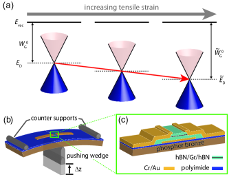
The work function (WF) of a material, i.e. the energy required to remove an electron from the material, is defined as the difference between the vacuum level and the Fermi level of the material Cahen and Kahn (2003). For undoped graphene, coincides with the Dirac point energy Castro Neto et al. (2009), therefore the WF of undoped graphene is . A strain-induced scalar potential shifts , which therefore leads to a change in . With increasing tensile strain, the scalar potential shifts to lower values, resulting in an increase in Choi et al. (2010); Grassano et al. (2020), as illustrated in Fig. 1(a). Quantitatively, strain shifts to , where is the scalar potential, and can be written as Choi et al. (2010); Guinea et al. (2010); Grassano et al. (2020):
| (1) |
with and the diagonal components of the strain tensor, and a constant defined for small strain values. The value of is not well established and theoretical values are reported in the range between and Choi et al. (2010); Guinea et al. (2010); Grassano et al. (2020).
How we generate strain in our experiments in an on-chip fully encapsulated graphene device is illustrated in Fig. 1(b): in a three-point bending setup a flexible substrate with the devices fabricated in the center is bent by pushing a central wedge against two fixed counter supports by a displacement of Wang et al. (2019a). The schematics of the device configuration is shown in Fig. 1(c). The edge contacts to graphene act as clamps for the strain generation and at the same time as electrical contacts for transport experiments Wang et al. (2019a). A metallic global bottom gate is used to tune the charge carrier density in the device. The on-chip hBN encapsulation ensures that the geometrical capacitance between the gate and the graphene is not changed in the straining process. Here, we investigate strain effects on devices with a rectangular geometry, which results in an essentially homogeneous uniaxial strain field. Details of the device fabrication and the strain field pattern are discussed in Wang et al. (2019a).
In our devices, the grounded graphene sheet and the metallic gate essentially form a plate capacitor. The detailed diagram of energy level alignment and its modification by strain are given in the Supplemental Material. The strain-induced scalar potential shifts the Dirac point, resulting in a systematic change in the charge carrier density of the device at a given gate voltage, which we detect in transport experiments.
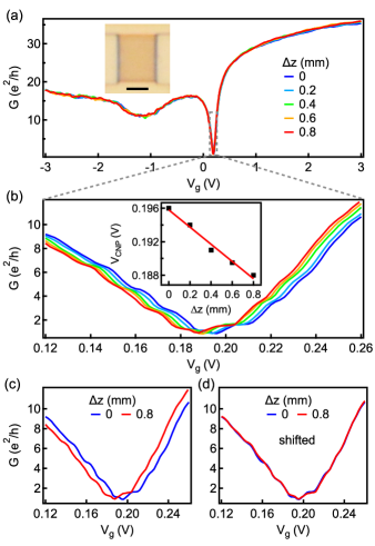
To investigate the strain effect, we perform transport experiments at liquid helium temperature () using standard low-frequency lock-in techniques. The two-terminal differential conductance of a square device is measured as a function of for different bendings of the substrate. An overview measurement is plotted in Fig. 2(a), on the scale of which no significant strain effects can be observed. The charge neutrality point (CNP) occurs at a positive gate voltage. From a linear fit near the CNP we find a field effect charge carrier mobility of , independent of , suggesting a high device quality and that random strain fluctuations are probably not dominating scattering processes here Wang et al. (2020). The additional conductance minimum at may originate from a large contact doping due to the overlap of the electrodes with the graphene region near the edge contacts Du et al. (2018), or from a super-superlattice effect in encapsulated graphene when both the top and the bottom hBN layers are aligned to the graphene lattice Wang et al. (2019b).
The zoom-in to the CNP plotted in Fig. 2(b) shows very regular oscillations in conductance, which we tentatively attribute to Fabry-Pérot resonances in the regions near the electrical contacts with a different doping compared to the graphene bulk Young and Kim (2009); Rickhaus et al. (2013); Grushina et al. (2013); Handschin et al. (2017) (see Supplemental Material for a detailed discussion). With increasing and therefore increasing tensile strain, these conductance oscillations are shifted systematically to lower gate voltages. This effect is fully reversible with deceasing , which is demonstrated in the Supplemental Material. The strain-induced shift is best seen by following the CNP: in the inset of Fig. 2(b) we plot the gate voltage of minimum conductance, as a function of , which shows a linear decrease with increasing , consistent with the picture described in the Supplemental Material. To demonstrate that the complete conductance curves are shifted with strain, we plot in Fig. 2(c) the two curves with the lowest () and the highest () strain values, and in Fig. 2(d) the same data, but with the curve (red) shifted by in . We find that all conductance curves merge to the same curve as at (blue) when shifted by a constant gate voltage offset. This shift we attribute to a strain-induced scalar potential in the graphene sheet. We note that this effect is very different from bending-induced changes in the gate capacitance found in suspended samples, where the axis is rescaled by a constant factor Wang et al. (2019a).
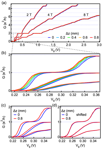
To demonstrate that this is a general effect, independent of the device or the physical origin of the transport characteristics, we have investigated more than 5 devices, all showing similar effects (another example is provided in the Supplemental Material). Here, we now focus on the impact of homogeneous uniaxial strain on the QHE in the same device, and perform a similar analysis as for the zero field measurements. Figure 3(a) shows the two-terminal differential conductance as a function of the gate voltage for three different quantizing magnetic fields, , and for different values. Typical quantum Hall plateaus of graphene can be observed on the electron side, with small deviations of the plateau conductances from the quantized values 2, 6, 10 due to the contact resistance. The plateaus at the filling factors and are well developed alreday at , and more broken symmetry states and fractional quantum Hall states can be observed at Bolotin et al. (2009); Du et al. (2009); Dean et al. (2011), again highlighting the very good device quality. In contrast, the plateaus on the hole side are not well developed (see Supplemental Material) presumably due to a p-n junction forming near the contacts Özyilmaz et al. (2007); Amet et al. (2014). Comparing the measurements for different on this scale shows no clear strain effects. However, in the data near the CNP shown in Fig. 3(b), we again find a systematic shift in with increasing . The clear offset between the curve (red) and the curve (blue) is shown in Fig. 3(c). Shifting the red curve by , as shown in Fig. 3(d), the two curves are virtually identical, in the same manner and with the same shift as discussed for Fig. 2 with the device at zero magnetic field. Since the QHE is quite a different transport regime than quasi-ballistic transport, the observed effect is very general and we attribute it to a strain-induced scalar potential.
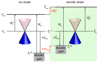
We now extract the scalar potential from the transport experiments by evaluating the shift between the minimum () and maximum strain (). We assume that a specific conductance feature, for example the CNP, or a QHE transition, occurs at a characteristic carrier density. Here we use the CNP as an example for extracting the scalar potential. Figure 4 shows the energy level alignment of the graphene gated to the CNP for the cases with and without strain. Different gate voltages are needed to gate the graphene to the CNP due to the strain-induced changes in the Dirac point energy (see Supplemental Material for details). At the CNP, the strain-induced scalar potential at can be directly extracted from Fig. 4 and the inset of Fig. 2(b) as:
| (2) |
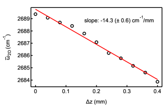
To determine in Eq. 1, we need to estimate the applied strain. This we achieve using spatially resolved Raman spectroscopy at room temperature on the same device Mohiuddin et al. (2009); Huang et al. (2010); Wang et al. (2019a). For small uniaxial strain, a single Lorentzian describes the graphene Raman 2D peak, with the center frequency redshifting linearly with increasing tensile strain. Figure 5 shows the mean center frequency averaged over the entire device area as a function of . With increasing , shifts to lower values, indicating an increasing average strain in the graphene Wang et al. (2019a). Since the displacement is much smaller than the length of the substrate, the strain increases linearly with , with a slope of extracted by linear fitting. Using from the literature Mohr et al. (2009), we obtain a value for the induced tensile strain of at . With this calibration of the strain value, we now deduce the characteristic scalar potential constant , which is within the range predicted by theory Choi et al. (2010); Guinea et al. (2010); Grassano et al. (2020) and is consistent with the most recent calculations Grassano et al. (2020).
In conclusion, we have demonstrated how large scale homogeneous strain in a graphene electronic device results in a scalar potential, which we detect using transport experiments in two different regimes. Combined with strain values extracted from Raman spectroscopy on the same device, we report the first systematically measured characteristic number for the scalar potential strength, consistent with the most recent theoretical calculations. This in situ strain tuning and the combination of transport and Raman measurements thus confirms the scalar potential as the origin of the observed strain effects. Our study forms the basis to investigate strain effects in transport experiments, which is crucial for future strain engineering in graphene and related 2D materials, such as generating a strain-induced in-plane electric field for observing the phenomenon of the Landau level collapse Grassano et al. (2020), realizing graphene quantum strain transistors McRae et al. (2019), or creating a pseudo-magnetic field with a non-uniform strain field Guinea et al. (2009, 2010).
.1 Author contributions
L.W. fabricated the devices, performed the measurements and did the data analysis. A.B., P.M., S.Z. and C.S. helped to understand the data. B.V. performed parts of the Raman measurements. D.I. supported the sample fabrication. K.W. and T.T. provided the high-quality hBN. C.S. initiated and supervised the project. L.W. and A.B. wrote the paper and all authors discussed the results and worked on the manuscript. All data in this publication are available in numerical form at: https://doi.org/10.5281/zenodo.4017429.
Acknowledgments
This work has received funding from the Swiss Nanoscience Institute (SNI), the ERC project TopSupra (787414), the European Union Horizon 2020 research and innovation programme under grant agreement No. 785219 (Graphene Flagship), the Swiss National Science Foundation, the Swiss NCCR QSIT, Topograph, FlagERA network and from the OTKA FK-123894 grants. P.M. acknowledges support from the Bolyai Fellowship, the Marie Curie grant, Topograph Flagera network and the National Research, Development and Innovation Fund of Hungary within the Quantum Technology National Excellence Program (Project No. 2017-1.2.1-NKP-2017-00001). K.W. and T.T. acknowledge support from the Elemental Strategy Initiative conducted by the MEXT, Japan, Grant Number JPMXP0112101001, JSPS KAKENHI Grant Numbers JP20H00354 and the CREST(JPMJCR15F3), JST. The authors thank Francisco Guinea, Peter Rickhaus, János Koltai, László Oroszlány, Zoltán Tajkov and András Pályi for fruitful discussions, and Sascha Martin and his team for their technical support.
References
- Castro Neto et al. (2009) A. H. Castro Neto, F. Guinea, N. M. R. Peres, K. S. Novoselov, and A. K. Geim, Rev. Mod. Phys. 81, 109 (2009).
- Das Sarma et al. (2011) S. Das Sarma, S. Adam, E. H. Hwang, and E. Rossi, Rev. Mod. Phys. 83, 407 (2011).
- Goerbig (2011) M. O. Goerbig, Rev. Mod. Phys. 83, 1193 (2011).
- Yankowitz et al. (2019) M. Yankowitz, Q. Ma, P. Jarillo-Herrero, and B. J. LeRoy, Nature Reviews Physics 1, 112 (2019).
- Pereira et al. (2009) V. M. Pereira, A. H. Castro Neto, and N. M. R. Peres, Phys. Rev. B 80, 045401 (2009).
- Choi et al. (2010) S.-M. Choi, S.-H. Jhi, and Y.-W. Son, Phys. Rev. B 81, 081407 (2010).
- de Juan et al. (2012) F. de Juan, M. Sturla, and M. A. H. Vozmediano, Phys. Rev. Lett. 108, 227205 (2012).
- Grassano et al. (2020) D. Grassano, M. D’Alessandro, O. Pulci, S. G. Sharapov, V. P. Gusynin, and A. A. Varlamov, Phys. Rev. B 101, 245115 (2020).
- Guinea et al. (2010) F. Guinea, A. K. Geim, M. I. Katsnelson, and K. S. Novoselov, Phys. Rev. B 81, 035408 (2010).
- Fogler et al. (2008) M. M. Fogler, F. Guinea, and M. I. Katsnelson, Phys. Rev. Lett. 101, 226804 (2008).
- Guinea et al. (2009) F. Guinea, M. I. Katsnelson, and A. K. Geim, Nature Physics 6, 30 (2009).
- Low and Guinea (2010) T. Low and F. Guinea, Nano Lett. 10, 3551 (2010).
- Uchoa and Barlas (2013) B. Uchoa and Y. Barlas, Phys. Rev. Lett. 111, 046604 (2013).
- Zhu et al. (2015) S. Zhu, J. A. Stroscio, and T. Li, Phys. Rev. Lett. 115, 245501 (2015).
- Levy et al. (2010) N. Levy, S. A. Burke, K. L. Meaker, M. Panlasigui, A. Zettl, F. Guinea, A. H. C. Neto, and M. F. Crommie, Science 329, 544 (2010).
- Klimov et al. (2012) N. N. Klimov, S. Jung, S. Zhu, T. Li, C. A. Wright, S. D. Solares, D. B. Newell, N. B. Zhitenev, and J. A. Stroscio, Science 336, 1557 (2012).
- Yan et al. (2012) H. Yan, Y. Sun, L. He, J.-C. Nie, and M. H. W. Chan, Phys. Rev. B 85, 035422 (2012).
- Guo et al. (2012) D. Guo, T. Kondo, T. Machida, K. Iwatake, S. Okada, and J. Nakamura, Nature Communications 3 (2012).
- Lu et al. (2012) J. Lu, A. H. C. Neto, and K. P. Loh, Nature Communications 3, 823 (2012).
- Jiang et al. (2017) Y. Jiang, J. Mao, J. Duan, X. Lai, K. Watanabe, T. Taniguchi, and E. Y. Andrei, Nano Lett. 17, 2839 (2017).
- Liu et al. (2018) Y. Liu, J. N. B. Rodrigues, Y. Z. Luo, L. Li, A. Carvalho, M. Yang, E. Laksono, J. Lu, Y. Bao, H. Xu, S. J. R. Tan, Z. Qiu, C. H. Sow, Y. P. Feng, A. H. C. Neto, S. Adam, J. Lu, and K. P. Loh, Nature Nanotechnology 13, 828 (2018).
- Jia et al. (2019) P. Jia, W. Chen, J. Qiao, M. Zhang, X. Zheng, Z. Xue, R. Liang, C. Tian, L. He, Z. Di, and X. Wang, Nature Communications 10, 3127 (2019).
- Li et al. (2020) S.-Y. Li, Y. Su, Y.-N. Ren, and L. He, Phys. Rev. Lett. 124, 106802 (2020).
- He et al. (2015) X. He, N. Tang, X. Sun, L. Gan, F. Ke, T. Wang, F. Xu, X. Wang, X. Yang, W. Ge, and B. Shen, Applied Physics Letters 106, 043106 (2015).
- Volodin et al. (2017) A. Volodin, C. Van Haesendonck, O. Leenaerts, B. Partoens, and F. M. Peeters, Applied Physics Letters 110, 193101 (2017).
- Nigge et al. (2019) P. Nigge, A. C. Qu, É. Lantagne-Hurtubise, E. Mårsell, S. Link, G. Tom, M. Zonno, M. Michiardi, M. Schneider, S. Zhdanovich, G. Levy, U. Starke, C. Gutiérrez, D. Bonn, S. A. Burke, M. Franz, and A. Damascelli, Science Advances 5 (2019), 10.1126/sciadv.aaw5593.
- Shioya et al. (2015) H. Shioya, S. Russo, M. Yamamoto, M. F. Craciun, and S. Tarucha, Nano Lett. 15, 7943 (2015).
- Wu et al. (2018) Y. Wu, D. Zhai, C. Pan, B. Cheng, T. Taniguchi, K. Watanabe, N. Sandler, and M. Bockrath, Nano Lett. 18, 64 (2018).
- Huang et al. (2011) M. Huang, T. A. Pascal, H. Kim, W. A. Goddard, and J. R. Greer, Nano Lett. 11, 1241 (2011).
- Guan and Du (2017) F. Guan and X. Du, Nano Lett. 17, 7009 (2017).
- Wang et al. (2019a) L. Wang, S. Zihlmann, A. Baumgartner, J. Overbeck, K. Watanabe, T. Taniguchi, P. Makk, and C. Schönenberger, Nano Lett. 19, 4097 (2019a).
- Cahen and Kahn (2003) D. Cahen and A. Kahn, Advanced Materials 15, 271 (2003).
- Wang et al. (2020) L. Wang, P. Makk, S. Zihlmann, A. Baumgartner, D. I. Indolese, K. Watanabe, T. Taniguchi, and C. Schönenberger, Phys. Rev. Lett. 124, 157701 (2020).
- Du et al. (2018) R. Du, M.-H. Liu, J. Mohrmann, F. Wu, R. Krupke, H. von Löhneysen, K. Richter, and R. Danneau, Phys. Rev. Lett. 121, 127706 (2018).
- Wang et al. (2019b) L. Wang, S. Zihlmann, M.-H. Liu, P. Makk, K. Watanabe, T. Taniguchi, A. Baumgartner, and C. Schönenberger, Nano Lett. 19, 2371 (2019b).
- Young and Kim (2009) A. F. Young and P. Kim, Nature Physics 5, 222 (2009).
- Rickhaus et al. (2013) P. Rickhaus, R. Maurand, M.-H. Liu, M. Weiss, K. Richter, and C. Schönenberger, Nature Communications 4 (2013).
- Grushina et al. (2013) A. L. Grushina, D.-K. Ki, and A. F. Morpurgo, Applied Physics Letters 102, 223102 (2013).
- Handschin et al. (2017) C. Handschin, P. Makk, P. Rickhaus, M.-H. Liu, K. Watanabe, T. Taniguchi, K. Richter, and C. Schönenberger, Nano Lett. 17, 328 (2017).
- Bolotin et al. (2009) K. I. Bolotin, F. Ghahari, M. D. Shulman, H. L. Stormer, and P. Kim, Nature 462, 196 (2009).
- Du et al. (2009) X. Du, I. Skachko, F. Duerr, A. Luican, and E. Y. Andrei, Nature 462, 192 (2009).
- Dean et al. (2011) C. R. Dean, A. F. Young, P. Cadden-Zimansky, L. Wang, H. Ren, K. Watanabe, T. Taniguchi, P. Kim, J. Hone, and K. L. Shepard, Nature Physics 7, 693 (2011).
- Özyilmaz et al. (2007) B. Özyilmaz, P. Jarillo-Herrero, D. Efetov, D. A. Abanin, L. S. Levitov, and P. Kim, Phys. Rev. Lett. 99, 166804 (2007).
- Amet et al. (2014) F. Amet, J. R. Williams, K. Watanabe, T. Taniguchi, and D. Goldhaber-Gordon, Phys. Rev. Lett. 112, 196601 (2014).
- Mohiuddin et al. (2009) T. M. G. Mohiuddin, A. Lombardo, R. R. Nair, A. Bonetti, G. Savini, R. Jalil, N. Bonini, D. M. Basko, C. Galiotis, N. Marzari, K. S. Novoselov, A. K. Geim, and A. C. Ferrari, Phys. Rev. B 79, 205433 (2009).
- Huang et al. (2010) M. Huang, H. Yan, T. F. Heinz, and J. Hone, Nano Lett. 10, 4074 (2010).
- Mohr et al. (2009) M. Mohr, K. Papagelis, J. Maultzsch, and C. Thomsen, Phys. Rev. B 80, 205410 (2009).
- McRae et al. (2019) A. McRae, G. Wei, and A. Champagne, Phys. Rev. Applied 11, 054019 (2019).